Separate-Path Electron and Hole Transport
Across -Stacked Ferroelectrics
for Photovoltaic Applications.
Abstract
Abstract: Electron and hole separate-path transport is theoretically found in the -stacked organic layers and columns. This effect might be a solution for the charge recombination problem. The building molecules, named 1,3,5-tricyano-2,4,6-tricarboxy-benzene, contain the mesogenic flat aromatic part and the terminal dipole groups which make the system ferroelectric. The diffusion path of the electrons cuts through the aromatic rings, while holes hop between the dipole groups. The transmission function and the charge mobilities, especially for the holes, are very sensitive to the distance between the molecular rings, due to the overlap of the -type orbitals. We verified that the separation of the diffusion paths is not destroyed by the application of the graphene leads. These features make the system suitable for the efficient solar cells, with the carrier mobilities higher than these in the organometal halide perovskites.
I Introduction
The effect of charge carriers recombination is a very unwanted phenomenon in the photovoltaic materials. There are various attempts to avoid this process in novel solar cell devices. One of the most popular solution, valid for electrons as well as holes, is an addition of the charge trapping layers. These layers selectively permit carriers transport across the multi–junctions. For example, the polymer solar cells equipped with the PEDOT:PSS layers allow to extract hole carriers before they arrive at the anode.pedot:pss Recently, similar hole trapping function has been found for the graphene oxide nanoribbons.GON It has been shown, that the parameters of the metal–oxide–free methylammonium lead iodide perovskite–based solar cells are also improved by the charge transport layers.Olga
On the other hand, the simultaneous trapping of the electrons and holes limits the photovoltaic efficiency. This is an inevitable effect in many systems. The organometal halide perovskites, where the liquid ionscpl1 and surface statesjpcl2 grab both types of carriers are the examples. Another performance key factor is the material structure,natnano1 particularly important in the solution processed organometal trihalide perovskite solar cells. For this kind of systems, planar heterojunctions are less effective than the mesosuperstructured perovskites, regarding the occurrence of the sub gap states, but superior in terms of carrier mobility.acsnano1 ; pccp1 Luckily, the efficiency grows again at very high fluences in the presence of the sub gap states,model1 and the trap-states density can be optimized in terms of the grain size of nanocrystals.science1 In addition, under temperature gradient, several structural phase transitions may occur in these materials, and this fact also influences the diffusion lengths.AFM1
Modern approach to increase the solar cell efficiency goes towards the so–called bulk heterojunctions, where the granular structure of two materials, the donor-type (e.g. polymers) and acceptor-type (e.g. fullerenes), might be regular or graded.bulkhetero It has been found that a larger grade of the composition corresponds to wider charge transportation path and larger effective conductivity.bulkhetero Alternatively to the bulk heterojunctions, the ordered donor-acceptor materials – integrated heterojunctions – have been synthesized.IHJ They are composed of two molecules integrated in the covalent organic frameworks. Recently, these kind of materials gain an attention for their photo-active properties.IHJ ; Bein-3 ; Bein-4 ; Bein-5
An addition of the inter-layer aligns the energy levels of the multijunction device, in such a way that they form a cascade, efficiently reduces the electron-hole recombination.cascade The above effect is intensified if one uses the high/low work-function material for the anode/cathode. This tuning might be done by an adsorption of the dipole moieties.workOH
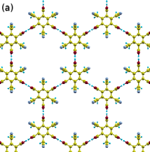
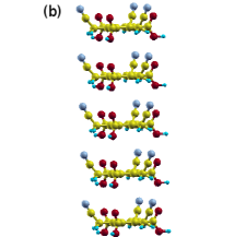
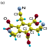
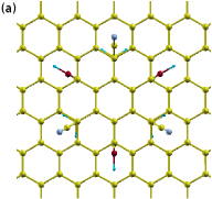
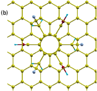
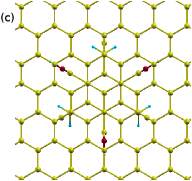
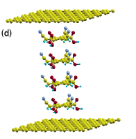
In this work, we present a new solution to the charge-carriers recombination problem – the electron and hole separate-path transport. The considered system has been described in our previous workprevious for its ferroelectric properties. The studied layers are characterized by the cascade energy levels alignment, gradual donor–acceptor layers sequence, and the dipole-proximity tunable work function of the graphene electrodes. In Figs. 1(a)-(c), we present the system which consists of the flat benzene-based molecules, terminated with the cyano groups (NCCH2), that are responsible for the ferroelectric properties, and the carboxy groups (OCOH), that form the hydrogen bonds within the planes. The molecules are named 1,3,5-tricyano-2,4,6-tricarboxy-benzene and their chemical formula reads C6-3(NCCH2)-3(OCOH). The band gap of the 2D layer is around 3.6 eV, while for the columnar stacks is 2.95 eV. We focused on localization of the diffusion paths, but also analyzed the electron and hole mobilities within the planes and across the stacks.
The considered building molecules represent the most simplified model molecules possessing the desired properties. Systems similar to the considered ones, could be realized in industry by modifications of the existing columnar liquid crystals,LC or via the self-assembly of the 2D molecular systems, for example on graphene. This has been reported in the experimentalgraphorder and theoretical works.Lublin Alternatively, one could base on the production processes of the covalent organic frameworksBein-1 ; Berkeley using the external electric field in order to orient all dipole groups ferroelectrically, and avoid formation of the antiferroelectrically coupled domains.Horiuchi
The ferroelectric hydrogen–bonded organic frameworksprevious ; Sobol could be obtained by modifications of the covalent integrated heterojunctionsIHJ or bulk organic ferrolectrics.Horiuchi-2 ; Horiuchi-3 We expect that these frameworks would be interesting for the solar cell community, opening a new door for the efficient photovoltaic devices.
II Method
We calculated various material properties derived from the electronic states obtained within the density functional theory (DFT). All calculations, except for the transmission function, were performed employing the Quantum ESPRESSO suite of codes.qe The density of states (DOS), band structures, and carrier mobilities for the one–, two– and three–dimensional structures were obtained on top of the Bloch states, represented in the plane-wave basis set and the pseudopotentials for the core electrons. For most of the calculations, if not stated explicitly, the exchange–correlation functional was chosen for the gradient corrected Perdew-Burk-Erzenhof parametrization.PBE
In order to accurately interpolate the band structures, we used the wannier90 package,w90 which enables finding the maximally-localized Wannier functions for the composite bands.wan ; RMP Next, we projected the band structures on the optimized Wannier functions, which were centered around chosen atoms.
The mobilities are defined as the ratio of the conductivity and the carrier density , that is obtained from the quadrature of the DOS, and the system volume V, , whereas denotes the electron charge. The conductivity is defined as follows:
is the band velocity, is the band dispersion, and denotes the relaxation time dependent on the band index and the reciprocal space . We used the constant approximation within this work, with its value set to 10 fs. The first derivatives of the energy bands in the Brillouin zone were obtained using the BoltzWann post-processing codeboltz from the wannier90 package.
The total relaxation time is a sum of many contributions: elastic (due to acoustic phonons), nonelastic (due to the optical phonons), and the ionic impurities effects.
The elastic scattering theory and the Fermi golden rulebardeen reads
The elastic constant, , can be obtained from the total energies, and , of the strained and equilibrium system with respect to the dilation (), following the formula . The value can be obtained from the valence and conduction band energy change - for the holes and electrons, respectively - with respect to the dilation (). Theta denotes the angle between the vectors k and k’, and for the 1D structure can be equal only 0 or 180 deg. Contribution to the relaxation time is nonzero only for the backward scattering.
The nonelastic scattering due to the electron-phonon coupling with the optical phonons is much lower than that from the acoustic phonons. This fact is highlighted in the work about the naphthalene crystal.elast ; napht Importance of the acoustic phonons has been reported also for the organic perovskites.srep For the ordered quasi-1D systems, in absence of the elastic and ionic contributions, purely electron-phonon scattering might lead to the mobilities, which are three orders of magniture larger than these measured for the 3D-disordered crystals of the same molecules.Casian
In contrast to the nonelastic effects, the scattering in the presence of the charge impurities often predominates in the organic crystals.srep ; elast ; penta In this case, the screened Coulomb potential leads to the scattering matrix elementsion
where is the concentration of the ionic impurities, is the charge of the impurity, is the Debye screening length with the free charge concentration , the relative permitivity of the material and the dielectric constant of the vacuum . The dielectric constant of the 1D molecular systems was obtained using the Quantum Espresso postprocessing tool epsilon.x.eps
The transmission functions were calculated using the DFT method, as implemented in the siesta-3.0 package.siesta1 ; siesta2 The software is based on the pseudopotential approach and uses a finite range localized basis sets. The transport computationsBrandbyge02 use the non–equilibrium Green’s functions, represented in terms of the solutions of the Kohn–Sham Hamiltonian.KS1 ; KS2 Both the local-density approximation (LDA) for the electron exchange and correlation in the Ceperley-Alder parametrization,CA as well as the PBE parametrization, were used to compare the transmission functions for the system geometries optimized in each method.
The system geometry, used for the transport calculations, has been arranged as follows: the molecule was sandwiched between the two graphene planes (upper and lower). The upper and lower graphene sheets were oriented in the AA-type stacking with each other and with the molecular aromatic-ring. In order to provide the charge flow, for biased system, from the upper graphene sheet across the molecule to the lower graphene sheet (or vice versa), both graphene sheets were terminated. The edge atoms of graphene were additionally passivated with the hydrogen atoms. The extensions of the upper and lower graphene planes formed the left and right electrodes. Thus, the scattering region consists of the molecule, as well as the upper and lower discontinuous graphene sheets. The supercell contains 850 atoms. The interplanar graphene distance in the geometry optimized with the LDA scheme is 8.6 , and in the GGA-structure, it is 9.8 . The maximal examined value of the –sampling of the Brillouin zone, along the passivated graphene–edge direction, was . Further details are included in the supporting information.

III Results and discussion
Observation of the charge carrier paths, for the electrons and holes separately, sets a challenge for the experimental techniques. Hence, only a hypothesis has been derived from the experimental work on the reduced bi-molecular charge recombination in the metal-halide perovskite system.Snaith
In contrast, the theoretical methods allow to picture the carrier density in the real space by projection on the chosen atomic orbitals. Several molecular layers in the AA-type stacking pattern (one exactly on top of the other) absorb light better than the single one, which would be transparent and photovoltaicly inefficient. Additionally, the electronic transport across the films of the certain thickness might be affected by the stack–termination effects. For the polar layers, terminated with the nitrogen atoms on the top and mostly hydrogens at the bottom, one could expect different density of states for the outermost and inner layers. Surprisingly, the analysis of the projected DOS (PDOS) for the six layers system leads to the conclusion, that the hole and electron properties do not differ depending on the layer position in the stack.
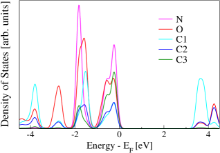
Fig. 2 shows the PDOS for the top layer only. The corresponding pictures for all the following layers do not differ in shape one from another. Although, as described in our previous work they are shifted in the energy, according to the Stark effect.previous The PDOS for all six layers is presented in Fig. S1 in the supporting information. The PDOS analysis indicates, that the electrons and holes localize at different parts of the building molecules. The electrons tend to localize at the central ring, while holes at the dipole terminal groups. This space separation is strongly pronounced for the electrons and light holes, and to some extend for the heavier holes. Similar space separation has been reported for the covalent organic frameworks where two different molecules play the role of acceptor and donor.IHJ
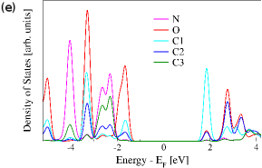
We model the effect of the electrodes on the terminal layers of the optically active material with the graphene sheets. This material is a good candidate for both the cathode and anode, due to its high polarizability and induced change of the work function.previous The hydrogen bonds within the 2D networks are weak, and in fact, there are also possibilities to pattern at graphene without any intermolecular bonding.graphorder ; graf2 Hence, we consider the separated molecular stacks with three different arrangements between the molecules and graphene. The top and side views are presented in Figs. 3(a)-(d). By breaking the planar connections, we gain the additional path for the holes, which now can move between the neighboring carboxy groups. As seen in Fig. 3(e), the application of the graphene electrodes do not affect the electron–hole path separation. The effect of molecular orientation with respect to the graphene axes, as for the cases presented in Figs. 3(a)-(c), turned out to be negligible. The PDOS for all other considered orientations is presented in Fig. S2 in the supporting information.
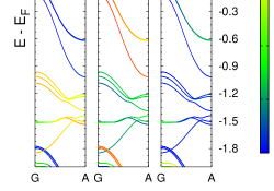
Breaking the planar bonds, as well as addition of the graphene leads, modifies the valence band character. Comparison of Fig. 2 and Fig. 3(e), shows that the top of the valence band in the 2D case (Fig. 2) is built of the states localized at nitrogens and oxygens - which means that the NCCH2- and COOH-group contribute to the states at the same energy below the Fermi level. In contrast, in the 1D case (Fig. 3(e)), the PDOS is built of the oxygen states close to the Fermi level and energetically deeper (around 2-3 eV below the valence band top) nitrogen states. This is a fingerprint of the energetic separation of the light and heavier hole. The same property is exhibited by the infinite 1D molecular stack, for which the band structures projected at the near atomic–centred Wannier functions are shown in Figs. 4(a) and (b) for two lattice constants. The projection onto oxygens (the red color in the middle panel) shows that the contribution of the COOH group is energetically located just below the Fermi level. While the projection to nitrogens (the orange color in the leftmost panel) displays the energetic location of the contribution of the NCCH2 group, which is well below that of the COOH moieties.
The bandwidth is a signature of the carrier mobility, and it is sensitive to the strength of the -orbitals overlap. This can be seen from a comparison of the two above described band structures. The bandwidth of the light hole is about 0.5 eV, for the larger separation between the -rings (Fig. 4(a)), and about 1 eV, for the more closely stacked case (Fig. 4(b)). The heavier hole extends to about 1.4 eV or 1.85 eV for the GGA- or LDA-optimized ring separations, correspondingly. These bandwidths are directly connected to the hole mobilities, which are the derivatives of the energy levels with respect to the lines in the k-space (the change of the point in the Brillouin zone). In other words: fast carriers move along thick bands. The effect of the inter-ring separation for the electron mobilities is less pronounced that that for the holes.
The energy barriers for the rotation of the dipole groups are expected to be small – especially at the elevated temperatures, when the devise is exposed to Sun shine. But in the technological reality, the columnar liquid crystals are densely packed, as well as the columns studied in this work are also placed closely - on the hydrogen bond distance in the 2D case. The 1D model is good enough for the analysis of the mobilities, but the working device will be more similar to the 2D case, where flipping the orientation of the dipole group is not as easy as in the 1D case.
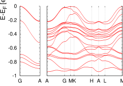
The transport properties of the columnar and planar systems differ too. Therefore, in Fig. 5, we compare the electronic structures of the 1D and 2D systems, including also the model 3D bulk material, which connects the parameters of those two. For the efficient solar cell devices, it is desirable to achieve high conductivity across the layers, whereas insulating properties within the planes – for the purpose of the energy dissipation reduction. Indeed, the band dispersions of the 2D system are very flat with respect to the 1D case. The band gap of the 2D molecular layer is very similar to the HOMO-LUMO gap of an isolated molecule, and decreases with the thickness of the film, to be the smallest for the infinite molecular wire.
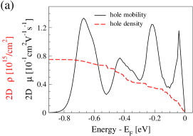
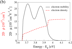
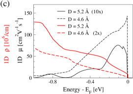
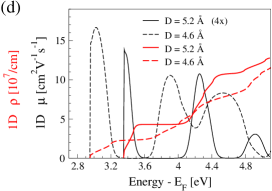
The number of carriers (holes and electrons) per the energetic range decreases for the low dimensional systems. The mobilities are defined as the ratio of the conductivity, proportional to the band dispersion, and the carrier density. This is one of the reasons for the high carrier mobilities obtained in graphene, for example. Figs. 6(a)-(b) present the mobilities obtained for the 2D and Figs. 6(c)-(d) for the 1D molecular system, respectively.
The results for the 1D system are compared for the two intermolecular distances, see Figs. 6(c)-(d). As expected, the carrier mobilities for the 2D case (with molecules connected via the hydrogen bonds) are much lower than these for the 1D system (with the molecules in the -stacking); even at larger (the GGA) lattice constant. This effect is enhanced for the holes, due to the vertical geometry of the dipole groups, which makes the intermolecular distances in the terminal parts smaller than in the central part. On the other hand, the inter–ring distances are equal to the lattice constant of the chain, thus much larger than for instance the interplanar distances in graphite (3.4 ). Decreasing the lattice constant, the electron mobilities grow about 4 times, while the corresponding increase for the holes is about 15 times.
Additionally, in the supporting information, we show the conductivities scaled with the constant relaxation time and plotted for several temperatures, for the 2D and 1D cases; see Figs. S4 and S5 in the supporting information, respectively. For the 2D system, a decrease of the conductivity with the temperature is much more strongly pronounced with respect to the 1D case. Moreover, we observe a visible anisotropy of the hole conductivity along the zigzag and armchair directions in our hexagonal molecular lattice. It is worth to point out, that it is not the case for the electron mobilities.
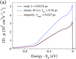
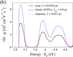
In order to go beyond the mobilities parametrized with the relaxation time, for the 1D infinite molecular column, we estimate the scattering effects according to the elastic and the ionic impurity contributions. We abandon the calculation of the optical-phonons contribution, because in the organic systems this kind of scattering is much lower than that caused by the acoustic phonons.elast ; napht ; srep ; Casian Taking into account only the elastic scattering, the calculated relaxation time for the molecular pillar with the intermolecular distance of 4.6 is 0.36 ps for holes and 0.8 ps for the electrons. These values of correspond to the moblities achieving 5000 cm2V-1s-1 for the holes and 1360 cm2V-1s-1 for the electrons.
In order to calculate the scattering from the ionic impurities, we used the formulae given in the methods section and assumed one ionic impurity with the charge 1 or -1 (which leads to the same result) per ten molecules in the wire (n=0.1/(4.6), =1). The density of free carriers is assumed 1 per the unit cell for the holes and electrons (=1/(4.6)). The relative dielectric constant of our wire was found 1.2 - accoring to the static component of the real part of the dielectric function.eps The calculated relaxation time for the ionic impurity scattering only is 23 fs for the holes and the electrons. Thus, the maximal values of the mobilities achieve 300 cm2V-1s-1 and 39 cm2V-1s-1 for the holes and electrons, respectively.
The ionic scattering takes over the acoustic contribution. Hence, the total relaxation time is 21.6 fs for holes and 22.6 fs for the electrons. The mobilities rescalled according to the obtained relaxation time are printed for holes and electrons in Figs. 7(a) and 7(b), respectively. Concluding, the elastic effects in our molecular wires are compared to these in the organometal halide perovskites.srep The addition of the ionic defects - which are often in the molecular crystalselast ; napht ; penta – drastically increases the scattering and decreases the mobilities. Our analysis shows that, despite the presence of the ionic impurities, the mobilities in our 1D system are high in comparison to other organic systems. The previous works show that the mobilities in some organic materials excess 100 cm2V-1s-1 at low temperatures.mob1 ; mob2 We underline, that the systems studied in this work are highly ordered, which is another reason for the low scattering and it is known that the mobilities in organic crystals are very anisotropic.anisotropy
We compare the mobilities for our systems with these of the organometal halide perovskites.Sanvito ; srep ; Snaith The relaxtion time calculated for our 1D system leads to the mobilities - 300 and 39 cm2V-1s-1 for the holes and electrons, respectively - and these values are larger than for the perovskites. For instance, for CH3NH3PbI3 in the cubic structure, reported in Fig. 4 in Ref. [54], the maximal values for the holes achieve 12 cm2V-1s-1 and 8 cm2V-1s-1 for the electrons - with the assumed relaxation time of 1 ps for the both types of charges. These values agree with the measured mobilities.Snaith However, the other ab initio calculations with the inclusion of the spin-orbit coupling, reported in Table 1 in Ref. [38], lead to largely overestimated values of 1400-2200 cm2V-1s-1 for the holes and 570-800 cm2V-1s-1 for the electrons. The above mobilities were obtained with the same methods which were applied in this study. The relaxation times obtained by Zhao et al.srep are an order of magnitude larger than our values reported in Figs. 7(a) and 7(b). This overestimation results probably from large increase of the bandwidths when the spin-orbit coupling is included and the quasiparticle corrections not.picozzi
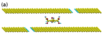
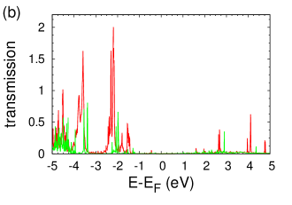
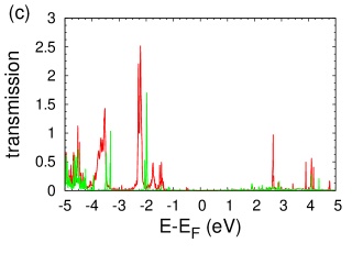
A single molecule sandwiched between the terminated, H-passivated graphene planes is shown in Fig. 8(a). This is the minimal model which represents the -stacking order between the optical spacer (molecules) and the electrodes. The zero-bias transmission function calculations are performed within the GGA and LDA schemes – see Figs. 8(b) and (c), respectively. The two coupling strengths, related to the distances between the molecule and the planes, are considered. The stronger (weaker) coupling corresponds to the case, where the distances are set to 4.6 and 4.0 (5.2 and 4.6 ) for the upper and lower graphene-molecule separations, respectively. The value of the width of the band gap visible in the transmission function stays in a good agreement with the gap size in the PDOS obtained for the molecular stack, see Fig. 3(e). The coupling strength determines the widths of the transmission peaks, i.e. increasing the coupling broadens the peaks. These facts correspond to the discussed mobility features, as well as the band structure derived conclusions. For the weaker coupling cases the positions of the peaks are slightly shifted towards the Fermi energy. This effect is related to the renormalization of the energy levels of the system. The threshold bias for the ’dark current’ is about 3 eV for the holes, while for the electrons it is approximately 2 times higher.
IV Conclusions
We found and discuss the unique transport properties in the -stacked aromatic-rings with the terminal groups possessing the dipole moment – the separate paths for the electrons and holes. This feature could be a solution for the charge recombination problem in the solar cell devices. The electronic diffusion paths cut through the aromatic rings, whereas the holes hop between the neighboring dipole groups. We verified theoretically, that connecting the system to the graphene electrodes does not destroy the above separation. The ferroelectric and path-separation properties are not necessarily directly connected to each other. The driving force for the electron-hole separation is not the dipole moment itself, but the excitonic character of the system - with the donor states at the -electron rich atoms and the acceptor states at the aromatic ring.
The proposed materials can be realized in 2D or 1D, as the layers or molecular wires, correspondingly. For the simplicity, we use the smallest model: one benzene ring, and the cyano groups for the ferroelectric properties, and the carboxy groups for the formation of the hydrogen bonds within the planes. This choice of the planar bonds is dictated by the requirement of a high planar resistance. On the other hand, the carrier mobilities, for the electrons and holes across the layers, respectively, are one and two orders of magnitude larger than the planar ones.
In comparison with the organometal halide perovskites,
reported in Ref. [54], our mobilities along the -stacked
1D columns are an order of magnitude larger for holes and about 5 times
larger for electrons. These values are obtained in the presence
of one charged impurity per ten molecules, which gives large contribution
to the scattering mechanisms.
Supporting Information Description
Further details of the calculations, (S1) DOS projected at groups of atoms indexed in Fig. 1(c),
for each of six monolayers in the AA-type stacking without the leads,
(S2) the same for four monolayers between the graphene leads, (S3) comparison of that for
the first molecular layer in the three stackings: AA-type, R30-deg-type and AB-type,
(S4) conductivity function plots in the 2D case, (S5) the same for the 1D case.
Acknowledgements
This work has been supported by The National Science Centre of Poland
(the Projects No. 2013/11/B/ST3/04041 and DEC-2012/07/B/ST3/03412).
Calculations have been performed in the Cyfronet Computer Centre using
Prometheus computer which is a part of the PL-Grid Infrastructure,
and by part in the Interdisciplinary Centre of
Mathematical and Computer Modeling (ICM).
References
- (1) Rutledge S. A.; Helmy, A. S. Carrier Mobility Enhancement in Poly(3,4-ethylenedioxythiophene)-poly (styrenesulfonate) Having Undergone Rapid Thermal Annealing. J. App. Phys. 2013, 114, 133708.
- (2) Liu, J.; Kim, G. H.; Xue, Y.; Kim, J. Y.; Baek, J. B.; Durstock, M.; Dai, L.. Graphene Oxide Nanoribbon as Hole Extraction Layer to Enhance Efficiency and Stability of Polymer Solar Cells. Adv. Mater. 2014, 26, 786-790.
- (3) Malinkiewicz, O.; Roldán-Carmona, C.; Soriano, A.; Bandiello, E.; Camacho, L.; Nazeeruddin, M. K.; Bolink, H. J. Metal-Oxide-Free Methylammonium Lead Iodide Perovskite-Based Solar Cells: the Influence of Organic Charge Transport Layers. Adv. En. Mater. 2014, 4, 1400345.
- (4) Shkrob, I. A.; Marin, T. W. Charge Trapping in Photovoltaically Active Perovskites and Related Halogenoplumbate Compounds. Chem. Phys. Lett. 2014, 5, 1066-1071.
- (5) Tachikawa, T.; Karimata, I.; Kobori, Y. Surface Charge Trapping in Organolead Halide Perovskites Explored by Single-Particle Photoluminescence Imaging. J. Phys. Chem. Lett. 2015, 6, 3195-3201.
- (6) Stranks S. D.; Snaith, H. J. Metal-Halide Perovskites for Photovoltaic and Light-Emitting Devices. Nature Nanotech. 2015, 10, 391-402.
- (7) Leijtens, T.; Stranks, S. D.; Eperon, G. E.; Lindblad, R.; Johansson, E. M. J.; McPherson, I. J.; Rensmo, H.; Ball, J. M.; Lee, M. M.; Snaith, H. J. Electronic Properties of Meso-Superstructured and Planar Organometal Halide Perovskite Films: Charge Trapping, Photodoping, and Carrier Mobility. ACS Nano 2014, 8, 7147-7155.
- (8) Wang, Y.; Wang, H.-Y.; Yu, M.; Fu, L.-M.; Qin, Y.; Zhang, J.-P.; Ai, X.-C. Trap-Limited Charge Recombination in Intrinsic Perovskite Film and Meso-Superstructured Perovskite Solar Cells and The Passivation Effect of The Hole-Transport Material on Trap States. Phys. Chem. Chem. Phys. 2015, 17, 29501-29506.
- (9) Stranks, S. D.; Burlakov, V. M.; Leijtens, T.; Ball, J. M.; Goriely, A.; Snaith, H. J. Recombination Kinetics in Organic-Inorganic Perovskites: Excitons, Free Charge, and Subgap States. Phys. Rev. Appl. 2014, 2, 034007-8.
- (10) Shi, D.; Adinolfi, V.; Comin, R.; Yuan, M.; Alarousu, E.; Buin, A.; Chen, Y.; Hoogland, S.; Rothenberger, A.; Katsiev, K. et al. Low Trap-State Density and Long Carrier Diffusion in Organolead Trihalide Perovskite Single Crystals. Science 2015, 347, 519-522.
- (11) Milot, R. L.; Eperon, G. E.; Snaith, H. J.; Johnston, M. B.; Herz, L. M. Temperature-Dependent Charge-Carrier Dynamics in CH3NH3PbI3 Perovskite Thin Films. Adv. Funct. Mater. 2015, 25, 6218-6227.
- (12) Xiao, Z.; Yuan, Y.; Yang, B.; VanDerslice, Y.; Chen, J.; Dyck, O.; Duscher, G.; Huang, J. Universal Formation of Compositionally Graded Bulk Heterojunction for Efficiency Enhancement in Organic Photovoltaics. Adv. Mater. 2014, 26, 3068-3075.
- (13) Calik, M.; Auras, F.; Salonen, L. M.; Bader, K.; Grill, I.; Handloser, M.; Medina, D. D.; Dogru, M.; Löbermann, F.; Trauner, D. et al. Extraction of Photogenerated Electrons and Holes from a Covalent Organic Framework Integrated Heterojunction. J. Am. Chem. Soc. 2014, 136, 17802-17807.
- (14) Wuttke, S.; Dietl, C.; Hinterholzinger, F. M.; Hintz, H.; Langhals, H.; Bein, T. Turn-On Fluorescence Triggered by Selective Internal Dye Replacement in MOFs. Chem. Commun. 2014, 50, 3599-3601.
- (15) Dogru, M.; Handloser, M.; Auras, F.; Kunz, T.; Medina, D.; Hartschuh, A.; Knochel, P.; Bein, T. A Photoconductive Thienothiophene-Based Covalent Organic Framework Showing Charge Transfer Towards Included Fullerene. Angew. Chem. Int. Ed. 2013, 52, 2920-2924.
- (16) Dogru, M.; Bein, T. On The Road Towards Electroactive Covalent Organic Frameworks. Chem. Commun. 2014, 50, 5531-5546.
- (17) Tan, Z.-k.; Johnson, K.; Vaynzof, Y.; Bakulin, A. A.; Chua, L.-L.; Ho, P. K. H.; Friend, R. K. Suppressing Recombination in Polymer Photovoltaic Devices via Energy-Level Cascades. Adv. Mater. 2013, 25, 4131-4138.
- (18) Khazaei, M.; Arai, M.; Sasaki, T.; Ranjbar, A.; Liang, Y.; Yunoki, S. OH-Terminated Two-Dimensional Transition Metal Carbides and Nitrides as Ultralow Work Function Materials. Phys. Rev. B 2015, 92, 075411-10.
- (19) Wierzbowska, M.; Wawrzyniak-Adamczewska, M. Cascade Donor-Acceptor Organic Ferroelectric Layers, Between Graphene Sheets, for Solar Cell Applications. eprint 2015, arXiv:cond-mat:1510.05220.
- (20) Sergeyev, S.; Pisula, W.; Geerts, Y. H. Discotic Liquid Crystals: A New Generation of Organic Semiconductors. Chem. Soc. Rev. 2007, 36, 1902-1929.
- (21) Reinert, F. Graphene Gets Molecules Into Order. Nature Phys. 2013, 9, 321-322.
- (22) Zhang, X.; Li, N.; Gu, G.-C.; Wang, H.; Nieckarz, D.; Szabelski, P.; He, Y.; Wang, Y.; Xie, C.; Shen, Z.-Y. et al. Controlling Molecular Growth between Fractals and Crystals on Surfaces. ACS Nano 2015, 9, 11909-11915.
- (23) Medina, D. D.; Rotter, J. M.; Hu, Y.; Dogru, M.; Werner, V.; Auras, F. J. T. Markiewicz, P. Knochel, T. Bein, Room Temperature Synthesis of Covalent–Organic Framework Films through Vapor-Assisted Conversion. J. Am. Chem. Soc. 2015, 137, 1016-1019.
- (24) Zhang, K.-D.; Tian, J.; Hanifi, D.; Zhang, Y.; Sue, A. C.-H.; Zhou, T.-Y.; Zhang, L.; Zhao, X.; Liu, Y.; Li, Z.-T. Toward a Single-Layer Two-Dimensional Honeycomb Supramolecular Organic Framework in Water. J. Am. Chem. Soc. 2013, 135, 17913-17918.
- (25) Horiuchi, S.; Tokura, Y. Organic Ferroelectrics. Nature Mater. (Review), 2008, 7, 357-366.
- (26) Sobolewski, A. L. Organic Photovoltaics Without p–n Junctions: A Computational Study of Ferroelectric Columnar Molecular Clusters. Phys. Chem. Chem. Phys. 2015, 17, 20580-8.
- (27) Horiuchi, S.; Kumai, R.; Tokura, Y. High-Temperature and Pressure-Induced Ferroelectricity in Hydrogen-Bonded Supramolecular Crystals of Anilic Acids and 2,3-Di(2-pyridinyl)pyrazine. J. Am. Chem. Soc. 2013, 135, 4492-4500.
- (28) Horiuchi, S.; Kobayashi, K.; Kumai, R.; Ishibashi, S. Ionic Versus Electronic Ferroelectricity on Donor-Acceptor Molecular Sequence. Chem. Lett. (Highlight Review) 2014, 43, 26-35.
- (29) Giannozzi, P.; Baroni, S.; Bonini, N.; Calandra, M.; Car, R.; Cavvazzoni, C.; Ceresoli, D.; Chiarotti, G. L.; Cococcioni, M.; Dabo, I. QUANTUM ESPRESSO: A Modular and Open-Source Software Project for Quantum Simulations of Materials. J. Phys. Condens. Matter 2009, 21, 395502-19.
- (30) Perdew, J. P.; Burke, K.; Ernzerhof, M. Generalized Gradient Approximation Made Simple. Phys. Rev. Lett. 1997, 78, 1396.
- (31) Mostofi, A. A.; Yates, Y. R.; Lee, Y. S.; Souza, I.; Vanderbilt, D.; Marzari, N. wannier90: A Tool for Obtaining Maximally-Localised Wannier Functions. Comput. Phys. Commun. 2008, 178, 685-699.
- (32) Marzari, N.; Vanderbilt, D. Maximally Localized Generalized Wannier Functions for Composite Energy Bands. it Phys. Rev. B 1997, 56, 12847.
- (33) Marzari, N.; Mostofi, A. A.; Yates, J. R.; Souza, I.; Vanderbilt, D. Maximally Localized Wannier Functions: Theory and Applications. Rev. Mod. Phys. 2012, 84, 1419-1475.
- (34) Pizzi, G.; Volja, D.; Kozinsky, B.; Fornari, M.; Marzari, N. BoltzWann: A Code for The Evaluation of Thermoelectric and Electronic Transport Properties with a Maximally-Localized Wannier Functions Basis. Comp. Phys. Comm. 2014, 185, 422-429.
- (35) Bardeen, J.; Shockley, W. Deformation Potentials and Mobilities in Non-Polar Crystals. Phys. Rev. 1950, 80, 72-80.
- (36) Tang, L.; Long, M.-Q.; Wang, D.; Shuai, Z.-G. The Role of Acoustic Phonon Scattering in Charge Transport in Organic Semiconductors: A First-Principles Deformation-Potential Study. Sci. China Ser. B-Chem. 2009, 52, 1646-1652.
- (37) Wang, L. J; Peng, Q.; Li, Q. K.; Shuai, Z. G. Roles of Inter- and Intramolecular Vibrations and Band-Hopping Crossover in The Charge Transport in Naphthalene Crystal. J. Chem. Phys. 2007, 127, 044506.
- (38) Zhao, T.; Shi, W.; Xi, J.; Wang, D.; Shuai, Z. Intrinsic and Extrinsic Charge Transport in CH3NH3PbI3 Perovskites Predicted from First-Principles. Scientific Reports 2015, 6, 19968.
- (39) Casian, A.; Dusciac, V.; Coropceanu, Iu. Huge Carrier Mobilities Expected in Quasi-One-Dimensional Organic Crystals. Phys. Rev. B 2002, 66, 165404.
- (40) Jurchescu, O. D.; Baas, J.; Palstra, T. T. M. Effect of Impurities on The Mobility of Single Crystal Pentacene. Appl. Phys. Lett. 2004, 84, 3061-3063.
- (41) Chattopadhyay, D.; Queisser, H. J. Electron-Scattering by Ionized Impurities in Semiconductors. Rev. Mod. Phys. 1981, 53, 745-768.
- (42) QuantumESPRESSO. www.quantum-espresso.org (accessed March 10, 2016).
- (43) Ordejón, P.; Artacho, E.; Soler, J. M. Self-Consistent Order-N Density-Functional Calculations for Very Large Systems. Phys. Rev. B, 1996, 53, R10441.
- (44) Soler, J. M.; Artacho, E.; Gale, J. D.; García, A.; Junquera, J.; Ordejón, P.; Sánchez-Portal, D. The SIESTA Method for Ab Initio Order-N Materials Simulation. J. Phys. Condens. Matter 2002, 14, 2745.
- (45) Brandbyge, M.; Mozos, J. L.; Ordejón, P.; Taylor, J.; Stokbro, K. Density-Functional Method for Nonequilibrium Electron Transport. Phys. Rev. B 2002, 65, 165401.
- (46) Hohenberg, P.; Kohn, W. Inhomogeneous Electron Gas. Phys. Rev., 1964, 136, B864.
- (47) Kohn, W.; Sham, L. J. Self-Consistent Equations Including Exchange and Correlation Effects. Phys. Rev. 1965, 140, A1133.
- (48) Ceperley, D. M.; Alder, B. J. Ground State of the Electron Gas by a Stochastic Method. Phys. Rev. Lett. 1980, 45, 566.
- (49) Wehrenfennig, C.; Eperon, G. E.; Johnston, M. B.; Snaith, H. J.; Herz, L. M. High Charge Carrier Mobilities and Lifetimes in Organolead Trihalide Perovskites. Adv. Mater. 2014, 26, 1584-1589.
- (50) Colson, J. W.; Woll, A. R.; Mukherjee, A.; Levendorf, M. P.; Spitler, E. L.; Shields, V. B.; Spencer, M. G.; Park, J.; Dichtel, W. R. Oriented 2D Covalent Organic Framework Thin Films on Single-Layer Graphen. Science 2011, 332, 228-231.
- (51) Sakanoue, T.; Sirringhaus, H. Band-Like Temperature Dependence of Mobility in a Solution-Processed Organic Semiconductor. Nat. Mater. 2010, 9, 736-740.
- (52) Karl, N.; Kraft, K.-H.; Marktanner, J.; Münch, M.; Schatz, F.; Stehle, R.; Uhde, H.-M. Fast Electronic Transport in Organic Molecular Solids. J. Vac. Sci. Technol. A 1999, 17, 2318-2328.
- (53) de Wijs, G. A.; Mattheusa, C. C.; de Groot, R. A. Palstra, T. T. M. Anisotropy of The Mobility of Pentacene from Frustration. Synth. Met. 2003, 139, 109-114.
- (54) Motta, C.; Mellouhi, F. E.; Sanvito, S. Charge Carrier Mobility in Hybrid Halide Perovskites. Sci. Rep. 2015, 5, 12746.
- (55) Bokdam, M.; Sander, T.; Stroppa, A.; Picozzi, S.; Sarma, D. D.; Franchini, C.; Kresse, G. Role of Polar Phonons in the Photo Excited State of Metal Halide Perovskites. eprint 2015, arXiv:cond-mat/1512.05593.