Electric coupling in scanning SQUID measurements
Abstract
Scanning SQUID is a local magnetometer which can image flux through its pickup loop due to DC magnetic fields (). Scanning SQUID can also measure a sample’s magnetic response to an applied current () or voltage () using standard lock-in techniques. In this manuscript, we demonstrate that electric coupling between the scanning SQUID and a back gate-tuned, magnetic sample can lead to a gate-voltage dependent artifact when imaging or . The electric coupling artifact results in and images which mimic the spatial variation of the static magnetic fields from the sample (e.g. ferromagnetic domains). In back-gated bilayers, we show that the electric coupling effect is important, and is responsible for the reported signal from chiral currents in Wang et al. [1]. Previous scanning SQUID current imaging experiments are unaffected by this artifact, as they are either on non-magnetic samples or the spatial distribution of magnetism does not match the features observed in . In conclusion, or imaging of magnetic, back-gated samples should only be applied and interpreted with great caution.
Note: A retraction of Ref. [1] will appear in Science on December 18th, 2015. Here we explain in detail the reasons for the retraction.
1 Executive Summary
In Ref.[1], written by several of us, scanning superconducting quantum interference devices (SQUID) were used to investigate the magnetic domain structure and current flow in bilayers. A back gate voltage was used to tune the chemical potential of the . At negative gate voltages, images of flux from current applied to the sample () showed features which were interpreted as signatures of domain wall currents associated with the quantum anomalous Hall effect (QAHE). The signal in (from written magnetic domain structure) scaled with the local voltage of the sample, rather than the current, which was interpreted as evidence of the current’s chiral nature.
In the section 2, Sample-SQUID electric coupling model, we derive a model for electric coupling between the SQUID and sample, which leads to an artifact in and imaging when the sample is back-gated and magnetic. The charge of the back-gated device is modulated when a voltage is applied to the sample. The charge of the sample couples electrically to the grounded metal on the SQUID itself. The electric coupling causes the height of the SQUID’s pickup loop above the sample to oscillate when an oscillating voltage or current is applied to the sample. In the presence of magnetic fields from the sample, the gradient of the local magnetic field is coupled into the and images by the oscillation of the SQUID. We simulated images from both chiral currents and the electric coupling artifact, which is proportional to the height derivative of the magnetic image (). The images from chiral currents and the electric coupling artifact are qualitatively very similar, although the electric coupling artifact is noticeably sharper.
In section 3, Experimental signatures of electric coupling in , we compare the theoretical predictions of the electric coupling artifacts to new measurements of the field, frequency, and back gate voltage dependencies of magnetic images of bilayers. We found that current and voltage images ( and ) match the expected features of the electric coupling artifact. Specifically, we imaged and found that the sign of the signal reverses sign as a function of frequency and back gate voltage, and the signal disappears when the SQUID is in contact with the sample. These features are not consistent with a signal from chiral currents along domain walls.
Based on these measurements, we’ve reevaluated the images in Ref. [1] in Implications for Ref. [1] (section 4). We show that the detailed spatial dependence of images taken by Wang et al. along the edge of a device (Fig. 2 in Ref. [1]) very closely matches the height derivative of the magnetic image (), as expected for electric coupling. We also show previously unpublished data taken by Wang et al., showing that the features observed in Fig. 2 disappear halfway through a scan, suggesting that the SQUID is in contact. Additionally, sign reversal of features as a function of back gate are shown for a written domain.
The results of the new measurements and the presence of strong evidence for the electric coupling artifact in measurements performed for Ref. [1] lead to the conclusion that the results of Ref. [1] are primarily, if not completely due to electric coupling, rather than chiral currents.
Finally, in Electric coupling in other current imaging experiments (section 5) we briefly comment on other works where scanning SQUID was used to image current, and describe why the electric coupling artifact present in SQUID measurements are not responsible for the features observed in those works ([2, 3, 4]).
2 Sample - SQUID electric coupling model
2.1 Model of electric coupling
Scanning SQUID is a sensitive local flux to voltage converter. The SQUID’s pickup loop is brought very close to a sample and scanned in order to image magnetic fields. Our SQUIDs also have a field coil which is concentric with the pickup loop, and can be used to apply a local field. Our SQUID devices are fabricated on silicon chips, which are polished close to the pickup loop in order to bring it very close to the sample (typically within a few microns).
Our scanning SQUID chip is typically mounted on a copper cantilever (FIG.1 a) for scanning. We detect a deflection of this cantilever capacitively when the SQUID chip touches the sample, which gives us topographic imaging of the sample. We can either scan with the SQUID ”in contact” with the tip of the polished SQUID chip touching the sample, or ”out of contact” which means that the SQUID’s tip scans above the sample.
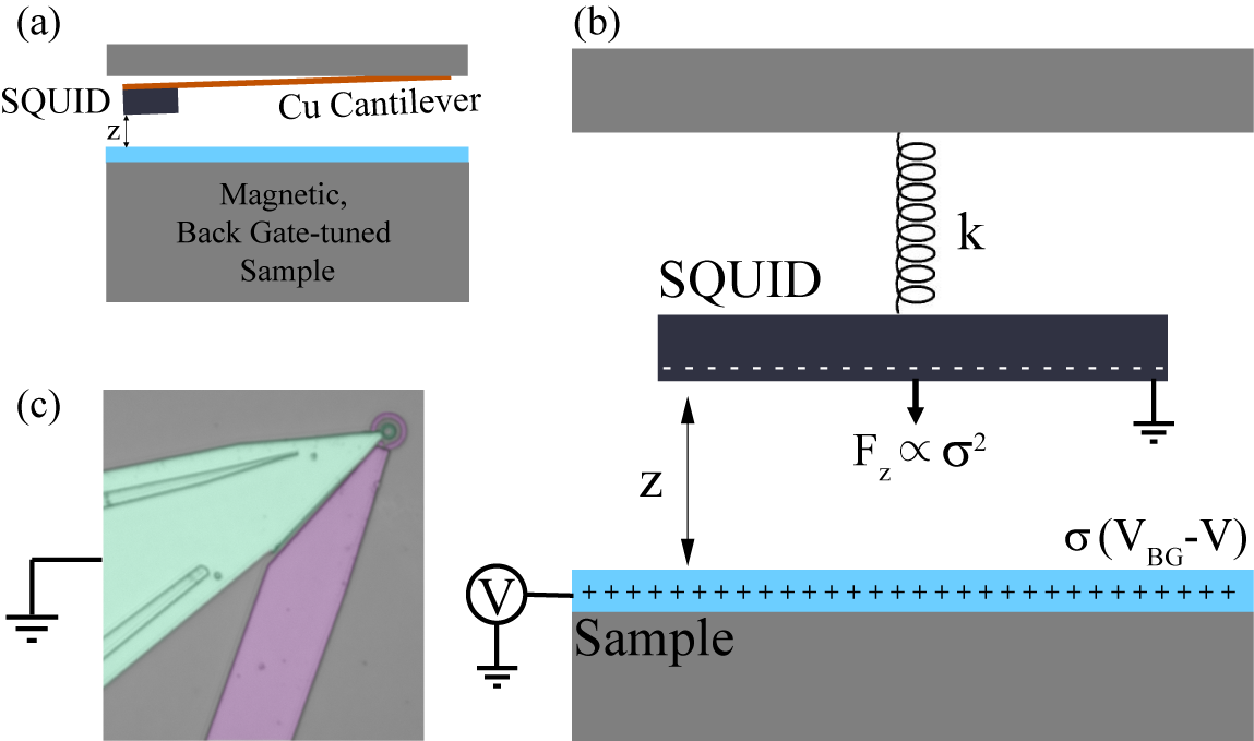
When the SQUID is out of contact it is free to vibrate or deflect if a force is applied to it. We modeled the coupling between grounded metal on the SQUID and the charge on a gated sample (FIG. 1 b). The tip of the scanning SQUID (FIG. 1 c) has a pickup loop with superconducting shielding (green) and a field coil which also has shielding (purple). Both loops and their shielding are grounded during normal operation of the SQUID. A charge on the sample will exert a force on a grounded metallic SQUID. The Coulomb force will lead to a deflection of the SQUID which depends on the charge accumulated on the sample.
The following model is very similar to how charge is measured in electric force microscopy, however the amount of charge on the sample itself is also modulated by a voltage.
A generic electric equation for the force on the grounded SQUID due to a gated semiconducting sample with a voltage applied to the sample is:
| (1) |
where ,, and are parameters with the appropriate units which depend on the SQUID and sample geometry, is the 2D charge density induced in the semiconductor by a back gate, is the voltage applied to the sample, is the voltage applied to the back gate, and is the contact potential difference.
The first term is the force between the charged sample and a grounded metallic object, and this is the term which is relevant for this paper. This force will be proportional to the square of the induced charge on the sample. A second term, which is present due to the applied voltage difference between the sample and SQUID, leads to a term which goes as . The contact potential difference (is a term which is important for Kelvin Probe Force microscopy [5], for example) is typically less than 1 V in magnitude.
The back gate acts as a parallel plate capacitor with the sample and back gate as the plates. Therefore, the induced charge density on the sample will be proportional to , leading to the second equality in Eqn. 1. For a lock-in measurement, we are only concerned with terms linear in V when we are measuring the 1st harmonic. If is small, the second term goes primarily as and will only show up in 2nd and higher harmonics. For the purposes of this discussion we will ignore this term, but it can in principle also lead to other artifacts.
We can now balance the electric force with the restoring force of the cantilever
| (2) |
Where k is the spring constant of the cantilever and is its equilibrium position. Solving for , we find:
| (3) |
Again, since we only are concerned with terms linear in V for lock-in measurements, we can drop the first two terms and find the first harmonic of the response to a sinusoidal excitation:
| (4) |
We have now established, for a back-gated sample with an induced charge and a grounded SQUID, that the application of a sinusoidal voltage excitation to the sample can lead to a sinusoidal height variation of the SQUID. This height variation directly couples the gradient of any DC magnetic fields in the sample into a lockin measurement of the SQUID’s response.
By applying a voltage to the sample and measuring the SQUID’s response, we are measuring the constant component of . The full measured , taking into account the above height variation is:
| (5) |
The first term is the true change in the flux from the sample due to the applied voltage, for example from a chiral current which is modulated by gate voltage or from voltage-induced domain wall motion. The second term is the ’electric coupling artifact’ term due to linear coupling of the height of the SQUID to the applied voltage, which is the main result of this section.
Similarly, if we want to measure , there is an electric coupling term. Flowing a current in a resistive sample leads to a voltage drop across the sample. The local voltage of the sample near the SQUID will induce a coupling to the height of the SQUID. The strength of the electric coupling () however, will vary as a function of position along the sample and the sample’s resistance. In our model, the electric coupling at a fixed position will be proportional to R, ().
The electrostatic model established here is simplistic. We have not included a realistic model of the actual form of the electric coupling, or the frequency dependence of the response of the cantilever. The electric coupling , depends on the geometry and distance between the SQUID and sample and the screening from the sample itself. As the sample becomes more conducting, the screening of the back gate induced charge will decrease the electric coupling coefficient, which in the case of means that the electric coupling artifact will be diminished at positive gate voltages, where the sample is more conducting. Additionally, the resonance of the cantilever will also lead to a mechanical resonance-like response in the strength and sign of the electric coupling artifact.
In conclusion, the robust predictions of the electric coupling model presented here are that the electric coupling signal will be proportional to , it will change sign as a function of back gate voltage, and it will also be proportional to the mechanical response (and any resonances) of the cantilever.
2.2 Signals due to chiral currents and electric coupling are qualitatively similar
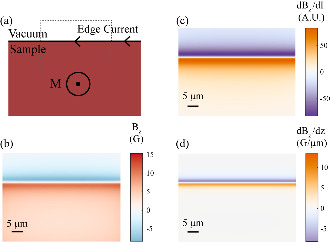
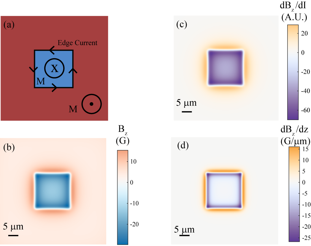
In the quantum anomalous Hall state, chiral currents flow along the edges of devices and at domain walls [6]. The magnetic fields (specifically the out of plane component, ) from chiral currents should be spatially resolvable by scanning SQUID microscopy. We simulated the expected images due to currents along the edge of a device and at the wall of a written magnetic domain, and then compared them to the simulated image due to the electric coupling artifact derived above. We find that they are qualitatively similar, and therefore great caution must be exercised in attempting to measure chiral currents in samples with magnetic structure using scanning SQUID.
We simulated images of the expected signals at the edge of a sample with a uniform out-of-plane polarization (FIG. 2) and around a written domain (FIG. 2). The expected signal from current flowing along the edge of the sample (2 c) is qualitatively reproduced by the electric coupling artifact, (FIG. 2 d). Similarly, the current flowing along the domain wall of a written domain (FIG. 3 c) looks qualitatively similar to the electric coupling artifact, (FIG. 3 d).
The spatial dependence of the chiral current images and the electric coupling images are different in the details. The chiral current and magnetic field images for out of plane domains, however, are identical up to an overall scaling factor for the geometries we’ve simulated (FIG. 3 b and c). Therefore, comparing images of to both and gives us another way of discriminating between real chiral current signals and electric coupling artifacts.
In the following section, we will use the SQUID-sample coupling model to show that electric coupling is dominant in new measurements we’ve performed on .
3 Experimental signatures of electric coupling in
Here we will give four pieces of evidence that strongly indicate that the electric coupling term is dominant in our new measurement of bilayers. We argue that all of the signals observed in this measurement of and are due to electric coupling. The four pieces of evidence are:
All of these effects are easily understandable in the model presented above, and hard to reconcile with a signal that arises due to chiral currents along magnetic domain walls and edges.
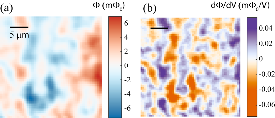
Typical DC magnetometry () and images are presented in FIG. 4. We measured the sample as-cooled, with no external field applied at any point during the cooling process. We focused on a 30 x 30 area of the device. We found ferromagnetic domain structure in DC magnetometry, the size of which is mostly limited by the SQUID’s spatial resolution (FIG. 4 a). At large negative (), we observe a large signal in . The spatial pattern of is very similar to the domain structure observed in the image (FIG. 4 b).
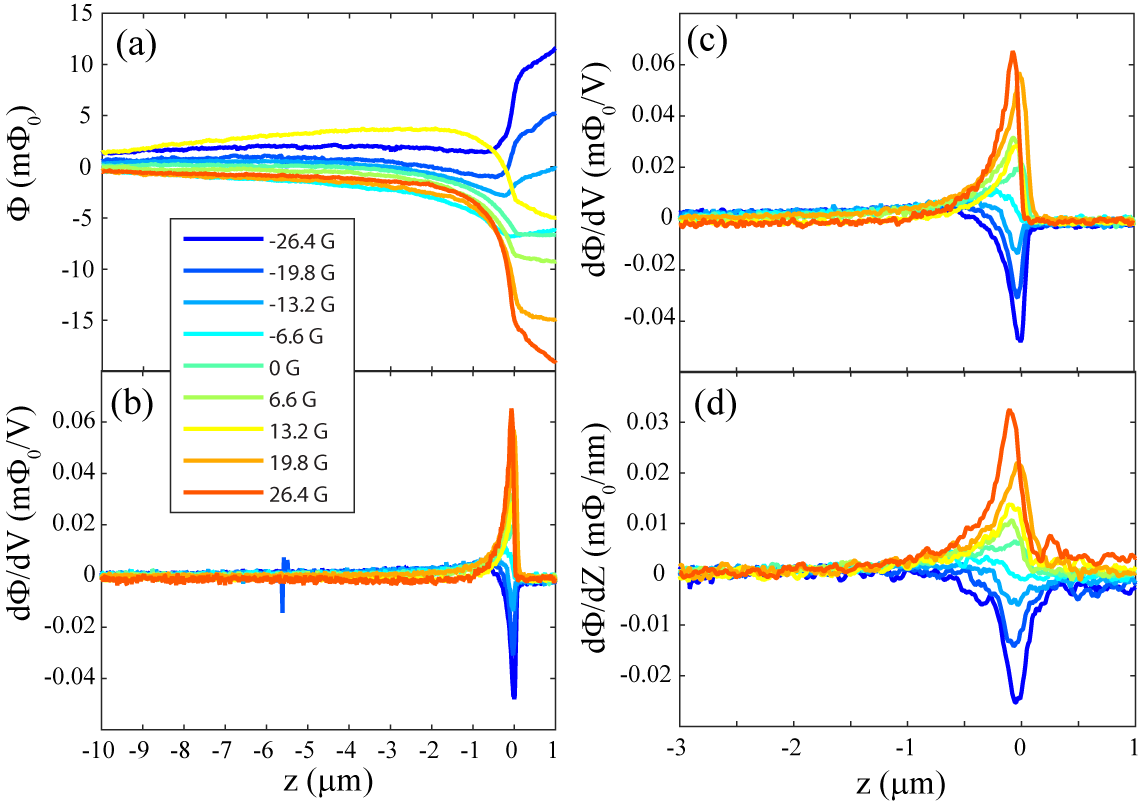
To investigate the signal in a different way, we measured the dependence of and on height above the sample (FIG. 5 a & b). At a fixed gate voltage and temperature ( & ) we measured and and changed the applied out-of-plane field (). (FIG. 5 a) is tuned by the field by changes in the domain structure and the paramagnetic response of the sample. We found that appears to be much more sharply varying than and that goes to zero when the SQUID is in contact with the sample.
The electric coupling term in Eqn. 5 is directly proportional to , so we took the numerical derivative of with respect to height in order to compare the two. We applied a smoothing filter (over z) to before taking a numerical derivative, in order to more clearly see the qualitative features. We found that the shape and dependence on field of qualitatively matches that of (Fig. 5 c & d ). Specifically, both are significantly sharper than and are strongly reduced while in contact with the sample.
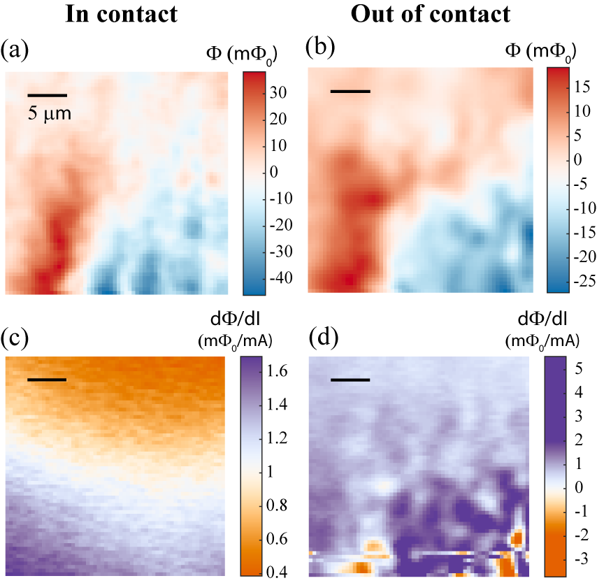
The sharp height dependence of and its similarity to corresponding curves are suggestive that electric coupling is responsible for the observed signal. The disappearance of when the SQUID is in contact with the sample is, we believe, a strong piece of evidence that the signal is indeed the electric coupling artifact. To further investigate this, we imaged of in and out of contact (FIG. 6).
When the SQUID’s chip is in contact with the sample, we expect the electrically-induced vibration of the SQUID to be strongly damped due to the restoring force of the sample itself. We imaged both in contact and out of contact (FIG. 6 a & b). The only difference between in contact and out of contact is the sharpness of images, which is because magnetic field lines spread as distance from the sample increases. The images both in contact and out of contact (FIG. 6 c & d) are qualitatively different. Out of contact, (FIG. 6 d), we primarily observed a similar structure to what is observed in (FIG. 4 b). However, when we imaged in contact (FIG. 6 c) the magnetic domain-like features completely disappear. We were left only with a plane-like spatial dependence, consistent with homogeneous current flow in the device.
The stark difference in the measured in and out of contact makes sense if the magnetic-domain like signals in are due to electric coupling. In the magnetic domain-like feature disappear in contact as well (as we showed in height dependence, FIG. 5). Additionally, the apparent lack of any domain-like signal while the SQUID is in contact shows that there is no measurable signal from chiral currents in this particular image.
Another explanation for the in contact behavior could be that the voltage applied to the sample is shorted to the SQUID. We checked this possibility by putting the SQUID in contact with the sample while applying a DC voltage and measuring leakage. We did not observe any leakage current from the sample to ground, indicating that shorting was not an issue in this measurement. The presence of an insulating layer on top of the sample () makes shorting unlikely. In previous experiments on top-gated samples, we have observed shorting of a couple of volts to the SQUID, and in these cases we were unable to successfully take SQUID images due to the shorting. These problems were not present in measurements, indicating that shorting was most likely not occurring while imaging.
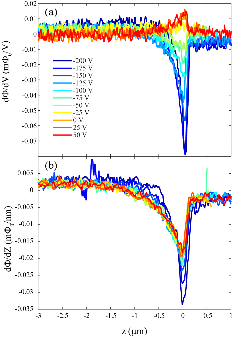
We compared and as a function of to further corroborate the electric coupling explanation. In order to maximize the observed signal, we applied an out of plane field = -26.4 G. Looking back at Eqn. 5, we expect the electrically-induced vibration, and therefore the electric coupling term in to change sign with . We measured and as a function of (FIG. 7) and found that while varied strongly and ultimately flipped sign at positive , varied considerably less. The relative sign between and changed between = 0 and -25 V., which is consistent with what we predicted in Eqn. 5. The fact the sign of changes at a non-zero indicates that the heterostructure’s flat band voltage is non-zero, which is plausible.
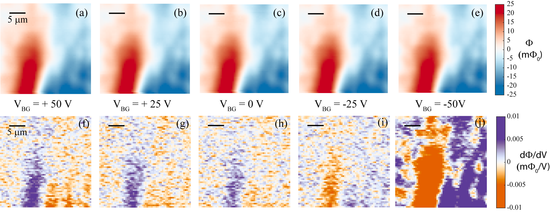
The sign change of is predicted by electric coupling, but inconsistent with a chiral current explanation. We further showed this by taking images at many around zero voltage in zero applied field (FIG. 8). We found that the DC magnetic features remained constant (FIG. 8 a-e), while the relative sign of the features in flipped between = 0 and -25 V. As grown is strongly n-doped, so the presence of any chiral current features near = 0 V is highly unlikely, but the sign flip of the features is inconsistent with a signal from chiral currents.
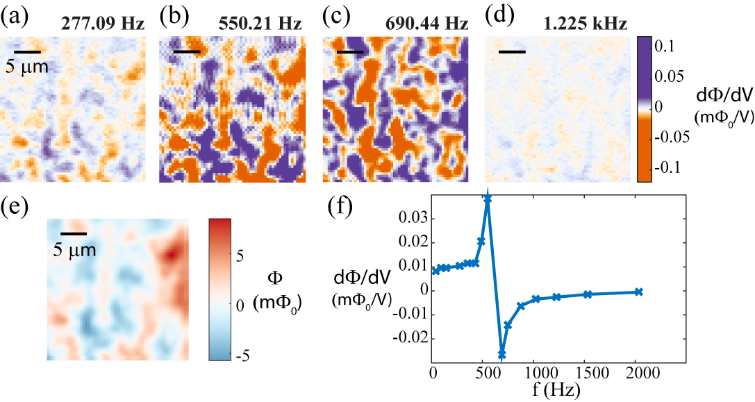
Finally, we also observed that the features in flipped sign as a function of the frequency of the voltage excitation (FIG. 9). The features in images (FIG. 9 a-d) match the domain structure observed in (FIG. 9 e), however the features in flipped sign around f=600 Hz. To further show the frequency dependence, we plotted the value in the bottom left corner of this area at many frequencies (FIG. 9 f). We found signal’s sign flipped and its magnitude peaked at f Hz.
The frequency dependence of strongly indicates a mechanical resonance of the SQUID’s cantilever. In our derivation of the electric coupling we assumed static forces, and therefore did not take any mechanical resonance of the cantilever into account. A resonance leads to a frequency dependence which would also affect the magnitude and sign of and therefore the electric coupling term in . We roughly estimated the resonance of our Cu cantilever using Copper’s room temperature values for the Young’s modulus (E = 130 GPa) and density (), and approximate size of the cantilever’s thickness and length ( & L = 10 mm). We calculated 600 Hz, close to the measured resonance.
We have performed careful height, field, frequency, and dependencies of and and compared them to predictions for the derived trivial electric coupling term. The disappearance of the magnetic-domain like signal in and in contact, and the sign flips of the observed signals as a function of frequency and are all easy to explain by electric coupling and extremely hard to reconcile with a signal from chiral currents along domain walls.
4 Implications for Ref. [1]
We have demonstrated in the previous section that electric coupling is completely responsible for the observed and images in a new measurement on bilayers. We will now analyze the images obtained in the studies that led to Ref. [1] and argue that they are also caused by electric coupling, rather than chiral currents.
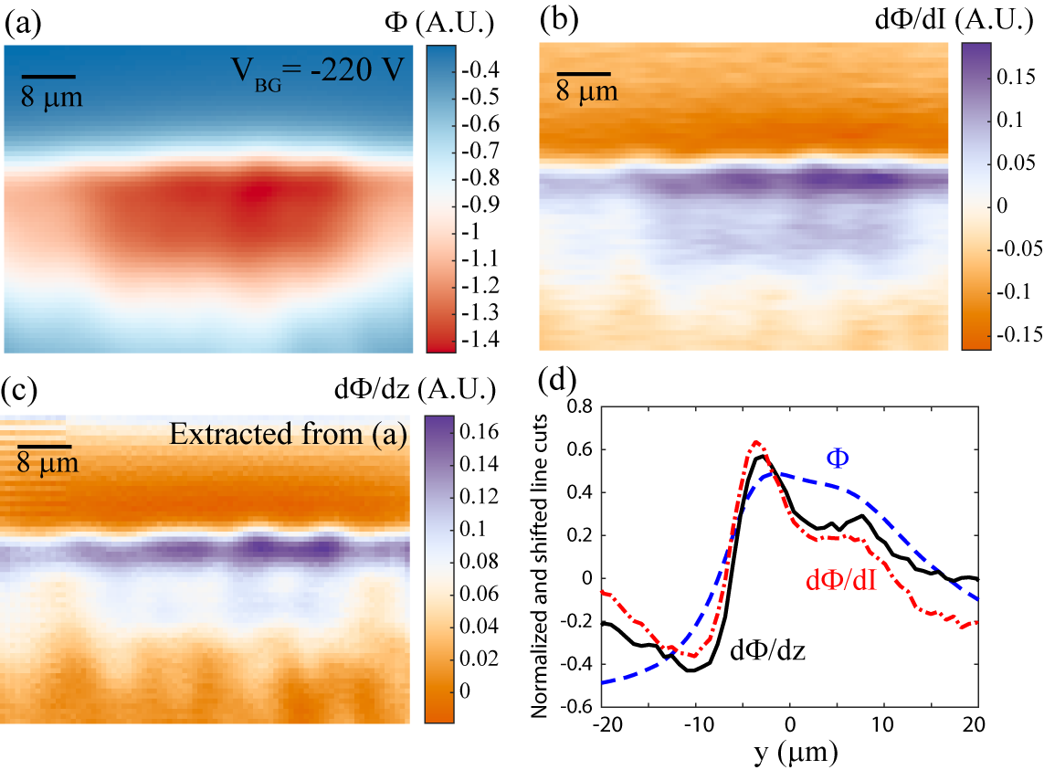
We will first show that the images from Ref. [1] match very closely the spatial dependence expected for the electric coupling artifact () by propagating the images in height. Specifically, we have reproduced Fig. 2 B & E from Ref. [1] in FIG. 10 a & b.
In order to extract from a single magnetometry image, we utilized Fourier techniques to propagate the magnetic image up in height:
| (6) |
Where FFT and IFFT are the 2D fast Fourier transform and its inverse, k is the magnitude of the spatial frequency , is the height of the SQUID above the sample, and is the height we have propagated the magnetic image [7].
In order to get , we then subtract the two images:
| (7) |
We found that the extracted image (FIG. 10 c) is nearly identical to the spatial structure in the measured image (FIG. 10 b). This is strongly suggestive evidence that the observed signal in Ref. [1] is due to electric coupling.
From simulations (see FIG. 2 & 3), we found that the spatial dependence of a chiral current signal more closely matches the spatial dependence of the magnetic fields from an out of plane domain, rather than its height derivative. Specifically, for out-of-plane domains, the magnetic fields from a fully polarized domain are equivalent to a current flowing along the edge of the domain. This is a generalization of , where is the magnetic dipole moment of a small dipole, and is the current flowing in a loop of area .
The spatial dependence of the image presented in Ref. [1] is nearly identical to what we expect for electric coupling (), and is sharper than the magnetic fields we naively expect for chiral currents along the edge of an out of plane polarized domain structure. Line cuts of the images (FIG. 10 d) further show the similarity between the simulated and .
Next, we will look at unpublished data that was taken in the same cooldowns as the results presented in Ref. [1]. We show that two of the main pieces of evidence for electric coupling in the new measurements are also present in those data sets. Specifically, the images observed in Ref. [1] also disappear while the SQUID is in contact, and signals of reversed sign are observed at large positive back gate voltages for written domains.
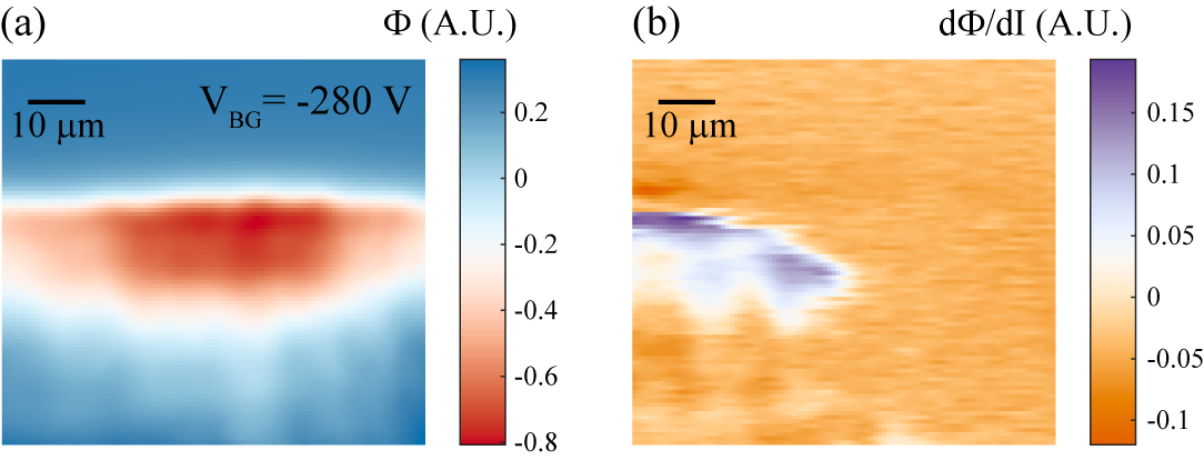
Taken in sequence with the other gate voltage images shown in Fig. 2 of [1], an image was taken at = -280 V, where goes to zero for a large portion of the scan (FIG. 11). This disappearance of during the scan was previously interpreted as an inhomogeneous back gate voltage distribution in the sample before an equilibrium of charge distribution was reached. However, a more likely explanation for this effect is that the signal disappears in contact, and that the SQUID is touching the sample for the right half of the image.
The right side of FIG. 11 b shows that while the SQUID is contact, there is no observable signal indicating an edge current. This indicates that not only is the electric coupling artifact present in these measurements, but that it accounts for all of the signal observed in the left half of the scan.
In combination with the effects described in previous section, we have also observed in multiple cooldowns that the voltage applied to the piezo-positioner which is required to touch the sample with the SQUID varies as a function of . We found that the SQUID seems to ’snap to’ the sample at large negative gate voltages. In other words, a DC electric force leads to height variation for images taken with nominally the same parameters. We believe that this effect, in combination with the disappearance of the signal when the SQUID is in contact, can explain the lack of a signal observed at . Images of the same sample, in the same cooldown, show strong signals in at a similar back gate voltage ( ), showing that it is likely that Fig.2F from Ref. [1] was taken in contact with the sample.
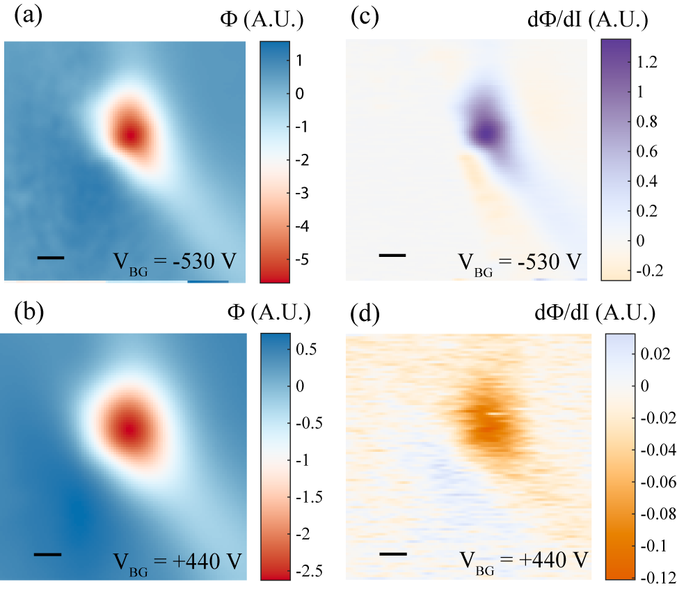
A sign reversal of the signal was observed between large negative and positive gate voltages in unpublished measurements by Wang, et al. on domain structure written with the field coil (FIG. 12). Domain structure was written by applying an inhomogeneous DC magnetic field with the field coil, similar to what was done for Fig. 4 in Ref. [1]. The sign of the signal switched between large negative and positive back gate voltages (FIG. 12 c & d). This is inconsistent with a signal from chiral currents, and can be explained by the electric coupling artifact.
The signal at large positive was significantly weaker than at large negative , roughly a factor of 20 for bias voltages applied to the same end of the sample. The asymmetry in signal size is not predicted by our simple model. Multiple factors can in principle contribute to the asymmetry, including height differences between the scans, differences in the actual applied local voltage due to contact resistance, differences in the screening length, and the contribution of a true chiral current signal at negative gate voltages. The asymmetry is also observed at lower gate voltages in the new measurements, where we have ruled out the presence observable chiral current signals by scanning in contact. Therefore we believe the asymmetry does not require the presence of chiral currents. The large difference in signal size can be accounted for by taking into account screening and height.
For Fig. 12, we estimate that the difference in size of due to induced height differences between negative and positive gate voltages is 3 by the looking at calculated images. In Fig. 8, we observed a factor of 5 difference between positive and negative gate voltages. At low voltages, we do not observe a large height shift in images (FIG. 8 a-e), so we attribute this factor of 5 mainly to screening effects. Therefore, height and screening effects contribute a lower bound of a factor of 15 to the asymmetry between positive and negative gate voltage images, which is close to the observed factor of 20.
We have shown that the signal observed in Ref. [1] is consistent with a signal that is due to electric coupling between the SQUID and the device. The measured current image at the edge of the sample very closely matches the extracted image, and is naively ’too sharp’ to match the expected spatial variation expected for chiral currents. We also found evidence that the signal in unpublished measurements done in the same experiments as Ref. [1] disappeared when the SQUID was in contact, and flipped sign between negative and positive back gate voltages.
Taken together with the electric coupling model developed in this paper and the new measurements performed on , we have shown that the signals reported in Ref. [1] are dominated by electric coupling and show no clear evidence of chiral currents.
5 Electric coupling in other current imaging experiments
Scanning SQUID has been utilized to measure and reconstruct current densities in , HgTe quantum wells, and InAs/GaSb quantum wells ([2, 3, 4]). In HgTe and InAs/GaSb, we observed current along the edges of the devices for certain top gate voltages. In , we observed that the more current flowed along features due to the tetragonal domain structure of STO. The electric coupling effect described above cannot explain the main observations of those papers for a number of reasons.
Most important, there were no features in which match the observed current features in any of the previous scanning SQUID results. The electric coupling artifact produces features in or which qualitatively match the signal observed in . If the samples are non-magnetic ( = 0, and therefore = 0), then the electric coupling term in Eqn. 5 also goes to zero. In both HgTe and InAs/GaSb, there were no observed features in . In , some of the observed samples were magnetic, as discussed in [8], however this magnetism occurred in resolution-limited magnetic dipoles, which does not match the quasi 1D features observed in .
Additionally, in both HgTe and InAs/GaSb the gates are top gates rather than back gates, which significantly changes the electric field environment. Both top and back gates modulate the charge on the device itself, but the metallic top gate is between the grounded SQUID and the sample, which will strongly screen the charge on the sample from the SQUID, resulting in an extreme reduction electric coupling.
6 Conclusion
In conclusion, electric coupling between the SQUID and sample can lead to an electric coupling artifact in a specific type of measurement and sample. Specifically, and measurements of back-gated semiconducting samples with magnetic features. Any SQUID measurements of this type should be very strongly scrutinized. The electric coupling effect is present and the dominant signal in our new measurements of , and can also explain all of the observations of Ref. [1].
If the sample is non-magnetic or top-gated, or the measurements are not or , the electric coupling effect described here will not be relevant.
7 Acknowledgments
We acknowledge Christopher Watson for useful discussions. These measurements and analysis were supported by the Department of Energy, Office of Science, Basic Energy Sciences, Materials Sciences and Engineering Division, under Contract DE-AC02-76SF00515. Earlier measurements were supported both by FAME, one of six centers of STARnet, a Semiconductor Research Corporation program sponsored by MARCO and DARPA, and by the Department of Energy, Office of Science, Basic Energy Sciences, Materials Sciences and Engineering Division, under Contract DE-AC02-76SF00515. The SQUID microscope and sensors were developed with support from NSF-NSEC 0830228 and NSF IMR-MIP 0957616. Y.H.W. was partially supported by the Urbanek Fellowship of the Department of Applied Physics at Stanford University. For sample preparation, F.K., P. J-H., and J.S.M. would like to thank support by the MIT MRSEC through the MRSEC Program of the National Science Foundation under award number DMR-0819762. Partial support for sample development was provided by NSF (DMR-1207469), ONR (N00014-13-1-0301) (F.K. and J.S.M.) and by the DOE, Basic Energy Sciences Office, Division of Materials Sciences and Engineering, under Award No. DE-SC0006418 (F.K. and P. J-H.).
References
- [1] Y. H. Wang, J. R. Kirtley, F. Katmis, P. Jarillo-Herrero, J. S. Moodera, and K. A. Moler, “Observation of chiral currents at the magnetic domain boundary of a topological insulator,” Science, vol. 349, no. 6251, pp. 948–952, 2015.
- [2] B. Kalisky, E. M. Spanton, H. Noad, J. R. Kirtley, K. C. Nowack, C. Bell, H. K. Sato, M. Hosoda, Y. Xie, Y. Hikita, et al., “Locally enhanced conductivity due to the tetragonal domain structure in heterointerfaces,” Nature Materials, vol. 12, no. 12, pp. 1091–1095, 2013.
- [3] K. C. Nowack, E. M. Spanton, M. Baenninger, M. König, J. R. Kirtley, B. Kalisky, C. Ames, P. Leubner, C. Brüne, H. Buhmann, et al., “Imaging currents in hgte quantum wells in the quantum spin hall regime,” Nature Materials, vol. 12, no. 9, pp. 787–791, 2013.
- [4] E. M. Spanton, K. C. Nowack, L. Du, G. Sullivan, R.-R. Du, and K. A. Moler, “Images of edge current in quantum wells,” Phys. Rev. Lett., vol. 113, p. 026804, Jul 2014.
- [5] M. Nonnenmacher, M. P. O’Boyle, and H. K. Wickramasinghe, “Kelvin probe force microscopy,” Applied Physics Letters, vol. 58, no. 25, 1991.
- [6] J. Wang, B. Lian, and S.-C. Zhang, “Quantum anomalous hall effect in magnetic topological insulators,” Physica Scripta, vol. 2015, no. T164, p. 014003, 2015.
- [7] B. J. Roth, N. G. Sepulveda, and J. P. Wikswo, “Using a magnetometer to image a two-dimensional current distribution,” Journal of Applied Physics, vol. 65, no. 1, pp. 361–372, 1989.
- [8] J. A. Bert, B. Kalisky, C. Bell, M. Kim, Y. Hikita, H. Y. Hwang, and K. A. Moler, “Direct imaging of the coexistence of ferromagnetism and superconductivity at the interface,” Nature Physics, vol. 7, no. 10, pp. 767–771, 2011.