Tunable skewed edges in puckered structures
Abstract
We propose a new type of edges, arising due to the anisotropy inherent in the puckered structure of a honeycomb system such as in phosphorene. Skewed-zigzag and skewed-armchair nanoribbons are semiconducting and metallic, respectively, in contrast to their normal edge counterparts. Their band structures are tunable, and a metal-insulator transition is induced by an electric field. We predict a field-effect transistor based on the edge states in skewed-armchair nanoribbons, where the edge state is gapped by applying arbitrary small electric field . A topological argument is presented, revealing the condition for the emergence of such edge states.
pacs:
71.30.+h, 73.22.-f, 73.63.-bI Introduction
Recently black phosphorus attracts much attention since the experimental demonstration of a field-effect transistor (FET).li14 Several experimental and theoretical papers appeared in the last year, which has demonstrated its properties and potential applications. rodin14 ; liu14 ; gomez14 ; xia14 ; qiao14 ; koenig14 Graphene is not viable for post-silicon electronics due to the lack of a band gap, while the band gap of black phosphorus can be tuned by changing the number of layers or applying an electric field.gomez14 ; rudenko14 ; kim15 Black phosphorus could potentially serve a whole range of purposes for FET, while retaining higher electron mobility than transition-metal dichalcogenides.
The graphene analogue of black phosphorus is phosphorene, liu14 ; rudenko14 a monolayer sheet of phosphorus atoms arranged in a honeycomb lattice. The structure of phosphorene is puckered, where the emergence of distinct zigzag ridges leads to highly anisotropic properties. While the majority of research is focused on bulk phosphorene, low14 ; cakir14 ; yuan15 ; pereira15 ; chaves15 ; tahir15 ; srivastava15 it is of interest to analyze the properties of phosphorene nanoribbons.peng14 ; du15 ; carvalho14 Zigzag graphene nanoribbons have zero-energy edge states, while armchair ones can be semiconducting or metallic, depending on their width.nakada96 ; fujita96 ; ezawa06 Recently, it was shown that a similar picture holds true for phosphorene nanoribbons, where zigzag nanoribbons host a quasi-flat band detached from the bulk, corresponding to edge states near the Fermi level,ezawa14 while armchair nanoribbons are semiconducting, and become metallic under a sufficiently strong electric field. sisakht15 ; guo14
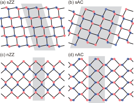
In this paper, we propose a new type of edges in the anisotropic honeycomb lattice system without the rotational symmetry. Phosphorene is the best example. On the one hand, the planar honeycomb structure has the rotational symmetry. On the other hand, only the symmetry exists in the puckered structure due to the anisotropy, which allows us to introduce a new type of zigzag or armchair edges. In particular, we may cut the honeycomb sheet so that the zigzag (armchair) direction intersects the puckered ridges under an angle other than (), as illustrated in Fig. 1(a) and (b). We refer to these nanoribbons as skewed-zigzag (sZZ) and skewed-armchair (sAC) nanoribbons. These are a new type of edges. In contrast we refer to the normal nanoribbons as normal-zigzag (nZZ) and normal-armchair (nAC) nanoribbons, as shown in Fig. 1(c) and (d). By calculating the band structure, we find that the sZZ nanoribbons are semiconducting while the sAC nanoribbons are metallic. Namely we have found an unexpected duality between a set of the skewed edges and a set of the normal edges: If the normal nanoribbon is metallic, the skewed one is insulating, and vice versa. This duality has a topological origin. We next show that the properties of these skewed edges are electrically tunable. First, an electric field along the width of the nanoribbon can close (open) the band gap in sZZ (sAC) nanoribbons. Second, it is remarkable that an arbitrarily small electric field perpendicular to the sheet, obtainable by vertical gating, can open a band gap in sAC nanoribbons. It would become an insulator under mVÅ at room temperature for phosphorene. This is not the case for nZZ nanoribbons, where band gap opening is possible only for certain nanoribbons subjected to extremely large fields. Although we use phosphorene as an explicit example, our arguments are applicable to any materials with anisotropic nearest neighbor hoppings.
II Band Structure
The tight-binding model is adequate to elucidate the new physics of the puckered system. It helps us to capture the essential physics irrespective of material details. The model Hamiltonian reads
| (1) |
where are parameters describing the hopping between the lattice sites and , while is the on-site energy induced by the electric field. We show the lattice structure of nanoribbons in Fig. 1. Note that the sZZ (sAC) direction is not parallel (normal) to the puckered ridges which are shown by red and blue disks. It is convenient to define the width of the normal (skewed) nanoribbon by one half (quarter) of the number of atoms in the unit cell, which we denote also by or ( or ) appropriately. For each nanoribbon we perform a Fourier transform to the momentum basis, diagonalize the corresponding Hamiltonian, and obtain in the band structure.
To display explicitly the band structure we employ the tight-binding Hamiltonian derived recently by Rudenko et al. for phosphorene,rudenko15 which contains hopping parameters up to the site separation Å. It reproduces well the band structure near the Fermi level.
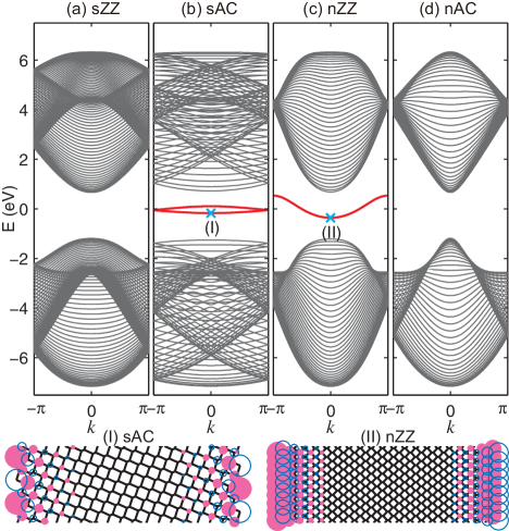
Typical band structures of sZZ, sAC, nZZ and nAC nanoribbons are shown for the case of width in Fig. 2. On the one hand, no edge states are present and a large band gap is opened in the sZZ nanoribbon. This is highly contrasted to the nZZ nanoribbon [Fig. 2(d)], where there are edge-localized states.ezawa14 In this sense, the band structure of the sZZ nanoribbon resembles that of the nAC nanoribbon.sisakht15 On the other hand, two quasi-flat bands (QFBs) appear in the middle of the band gap for the band structure of the sAC nanoribbon, as shown in Fig. 2(b). It is analogous to the nZZ nanoribbon [Fig. 2(c)]. Indeed, it is possible to verify topologically that QFBs in the sAC nanoribbon share the same topological origin as QFBs in the nZZ nanoribbon.
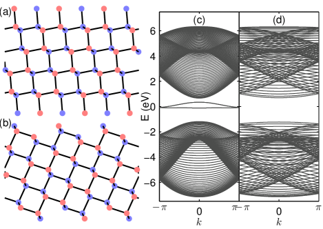
A comment is in order with respect to another set of edges. Interestingly, adding one neighboring atom to the outermost atoms along the edge, turns skewed-zigzag (armchair) nanoribbon into a skewed-bearded (dangled) nanoribbon, with (without) quasi-flat bands. Most likely, these nanoribbons are unstable and prone to passivization, but are nevertheless important in providing insight into the anisotropic honeycomb nanoribbon model. In Fig. 3(a) and (b) we show the real space layout of these nanoribbons. The band structures of such nanoribbons are shown in Fig. 3(c) and (d), respectively. Note that they are virtually identical to the band structures of the related nanoribbons they are derived from, apart from the fact that now edge states appear when they were not present before, and vice versa.
III Topological Arguments
We reveal the topological origin of the emergence and the absence of edge states. The essential structure of the anisotropic honeycomb lattice is given by the Hamiltonian,ezawa14
| (2) |
with
| (3) |
where three independent parameters and describe the three nearest neighbor hoppings. It agrees with the Hamiltonian (1) up to the nearest neighbor hopping, which is sufficient to capture the underlying physics.
Caution is needed when we analyze a nanoribbon. First, it is necessary to set for the normal edge, and for the skewed edge. Second, although the phase of the function is arbitrary for the honeycomb sheet, it is to be fixed so as to make the coefficient of real for the outermost link according to the type of the edge.ryu ; ezawa14 We thus use
| (4) |
for the nZZ and sZZ edges, and
| (5) |
for the nAC and sAC edges.
The momentum along the nanoribbon is a good quantum number. Hence we consider a one-dimensional insulator indexed by , which may be topological or not. If it is topological for all , the edge is gapless due to the bulk-edge correspondence ryu for all these one-dimensinal insulators. Consequently we have predicted the emergence of a perfect flat band in the Hamiltonian (2). It is deformed into a realistic QFB when hoppings beyond the nearest neighbor ones are included.ezawa14
The topological number is defined by the loop integral along the momentum orthogonal to the nanoribbon ryu ; ezawa14 ,
| (6) |
where with and for the nZZ and sZZ edges, while with and for the nAC and sAC edges.
The phase should be fixed as follows. For the general zigzag edge we have
| (7) |
while for the general armchair edge we have
| (8) |
For the general beard edge we have
| (9) |
while for the general dangled edge we have
| (10) |
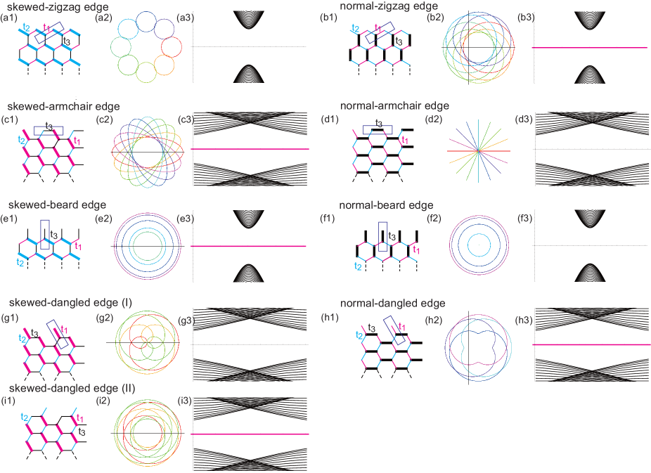
The winding number can be obtained geometrically. The winding number counts how many times the phase of surrounds the origin. We find that the loop is formed in the Re-Im[] plane as a function of . If the loop encircles the origin, , while if the loop does not encircle the origin, . The results are shown in Fig. 4(a2), (b2), (c2) and (d2). Alternatively, we can explicitly evaluate the winding number using the residual theorem of the complex function, which are summarized in the following.
III.1 Zigzag edge
For the zigzag edge, by inserting (7) into (6) and setting , the winding number is rewritten as
| (11) |
A pole exists at
| (12) |
The residual integral gives for and for .
Hence, the condition of the emergence of the edge states is explicitly given by , or
| (13) |
since
| (14) |
For the skewed-zigzag edge, by setting , this condition is simplified as
| (15) |
It is equals to
| (16) |
There is no solution for when , or . In conclusion, edge states do not emerge for in the skewed-zigzag edge as shown in Fig. 4(a3).
For the normal zigzag edge, by setting , this condition is simplified as
| (17) |
A solution exists for all when . In conclusion, a perfect flat band emerges for in the normal-zigzag edge as shown in Fig. 4(b3).
III.2 Armchair edge
For the armchair edge, by inserting (8) into (6) and setting , the winding number is rewritten as
| (18) |
Poles exist at
| (19) |
We find
For the skewed-armchair edge, by setting , two poles satisfies and for . In conclusion, perfect flat bands emerge for in the skewed-armchair edge as shown in Fig. 4(c3).
For the normal armchair edge, by setting , we find for since and for and and for . In conclusion, edge states do not emerge for in the normal armchair edge as shown in Fig. 4(d3).
To summarize, the topological number (6) for each type of nanoribbon, for all with , we find
| (20) |
It manifests the duality that the existence and absence of the edge states are opposite in the skewed and normal nanoribbons. Note that our topological arguments are applicable to any materials with anisotropic nearest neighbor hoppings with the condition in (2). Furthermore, we would like to stress that the topological nature of edge states in phosphorene is not the same as edge states in conventional 2D topological insulators. In particular, the edge states in phosphorene are less robust, and more sensitive to disorder.
IV Lateral Gating
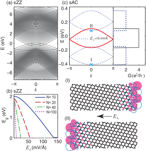
It is a standard technique to employ an electric field to control the band gap. We start with a discussion on the effects of lateral gating. We can close the band gap of sZZ nanoribbons by applying an electric field along the nanoribbon width [Fig.5(a)]. Due to a large Stark effect, the conduction (valence) bands are shifted downwards (upwards) in energy, resulting in an insulator-metal transition.
The critical field is smaller for wider nanoribbons due to the following two reasons: i) wider nanoribbons experience larger potential variation along the width direction due to the field, making them more sensitive to smaller fields; ii) the band gap of wider nanoribbons in the absence of external fields is smaller, and asymptotically approaches the bulk band gap for wide enough naroribbons, which is eV for phosphorene.rudenko15 These two effects are illustrated in Fig. 5(b) for and .
In Fig. 5(c) we take a closer look at the QFBs under an applied electric field . One can see that sAC nanoribbons can be transformed into an insulator by lateral gating since the two-fold degenerate edge states split into opposite directions, thus breaking the double degeneracy. The wave functions become localized at the nanoribbon edge for the occupied and unoccupied QFB, as shown in the panels (I) and (II), respectively. The conductances are switched off, which implies that sAC nanoribbons act as an FET by .
V Vertical Gating
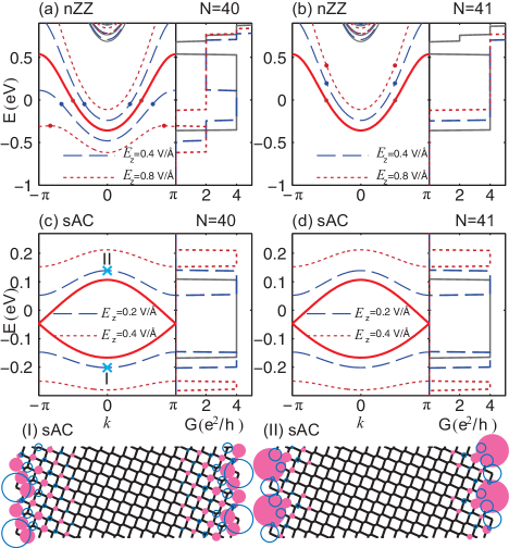
We proceed to investigate the effects of the electric field perpendicular to the honeycomb sheet (). First we analyze nZZ nanoribbons. In Fig. 6 we show the band structure, and the corresponding conductance of (a) and (b) nanoribbons, for (black full curves), V/Å(blue dotted curves) and V/Å(red dashed curves). Intriguingly, we find that the behavior near the Fermi level at half filling (depicted by a dot) depends crucially on the parity of .
When is an even number, the two outermost ridges of the nanoribbon, which support most of the weight of the edge states, belong to different sublayers. Therefore, applying will differentiate the two degenerate QFBs, and split them into opposite directions. For a sufficiently strong an energy gap appears between the two bands, and since only the lower band is filled at half-filling, this constitutes an FET action. The critical field is high ( mV/Å), which is independent of the width, unless the nanoribbons are very narrow. The reason for such a high critical field is the relatively large bandwidth of the QFBs. The edge state at the momentum is almost localized at the outermost ridge, while the wave function penetrates into the bulk as reaches . Accordingly, the shift of the energy at is maximum and that at is minimum.
On the other hand, if is an odd number, the outermost ridges exist in the same plane as shown in Fig.1 (c). Accordingly, both bands of the edge states shift in the same direction by applying , keeping the degeneracy intact, as can be seen in Fig. 6(b). Hence, a gap cannot be induced by at half-filing. Namely it is necessary that is even to make a FET. Furthermore, an extremely large electric field is necessary to open a gap, which is an obstacle for FET operation.
Finally we analyze sAC nanoribbons. In Fig. 6(c) and (d) we depict the band structure of and nanoribbons, respectively. One can see that opens a band gap, by shifting the conduction (valence) band up (down). The double degeneracy of the folded bands are preserved, which is evident from the conductance. The corresponding edge states with finite become predominantly localized on the upper (lower) sublayer, as shown in panels (I) and (II) of Fig. 6. Accordingly, the edge states corresponding to the positive-curvature (electron-like) valence bands move to lower energy, while those corresponding to the negative-curvature (hole-like) conduction bands move to higher energy. Hence, the electric field separates the electron- and hole-like states and bands apart. This is the Stark effect. Importantly, a gap opens under arbitrarily small electric field. We find mVÅ in order to open a gap corresponding to the room temperature. Moreover, note that there are no parity issues in sAC nanoribbons; they all respond in the same manner to an external electric field, regardless of the width. In conclusion, sAC nanoribbons may well be suited for practical devices.
VI Discussion and the Conclusion
In our analysis we have assumed atomically precise edges, about which we make a few comments. (i) Structural relaxation and the effect of dangling bonds can be properly treated by means of first-principles calculations. Previous first-principles calculations have shown guo14 that the quasi-flat bands are robust for pristine normal nanoribbons when taking into account the structural relaxation and dangling bonds. We might expect that our results are also valid for pristine nanoribbons. (ii) Edge states will emerge when there are some regions whose edges are locally precise although the global edge structure is disordered. Indeed, edge states of graphene have been observed even when the edge is not perfectly precise. tao11 (iii) With respect to the impact of the electric field, the shift of the QFB will be robust in the presence of disorder since it is due to the total imbalance of the upper and lower electron distribution, which is independent of the details of the edge roughness.
We also comment on the numerical values such as the critical electric field we have derived for phosphorene. Since they are derived based on the tight-binding model, they can be modified by first-principles calculations. Nevertheless, our results give an order of magnitude estimate, which will benefit future experimental works.
In conclusion, we have proposed a new type of edges, the sZZ and sAC edges, that can appear in puckered honeycomb systems, and revealed intriguing properties inherent to nanoribbons possessing these edges. The sAC nanoribbon is particularly interesting, since it has QFBs whose origin is topological, and since a gap opens by applying an arbitrary small electric field . This property may allow a FET to be designed.
Acknowledgements.
This work was supported by the Serbian Ministry of Education, Science and Technological Development, and the Flemish Science Foundation (FWO-Vl). M.E. thanks the support by the Grants-in-Aid for Scientific Research from MEXT KAKENHI (Grant Nos. 25400317 and 15H05854).References
- (1) L. Li, Y. Yu, G. J. Ye, Q. Ge, X. Ou, H. Wu, D. Feng, X. Hui Chen, and Y. Zhang, Nature Nanotech. 9, 372 (2014).
- (2) A. S. Rodin, A. Carvalho, and A. H. Castro Neto, Phys. Rev. Lett. 112, 176801 (2014).
- (3) H. Liu, A. T. Neal, Z. Zhu, Z. Luo, X. Xu, D. Tománek, and P. D. Ye, ACS Nano 8, 4033 (2014).
- (4) A. Castellanos-Gomez, L. Vicarelli, E. Prada, J. O. Island, K. L. Narasimha-Acharya, S. I. Blanter, D. J. Groenendijk, M. Buscema, G. A. Steele, J. V. Alvarez, H. W. Zandbergen, J. J. Palacios, and H. S. J. van der Zant, 2D Materials 1, 025001 (2014).
- (5) F. Xia, H. Wang, and Yichen Jia, Nat. Commun. 5, 4458 (2014).
- (6) J. Qiao, X. Kong, Z.-X. Hu, F. Yang, and W. Ji, Nat. Commun. 5, 4475 (2014).
- (7) S. P. Koenig, R. A. Doganov, H. Schmidt, A. H. Castro Neto, and Barbaros Özyilmaz, Appl. Phys. Lett. 104, 103106 (2014).
- (8) A. N. Rudenko and M. I. Katsnelson, Phys. Rev. B 89, 201408 (2014).
- (9) J. Kim, S. S. Baik, S. H. Ryu, Y. Sohn, S. Park, B.-G. Park, J. Denlinger, Y. Yi, H. J. Choi, and K. S. Kim, Science 349, 723 (2015).
- (10) T. Low, R. Roldán, H. Wang, F. Xia, P. Avouris, L. M. Moreno, and F. Guinea, Phys. Rev. Lett. 113, 106802 (2014).
- (11) D. Çakir, H. Sahin, and F. M. Peeters, Phys. Rev. B 90, 205421 (2014).
- (12) S. Yuan, A. N. Rudenko, and M. I. Katsnelson, Phys. Rev. B 91, 115436 (2015).
- (13) J. M. Pereira Jr. and M. I. Katsnelson, Phys. Rev. B 92, 075437 (2015).
- (14) A. Chaves, T. Low, P. Avouris, D. Çakir, and F. M. Peeters, Phys. Rev. B 91, 155311 (2015).
- (15) M. Tahir, P. Vasilopoulos, and F. M. Peeters, Phys. Rev. B 92, 045420 (2015).
- (16) P. Srivastava, K. P. S. S. Hembram, H. Mizuseki, K.-R. Lee, S. S. Han, and S. Kim, J. Phys. Chem. C 119, 6530 (2015).
- (17) X. Peng, A. Copple, and Q. Wei, J. Appl. Phys. 116, 144301 (2014).
- (18) Y. Du, H. Liu, B. Xu, L. Sheng, J. Yin, C.-G. Duan, and X. Wan, Sci. Rep. 5, 8921 (2015).
- (19) A. Carvalho, A. S. Rodin, and A. H. Castro Neto, Europhys. Lett. 108, 47005 (2014).
- (20) K. Nakada, M. Fujita, G. Dresselhaus, and M. S. Dresselhaus, Phys. Rev. B 54, 17954 (1996).
- (21) M. Fujita, K. Wakabayshi, K. Nakada, and K. Kusakabe, J. Phys. Soc. Jpn. 65, 1920 (1996).
- (22) M. Ezawa, Phys. Rev. B, 73, 045432 (2006)
- (23) M. Ezawa, New. J. Phys. 16, 115004 (2014).
- (24) E. T. Sisakht, M. H. Zare, and F. Fazileh, Phys. Rev. B 91, 085409 (2015).
- (25) H. Guo, N. Lu, J. Dai, X. Wu, and X. Cheng Zeng, J. Phys. Chem. C 118, 14051 (2014).
- (26) A. N. Rudenko, S. Yuan, and M. I. Katsnelson, Phys. Rev. B 92, 085419 (2015).
- (27) S. Ryu and Y. Hatsugai, Phys. Rev. Lett. 89 077002 (2002).
- (28) C. Tao, L. Jiao, O. V. Yazyev, Y.-C. Chen, J. Feng, X. Zhang, R. B. Capaz, J. M. Tour, A. Zettl, S. G. Louie, H. Dai, and M. F. Crommie, Nat. Phys. 7, 616 (2011).