Electronic structures and theoretical modelling of two-dimensional group-VIB transition metal dichalcogenides
Abstract
Atomically thin group-VIB transition metal dichalcogenides (TMDs) have recently emerged as a new class of two-dimensional (2D) semiconductors with extraordinary properties including the direct band gap in the visible frequency range, the pronounced spin-orbit coupling, the ultra-strong Coulomb interaction, and the rich physics associated with the valley degree of freedom. These 2D TMDs exhibit great potentials for device applications and have attracted vast interest for the exploration of new physics. 2D TMDs have complex electronic structures which underlie their physical properties. Here we review the bulk electronic structures in these new 2D materials as well as the theoretical models developed at different levels, along which we sort out the understandings on the origins of a variety of properties observed or predicted.
1School of Physics, Beijing Institute of Technology, Beijing 100081, China
2Department of Physics and Center of Theoretical and Computational Physics, The University of Hong Kong, Hong Kong, China
3Department of Physics, Carnegie Mellon University, Pittsburgh, Pennsylvania 15213, USA
4Department of Physics, University of Washington, Seattle, Washington, USA
5Department of Material Science and Engineering, University of Washington, Seattle, Washington, USA
∗Corresponding author, wangyao@hku.hk
1 Introduction
Atomically thin two-dimensional (2D) forms of layered transition metal dichalcogenides (TMDs) have recently attracted remarkable scientific and technological interest.1, 2, 3, 4 These TMDs have the chemical composition of MX2, where M stands for the transition metal elements and X for the chalcogen elements. They exhibit a wide range of material properties, for example, NbS2, NbSe2, TaS2, TaSe2, -MoTe2, and Td-WTe2 are metals in bulk form,5, 6, 7, 8 while ReS2, ZrS2, MoS2, WS2, MoSe2, WSe2, and -MoTe2 are semiconductors.5, 6, 2, 9, 10 Their layered bulk structure is the stacking of monolayers by weak van der Waals like forces, and the realization of the 2D forms are promised by the in-plane stability of monolayers provided by the strong covalent bonds. Among the various TMDs, the group-VIB ones (MMo, W; XS, Se) have been most extensively studied in 2D forms, where both the monolayers and few-layers are proved to be stable in air under room temperature4. Each monolayer is an X-M-X covalently bonded hexagonal quasi-2D lattice (cf. Fig. 1), similar to graphene. Atomically thin group-VIB TMDs (monolayers, bilayers, etc.) have been prepared in a number of ways, including mechanical exfoliation from bulk crystals,1, 11, 12, 13 chemical vapor deposition,14, 15, 16, 17 and molecular beam epitaxy.18, 19 Group-VIB TMDs are attracting great interest as a new class of semiconductors in the 2D limit, having remarkable electronic and optical properties.20, 21
A number of extraordinary properties associated with the unique quantum degrees of freedom of electrons have been discovered in 2D group-VIB TMDs.21 The conduction and valence bands have degenerate extrema (i.e. valleys) located at the and points of the hexagonal Brillouin zone (BZ) (cf. Fig. 1c). In particular, monolayers are found to have a direct band gap at these valleys,11, 12 where the optical transitions have a valley dependent selection rule: interband transitions at () valley couple exclusively to the right- (left-) circularly polarized light.22, 23 This optical selection rule makes possible quantum control of the valley pseudospin, including the demonstrated optical generation and detection of valley polarization24, 25, 26 and valley coherence.27 Moreover, the valley pseudospin is associated with the valley Hall effect that makes possible its electric control,28, 23, 29 and the valley magnetic moment for possible magnetic control.28, 30, 31, 32 Similar to spin, these valley phenomena allow the potential use of valley pseudospin for information processing. In bilayers, electrically tunable properties of the valley pseudospin and the strong interplay between the valley pseudospin with the real spin and the layer pseudospin have also been discovered.33, 34, 35 2D group-VIB TMDs could provide the platform to explore these various quantum degrees of freedom of the electrons for future electronic devices with versatile functionalities.
Because of the direct band gap in the visible frequency range, monolayer group-VIB TMDs are ideal systems to explore optoelectronic phenomena and applications in the truly 2D limit. The elementary excitation key to many optoelectronic phenomena is the exciton, a hydrogen-like bound state formed by a pair of electron and hole. Under finite doping, this neutral excitation can bind an extra electron or hole to form a charged exciton, and such a three-particle bound state is also known as a trion. Recent experiments show that excitonic physics can be remarkably interesting in 2D group-VIB TMDs. Photoluminescence (PL) measurements have demonstrated the continuous evolution from positively charged, to neutral, and then to negatively charged excitons as a function of doping controlled by gate.36, 37, 27 First-principles calculations have shown the exotic nature of excitons in 2D group-VIB TMDs: a strong binding energy of hundreds of meV, and a wave function largely of the Wannier type (i.e. extended over a large number of unit cells).38, 39 The calculated binding energy agrees in orders of magnitude with recent experiments based on optical reflection spectra,40 two-photon absorption spectra,41, 42, 43, 44 and scanning tunneling microscopy and spectroscopy.45, 46 The exceptionally large binding energy and the electrostatic tunability of excitons in 2D group-VIB TMDs strongly suggest a new paradigm for the study of exciton physics. Moreover, they imply a particularly strong Coulomb interaction in 2D group-VIB TMDs due to the reduced dielectric screening in the 2D geometry,39, 42 which will lead to interesting many-body phenomena.
Remarkable progresses have been made in devices based upon 2D group-VIB TMDs. Monolayer MoS2 field effect transistors at room temperature have shown high current on/off ratios, low standby power dissipation and reasonably good mobility, which significantly promoted the interest in these 2D materials for device applications.13 Various approaches in fabrication of high quality 2D TMD transistors have led to the steady progress in improving the mobilities in these devices.47, 48, 49, 50, 51 Light-emitting - junctions have also been created electrostatically within TMD monolayers by independent gating adjacent regions of the layer.52, 53, 54, 55 Ambipolar transport in these devices are clearly demonstrated, and electroluminescence in the forward biased - junction has been observed. Interestingly, the electroluminescence from some devices is found to be circularly polarized, possibly a manifestation of unbalanced light emissions from the two valleys controlled by electric gating.55, 56
Nanostructures in 2D group-VIB TMDs are also being actively explored, including nano-flakes,57, 58 nano-ribbons,59, 60, 61, 62, 63, 64, 65, 66, 67, 68, 69, 70 grains and grain boundaries,16, 17, 71 lateral heterostructures,71 and quantum dots.72, 73 In particular, on smooth edges or domain boundaries of TMD monolayers and bilayers, mid-gap metallic states are found with large density of states.57, 58, 16, 19 These metallic states are catalytically active for hydrodesulfurization and hydrogen evolution reaction, and nano flakes of 2D group-VIB TMDs are of high interest for these catalytic applications. 74, 75, 76, 77, 78, 79, 80, 81, 82, 83, 84, 19
The above are only a few selected examples of the appealing features of 2D group-VIB TMDs, which are being discovered at a rapid pace. They have made these 2D materials an ideal platform to explore a variety of applications, as well as an excellent building block for van der Waals heterostructures that may lead to even richer physics.4
Underlying the extraordinary properties of 2D group-VIB TMDs are their electronic structures. While 2D group-VIB TMDs are widely considered as the gapped counterpart of graphene with the same hexagonal 2D lattice, the electronic structures are much more complicated. At least a total of eleven atomic orbitals in each unit cell – five -orbitals from the metal atom and six -orbitals from the two chalcogen atoms – are considered relevant in various contexts. The strong spin-orbit coupling (SOC) inherited from the -orbitals introduces more complexity as well as interesting spin-dependence in the electronic and optical properties. Unlike graphene where a single-orbital tight-binding (TB) model well describes the electronic structure of the active bands over the entire BZ, theoretical models have been developed for 2D group-VIB TMDs at different levels with their advantages and limitations, owning to the complex electronic structures. Momentum space models aim at describing the low energy electrons and holes near the band edges in the 2D bulk, and the real space TB models are indispensable for calculations of mesoscopic transport as well as the study of nanostructures such as quantum dots and nano-ribbons. Models involving more atomic orbitals may give better description of the bands over larger -space regions, while simpler models that capture the essential physics are advantageous in the theoretical studies of complex phenomena. In light of the rapidly growing research activities, a review that gives a comprehensive account of the electronic structures and the theoretical models in 2D group-VIB TMDs, sorting out the origin of the observed extraordinary properties, is necessary.
This review will focus mainly on the development in the theoretical understanding of electronic structures in the 2D bulk of group-VIB TMDs including the band dispersions, electronic and optical band gaps, the spin-orbit splitting and spin/pseudospin configurations of the energy bands, the orbital compositions and symmetries of the wave functions, the selection rules for the optical inter-band transition, interlayer hopping, heterojunctions, as well as the Berry phase related properties of Bloch electrons including the Berry curvature and orbital magnetic moment. We will also give an overview of the various models and TB models developed so far in describing these electronic structures. Our discussions will focus on the four most extensively studied TMDs: MoS2, WS2, MoSe2, and WSe2 (hereafter TMD refer to these compounds if not stated otherwise).
2 Electronic structure
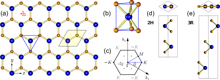
The electronic structures of 2D TMDs are largely determined by their crystal structures. Bulk TMDs have been studied decades ago ,85, 86, 87, 88, 89, 90, 91, 92, 93, 94, 95 which are known to crystallize in three different layered structures, i.e. 1T, 2H (cf. Fig. 1d) and 3R (cf. Fig. 1e). 1T is not as stable as the 2H and 3R phases for the four group-VIB TMDs we are focusing on.96 For the 2H and 3R phases, the monolayer has the identical structure and the difference lies in the stacking order of the monolayers in the layered structures. The monolayer as the elementary building block in fact consists of three atomic planes. The top and bottom planes are chalcogen atoms in a triangular lattice structure, and the middle plane is another triangular lattice of metal atoms, in trigonal prismatic coordination (cf. Fig. 1b). The three atomic layers together form a 2D hexagonal lattice, with the A-sublattice being the metal atom per site and B-sublattice being the two chalcogen atoms per site. The 2H phase of the bulk crystal has the hexagonal symmetry, having two monolayers per repeat unit, where the neighboring monolayers are 180∘ rotation of each other, with the A site of one layer right on top of the B site of the other, and vice versa (cf. Fig. 1d). The 3R phase has the rhombohedral symmetry, having three layers per repeat unit, where the neighboring layers are translation of each other (cf. Fig. 1e). First-principles calculations show that bilayer in 2H stacking is more stable than the 3R stacking.97 Thin film TMDs exfoliated from the natural crystals are mostly 2H stacking in the existing studies, even though 3R stacking is possible, albeit not frequent.97, 98
Apart from MS2 and MSe2, bulk MoTe2 can also exist in 2H phase (known as -MoTe2) below 815∘C, while at temperature higher than 900∘C it exists as metallic -MoTe2 with monoclinic structure.99, 10 -MoTe2 monolayer has been experimentally realized.3 Bulk WTe2 exists stably as metallic Td-WTe2 with octahedral coordination, but not in 2H phase.7, 8 2D form of 2H-WTe2 might exist on some substrate, but has not been realized. Most properties of the 2D MS2 and MSe2 to be discussed applies to 2D 2H-MoTe2 and 2H-WTe2, except that the two ditellurides have smaller band gap and larger spin-orbit effect than the corresponding disulfides and diselenides.100
When group-VIB TMDs are thinned down to monolayer, a critical change is the crossover from indirect band gap in bulk to direct band gap in monolayer form. Density functional theory (DFT) calculations have first pointed to a direct band gap in monolayer WSe2 101 and MoS2,102, 5 located at the corners of the hexagonal BZ, i.e. the points. WS2 monolayer was also studied a decade ago by both angle-resolved photoemission spectroscopy (ARPES) experiment and DFT calculation, which identified its valence band maximum at the points but did not draw a conclusion of direct band gap.103, 104, 105 The first experimental evidence of the direct band gap is from the PL measurements, where monolayers exhibit orders of magnitude increase in the quantum efficiency of luminescence compared to the bulk and multilayers.11, 12
Another critical difference between bulk crystals and monolayer is the symmetry. The 2H bulk is inversion symmetric, as shown in Fig. 1d. However, when thinned down to monolayer, the unit cell becomes half of its bulk counterpart, and inversion symmetry is broken. The crystal symmetry reduces from the space group for the 2H bulk to the group for a monolayer. The presence of inversion symmetry in the bulk and films with even number of layers and the absence of inversion symmetry in films with odd number of layers can be best illustrated by a spatial contrast image of second harmonic generation from a flake with thickness variations.107
In the layered structures, the van der Waals coupling between neighboring monolayers is much weaker compared to the covalent bonds that form the monolayer. Below, we will focus first on the monolayers which are of most current interest because of their direct band gap. Then we will focus on the bilayers and discuss how the interlayer coupling can affect the electronic structures. These together will form the basis to understand the electronic structures of the multilayer thin films as well as complex van der Waals heterostructures.
2.1 Monolayers
| state | majority of orbitals | minority of orbitals |
|---|---|---|
| M- | X- | |
| M- | X- | |
| M- | M-, X- | |
| M- | X- |
Critical points and orbital compositions of energy bands. – Critical points refer to the extrema or saddle points of the energy bands. They give rise to van Hove singularities in the electronic density of states, and play crucial roles in determining the transport and optical phenomena. We consider here the active bands only, i.e. the top valence band (VB) and the lowest conduction band (CB). In monolayers, the conduction band minimum (CBM) and the valence band maximum (VBM) are both located at the corners of the first BZ. The six corners belong to two inequivalent groups denoted by and points respectively, where each group has three equivalent corners related by reciprocal lattice vectors (cf. Fig. 1c). The energetically degenerate but inequivalent band extrema at and constitute a discrete index of carriers, known as the valley index or pseudospin. Low-energy electrons and holes therefore have this extra valley degree of freedom in addition to spin. and transform into each other under the time reversal operation. Hereafter we use and to denote the CBM and VBM at the points respectively. The calculated effective masses at and are on the order of ( is the free electron mass) while actual values differ between calculations depending on the lattice constants and approximation used.108, 109, 110, 111
The CB also has six local minima at the low symmetry points (cf. Fig. 1c and 2a, also referred as points in some literatures112, 113), while the VB has a local maximum at the point, which are referred to as and respectively hereafter. These critical points are also important because they are energetically close to and respectively, and in cases such as under strain or in multilayers, may become the global CBM or the global VBM. and are high symmetry points invariant under the operation (the rotation by 2 around the axis). With this discrete rotational symmetry, the dispersions in the neighborhood of these critical points are anisotropic with the three-fold rotational symmetry (i.e. trigonal warping). Interestingly, the trigonal warping, while not large, may lead to a new possibility of generating valley and spin currents that are second order to the electric bias or temperature gradient. 56 The six valleys can be divided into two groups: and . The operation transforms the three (or ) valleys into each other, while and are related by time reversal operation.
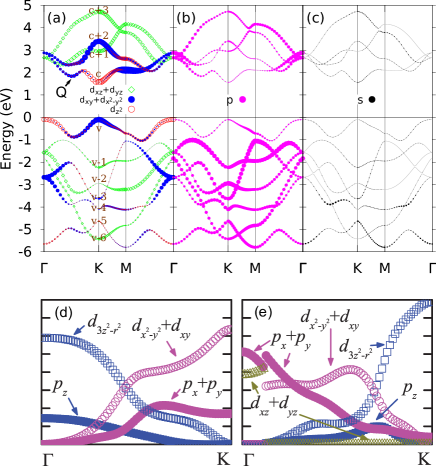
First-principles calculations find that, in monolayers, the 4 bands above the band gap and the 7 bands below the band gap are predominantly from the M- orbitals and X- orbitals. Other orbitals such as M- and X- have negligible contribution. There is perfect agreement between the first-principles bands and the Wannier bands constructed using only M- and X- orbitals.114, 115 Orbital compositions of the bulk bands of TMDs are similar to those of monolayers.90, 94 Fig. 2a-c shows the orbital compositions of MoS2 monolayer and Fig. 2d-e shows those of the WSe2 monolayer.
For monolayers, the first-principles calculations also find that the band-edge states at and are predominantly from the M- orbitals, with some mixture of X- orbitals (cf. Tab.1).101, 5, 106, 116, 117, 118, 100 For wavefunctions at and , the contributions from the X- orbitals become significant. In fact, the X- composition at and play an important role in the crossover from the direct to indirect band gap from monolayer to bulk, because the close distance between X- orbitals from neighbouring layers leads to large hopping, which changes the energy of and substantially.102, 118
Eventhough first-principles calculations have provided valuable insight into the electronic structures of TMD monolayers, we emphasize that caution should be applied when interpreting the obtained results, e.g. the band-edge locations, especially when no experimental data are available. First-principles calculations have found that the energy separations between and and between and depend sensitively on the lattice constant. It’s well known that GGA (LDA) exchange-correlation functional overestimates (underestimates) lattice constant in the energy minimization process of first-principles calculations. Hence the lattice constant determined by GGA (LDA) will introduce artificial tensile (compressive) strain, which may sometimes give conflicting results. For example, GGA calculations without SOC for MoS2 monolayer give an indirect gap with higher than by 4 meV, with the GGA lattice constant of 3.19 Å compared to the bulk experimental value 3.16 Å.100, 109 Similarly, LDA gives indirect band gap for MoSe2 and WSe2 with lower than . 100, 119, 117 In addition to lattice constant, there are other details to affect the calculated monolayer band structure, such as the GW (quasiparticle self-energy correction) method,120, 121, 122 hybrid functional, pseudopotential, and SOC. Turning on SOC, even in GGA case, will correct MoS2 monolayer from indirect to direct gap. Some GW calculations show that MoS2 monolayer has indirect gap with CBM at ,109, 123 while others give direct gap.39, 124 The inclusion of the (for Mo) and (for W) semi-core electrons is found crucial to obtain the direct gap.124
| (in ) | Mo- | S- | ||||
| c+3 | 1 | |||||
| c+2 | 1 | |||||
| c+1 | 1 | |||||
| c | 1 | |||||
| v | 1 | |||||
| v1 | 1 | |||||
| v2 | – | 1 | ||||
| v3 | 1 | |||||
| v4 | 1 | |||||
| v5 | 1 | |||||
| v6 | 1 |
Symmetry of band-edge wavefunctions. – At the points, the wave-vector group is whose generators are and (the mirror reflection about the plane across the M atoms). is an Abelian group and has only one-dimensional irreducible representations. This makes all the Bloch states at nondegenerate, which have to be eigenstate of both and . The symmetry divides the five M- orbitals into two sets: the even set } and the odd set . X- orbitals above and below the M-atom plane can also be arranged in terms of linear superpositions with odd and even symmetry respectively. When SOC is not considered, orbitals in the even set can not couple with those in the odd set. To be eigenstate of , orbitals have to combine chirally in spherical harmonic form, i.e. , , , , and . Under rotation about the atomic center of each orbital, these orbitals transform as
| (1) |
It should be noted that action of on the Bloch states includes rotations of both the constructing atomic orbitals and the plane wave component in the Bloch functions.22, 25, 73 In Tab. 2, we list the main orbital compositions and the eigenvalues of both and for all the Bloch states at the point. The corresponding eigenvalues and orbital compositions at the point are simply the complex conjugate since and are time reversal of each other. We emphasize that the eigenvalue, , of rotation depends on the position of the rotation center, , which can be M, X, or the h position (the hollow center of the hexagon formed by M and X, cf. Fig. 1a).73 M is used in the symmetry analysis of ref. 100, while h is used in ref. 25 and 125. The dependence of eigenvalues of the Bloch states on the choice of rotation center can have important consequences, for example, it gives rise to sensitive dependence of intervalley coupling strength on the central position of a lateral confinement potential that also has the symmetry.73
Valley optical selection rule. – One of the most interesting properties of the TMD monolayers is the valley dependent circularly polarized selection rules for the optical direct band gap transitions at the points.22, 23 This simply follows from the eigenvalues of the Bloch states at the points. We can establish the following identity for the interband optical transition matrix element:
| (2) | |||||
and are the Bloch states at with , , where and are integers (c.f. Tab. 2). is the momentum operator, and . The quantity characterizes the oscillator strength of the interband transition with light of circular polarization. A nonzero requires , i.e. ( modulo 3) . This is the azimuthal selection rule for allowed interband optical transitions. We note that the values of and in Eq. (2) depend on the choice of rotation center, but the value ( modulo 3) does not (c.f. Tab. 2). The selection rule between the lowest conduction and top valence bands is of particular interest. According to Tab. 2, the direct band gap optical transition is allowed at () by the () polarized light only (cf. Fig. 3e). Under time reversal operation, is transformed to , and is transformed to , so this selection rule does respect the time reversal symmetry. Inversion operation also transforms to , but it leaves the light circular polarization unchanged. Thus the valley dependent selection rule conflicts with inversion symmetry, the broken of this symmetry is the necessary condition for having such selection rule.22, 23 While the above analysis is applicable to the high symmetry points only, first-principles calculations have shown that the selection rule in fact holds approximately true in a large neighbourhood of points.25
The valley optical selection rule makes possible optical pumping and detection of valley polarization. Circularly polarized light can selectively inject photocarriers into one of the valleys, while valley polarization of electron-hole pairs will manifest as circularly polarized luminescence upon the electron-hole recombination. Initial experimental evidences of the valley optical selection rule come from the polarization resolved PL measurement where the light emission is found to have the same circular polarization as that of the excitation laser.24, 25, 26 Another unique consequence of the valley optical selection rule is the possibility to optical generate valley coherence.27 Since linearly polarized photon is the coherent superposition of and polarized photon, excitation by linearly polarized laser can optically inject electron-hole pair in linear superposition at and .
Electronic and optical band gaps and excitonic effect. – The band gap generally refers to the energy difference between the CBM and VBM, which can be determined either by transport or optical measurements. However, the size of the band gap determined from the two types of measurement differs because of the excitonic effect that is present in the optical process. The band gap determined from the transport measurement is also known as electronic band gap. It characterizes single-particle excitations and is defined as the sum of the energies needed to separately tunnel an electron and a hole into the system.46 In optical measurement, the absorption of a photon simultaneously creates an electron in the CB and a hole in the VB, which will bind through Coulomb interaction into an exciton. The energy required to creates an exciton is then referred as the optical band gap. Clearly, the difference between the electronic and optical band gaps corresponds to the binding energy of the exciton, which reflects the strength of the Coulomb interaction.
| gap | ||
|---|---|---|
| MoS2 | 1.8311, 1.9012, | |
| WS2 | 107 | |
| MoSe2 | 1.6637 | |
| WSe2 | 107 |
Optical band gaps of monolayer TMDs have been determined from PL measurements, as listed in Tab. 3. For all four group-VIB TMDs the band gaps fall into the visible frequency range, making them ideal systems to explore semiconductor optics and optoelectronic applications. The substrate and dielectric environment can change the value of the optical band gap by a few percent.12, 11, 126, 127, 128, 129, 130, 131 In high quality MoSe2 and WSe2 samples, the neutral and charged excitons are found with narrow PL linewidth of a few meV, while the separation between the neutral and charged excitons is 20-30 meV.37, 27 This makes possible a reliable characterization of the temperature dependence of optical gap, which can be well fitted by the standard semiconductor band gap dependence.37
Electronic band gap has also been measured using scanning tunneling spectroscopy (STS) and ARPES. For monolayer MoS2 on highly ordered pyrolytic graphite (HOPG), STS measurements give an electronic band gap of 2.15 eV or 2.35 eV at 77 K depending on the choice of threshold value of tunneling current,45, 132 while PL measurement on the same sample gives an optical gap of 1.93 eV at 79 K. For WSe2 and WS2 monolayers on HOPG, the STS measurement shows an electronic band gap of 2.51 eV and 2.59 eV respectively at 77 K.132 For monolayer MoSe2 grown by molecular beam epitaxy (MBE) on bilayer graphene, the STS-determined electronic band gap is 2.18 eV at 5 K, while PL shows the optical gap of 1.63 eV at 77 K.46 MoSe2 grown by MBE on HOPG substrate shows a similar electronic band gap of 2.1 eV in the STS measurement.19 In the interpretation of the STS measured gap, a possible complication is that and have much larger weight in the scanning tunneling spectra than and ,46 due to the larger density of states as well as larger tunneling coefficient at and . The latter is due to the fact that the wavefunctions at and have nonnegligible component from X- orbitals, which are closer to the STM tip. This may obscure the attribution of the band edge. ARPES measurement on heavily doped MBE grown MoSe2 monolayer has reported a much smaller band gap of eV,18 implying a large band gap renormalization due to the screening effect by the carriers.46
The difference between the measured electronic and optical band gaps point to a large exciton binding energy of hundreds of meV in monolayer TMDs. An exciton binding energy in the range of 0.3–0.7 eV has also been inferred in monolayer WX2 from spectral features in two-photon absorption and reflectance measurement which are attributed as excitonic excited states.42, 43, 41, 40 Moreover, the charging energy, i.e. energy difference between the neutral exciton and charged exciton in the PL, is measured to be in the range of 20–40 meV,37, 27, 36 which is consistent with the above binding energy for 2D excitons. These all point to exceptionally strong Coulomb interaction, due to the large effective masses of both electrons and holes and the reduced screening in the 2D limit.39, 46
There have been remarkable efforts in first-principles calculations of band gaps and the excitonic effects in monolayer TMDs.133, 108, 38, 134, 109, 135, 39, 123 DFT calculations underestimate the electronic band gap significantly. The GW method beyond DFT and based on many-body perturbation theory is generally used to obtain the electronic band gap. To calculate the exciton binding energy, Bethe-Salpeter equation (BSE)136, 137 is solved based on the GW method to obtain the optical absorption spectra and then the exciton binding energy is obtained by subtracting the optical transition energy from the electronic band gap. The exciton binding energy from these calculations agrees in order of magnitude with the experiments. For monolayer MoSe2, the experiments and first-principles calculations agree quantitatively well on the electronic band gap and the exciton binding energy.46 However, the obtained exciton binding energy depends on the computational details. sampling not dense enough overestimates the exciton binding energy,109, 138, 123 while finite interlayer separation underestimates the exciton binding energy.134, 123 The underestimation from finite interlayer separation can be solved by using extrapolation as the interlayer separation going infinite134 or by using truncated Coulomb interaction,39, 123 and the latter method is considered more reliable.123 In addition, including the electron-phonon interaction will result in red shift of the absorption peak obtained in BSE and affect the exciton binding energy consequently.139 A rather interesting observation from these first-principles calculations is that the GW correction and the exciton binding energy have comparable value, giving rise to the accidental agreement between the DFT calculated gap and the measured optical gap.109, 39
The exciton Bohr radius calculated with the GW-BSE method is on the order of 1 nm,38, 39, 135 still a few times larger than the lattice constant. So the exciton in monolayer TMDs is of mixed character: the binding energy is comparable to typical Frenkel excitons, while the wavefunction of the electron-hole relative motion is largely of the Wannier type, extending over a large number of unit cells. Correspondingly, the exciton wavefunction is well localized in momentum space. A bright exciton that can emit photon has its electron and hole constituents both localized in the or valleys. These valley excitons well inherit the valley optical selection rule of the band-to-band transition. Namely, the () valley exciton can be interconverted with () photon. This selection rule forms the basis of the recently demonstrated optical generation of excitonic valley pseudospin polarization and coherence.26, 24, 25, 27 The strong Coulomb interaction in monolayer TMDs also gives rise to pronounced exchange interaction between the electron and hole constituents of the exciton, which strongly couples the valley pseudospin of exciton to its center of mass motion.140
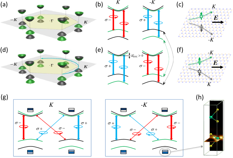
Spin-orbital interaction and spin-valley locking. – TMDs have a strong SOC originated from the orbitals of the metal atoms. The form of SOC induced spin splitting of bands in monolayers can be fully determined by symmetry analysis. The first constraint is from , the mirror reflection symmetry about the metal atom plane, which dictates a Bloch state and its mirror reflection to have identical energy. The mirror reflection of an in-plane spin vector is its opposite, while the mirror reflection of an out-of-plane spin vector is itself. Thus spin splitting is allowed in out-of-plane () direction only, where the spin expectation value of the Bloch states is either along the or direction. Secondly, the time reversal symmetry dictates the spin splittings at an arbitrary pair of momentum space points and to have identical magnitude but opposite sign.34 In the neighborhood of and , the SOC then manifests as an effective coupling between the spin and valley pseudospin, i.e. with the sign of the spin splitting conditioned on the valley pseudospin. We note that inversion symmetry would impose a conflicting constraint from that of the time reversal symmetry, so inversion symmetry breaking in the monolayer is the necessary condition for having this spin-valley coupling.
| (eV) | (eV) | ||||
|---|---|---|---|---|---|
| GGA | HSE108 | GW108 | GGA100 | ||
| MoS2 | 0.148,106, 100 0.146108 | 0.193 | 0.164 | 0.003 | |
| WS2 | 0.430,100 0.426,106, 0.425108 | 0.521 | 0.456 | 0.029 | |
| MoSe2 | 0.184,100 0.183106, 108 | 0.261 | 0.212 | 0.021 | |
| WSe2 | 0.466,100 0.456,106 0.461108 | 0.586 | 0.501 | 0.036 | |
First-principles calculations with GGA find that the VB at point has a SOC of eV for the MoX2 monolayer and eV for WX2 monolayer, while the HSE hybrid functional and GW calculations give slightly larger values (cf. Tab. 4).106, 23, 108 Experimental evidence for such a giant SOC is reflected in PL measurements where two peaks, attributed as excitons with the holes from the two split-off spin subbands respectively, are seen with an energy separation in agreement with the VB spin splitting at .12, 107 Lately, the ARPES measurement of MBE grown MoSe2 gives a direct evidence of the VBM SOC splitting of 0.18 eV,18 in agreement with the calculations. Because of this giant SOC, the VBM in monolayer TMDs has the spin index locked with the valley index, i.e. valley () has only the spin up (down) holes (cf. Fig. 3a). Another important consequence of the SOC is the valley dependent optical selection rule becomes a spin dependent one as well.23 For example, polarized light still excites only the valley, but depending on the light frequency, it can either resonantly excite spin up or down carriers (cf. Fig. 3e).
The CB at also has the spin splitting with the same symmetry-dictated form as the VB. The magnitude, however, is much smaller, about a few meV for MoS2 and tens of meV for other TMDs from first-principles calculations (cf. Tab. 4), 133, 141, 116, 125, 142, 143, 144, 100, 115, 72 and some experimental evidences of this SOC splitting has been reported recently.145 The small CB SOC is due to the fact that the CB Bloch states at are predominantly formed by the M- orbitals where the intra-atomic coupling as the dominant contribution to SOC vanishes to the leading order. Interestingly, the first-principles calculation finds an overall sign difference of the CB splitting between MoX2 and WX2.100 The CB splitting originates from the first order effect from the small X- compositions, as well as the second-order coupling mediated by the remote conduction bands consisting of M- orbitals (cf. Tab. 2).144, 125, 100 The two contributions to SOC have opposite sign and their competition leads to the sign difference between MoX2 and WX2.100, 115
For the valleys of the CB, sizable spin splittings are also found in the first-principles calculations.56 The three () valleys have the same spin splitting as they are related by the rotation, while the splittings at and have opposite sign. In the neighborhood of , the spin splitting has a quadratic dependence on the wavevector with a three-fold pattern for the sign. 56
Berry phase related properties. – The Berry phase effect for a particle lies in the dependence of the internal structure on the dynamical parameter. In the context of Bloch electrons, it is the dependence of the periodic part of the Bloch function on the wavevector .146 The Berry curvature and orbital magnetic moment are two physical quantities that characterize the effect of Berry phase of electrons in the Bloch bands. The Berry curvature is defined as: . In an applied electric field, the Berry curvature gives rise to an anomalous velocity , i.e. a Hall effect (cf. Fig. 3c, f). Thus, Berry curvature plays the role of a magnetic field in the momentum space. For 2D crystal, Berry curvature is a pseudo-vector in the out-of-plane () direction, and its projection along the axis is:
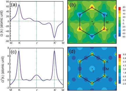
where is the velocity operator and is the energy dispersion. In monolayer TMDs, sizable Berry curvature is found in the neighborhood of the points from theoretical modeling and first-principles calculations.23, 21, 25, 114 As the and valleys are time reversal of each other, the Berry curvature must have opposite values at and (cf. Fig. 4a-b). The Berry curvature is invariant under spatial inversion that also transform and into each other. Thus, inversion symmetry breaking is the necessary condition for having the valley contrasting Berry curvature.
By the valley contrasting Berry curvature, an in-plane electric field can drive the carriers at the and valleys to the opposite transverse edges (cf. Fig. 3c, f). Such a valley dependent Hall effect is an analog of the spin Hall effect, but with valley pseudospin playing the role of spin. Valley Hall effect in monolayer MoS2 transistor has been reported recently in experiments.29 For hole doped systems, because the spin is locked with the valley index at the VBM, the valley Hall effect is also accompanied by a spin Hall effect with the same Hall conductivity (up to a proportionality constant). For electron doped case, the spin up and down electrons in the same valley have slightly different Berry curvature (cf. Tab. 6), which also gives rise to finite, albeit smaller, spin Hall effect.23, 114 This is illustrated in Fig. 4c-d, which shows the first-principles calculated spin Berry curvature
being the spin current operator defined as . At the CBM and VBM where spin up and down states are not mixed, the spin Berry curvature is simply given by . Fig. 4c-d also shows finite spin Berry curvature near where spin Hall effect is also expected.
Berry curvature is in general accompanied by the orbital magnetic moment, which can be viewed as the self-rotating motion of the electron wavepacket.146 Similar to the spin magnetic moment, the orbital magnetic moment will lead to Zeeman shift in a magnetic field. The time reversal symmetry also requires the orbital magnetic moment to have identical magnitude but opposite signs at and . Therefore, similar to the spin, the two valley pseudospin states are associated with opposite magnetic moment, making possible magneto-control of the pseudospin dynamics.30, 32, 31 The valley contrasting Berry curvature and magnetic moment, as well as the valley and spin dependent optical selection rules, make TMD monolayers ideal platform for investigating spintronics and valleytronics.
Strain effects on band structures. – Strain can tune various physical properties in monolayer TMDs including the band gap, band edge locations, effective mass, phonon mode, and magnetism, as shown in theoretical 66, 147, 148, 149, 150, 151, 38, 152, 109, 119, 117, 153, 154, 155, 156, 157 and experimental studies. 129, 152, 158, 159, 160 First-principles calculations show that biaxial tensile strain in MoS2 monolayer lifts the energies of and points, and under moderate strain () the band gap can cross from the direct one () to an indirect one () 151, 148, 109, 147. The calculations also find that the band gap decreases with the biaxial tensile strain and the monolayer may become a metal under larger strain of 8–10.151, 148, 149 In contrast, calculations find that biaxial compressive strain in MoS2 monolayer lowers the energies of and points, and the band gap also crosses to an indirect one (, different from the tensile case). Meanwhile, the band gap increases with compressive strain up to a strain strength 147, 66, 117 and then decreases with larger strain until becoming metallic.151 Other TMD monolayers have qualitatively the same behaviors under biaxial strain.149, 147, 119, 117 Uniaxial strain on TMD monolayers are also studied using first-principles calculations, where similar but quantitatively smaller effects are found.149, 117 Experiments show that uniaxial tensile strain results in red shift of both PL and Raman peaks,159, 158, 129 consistent with first-principles calculations.
Interesting strain effects on valley pseudospin properties in monolayer TMDs have also been predicted. Uniaxial tensile strain breaks the symmetry and results in an in-plane Zeeman field on the valley pseudospin of excitons.140 A moderate strain () can lead to a sizable valley pseudospin splitting of a few meV at zero exciton center-of-mass momentum. It has also been predicted that inhomogeneous shear strain may lead to valley-contrasting effective magnetic field in the out-of-plane direction for carriers, and spin polarized Landau levels can develop.161, 162, 163, 164 These all point to interesting possibilities towards mechanical control of spin and valley pseudospin of excitons and carriers.
2.2 Bilayers and heterostructures
First-principles calculations find that 2H stacking is the most stable configuration for homostructure bilayer TMDs.165, 166, 167 In the 2H stacking, the upper layer is the 180∘ rotation of the lower one, which is an operation that switches the two valleys (cf. Fig. 3a-f). Thus the valley dependent physical properties of each monolayer, including the valley optical circular dichroism and valley Hall effect, would average to zero in the pristine 2H bilayer (cf. Fig. 3), as required by the restoration of inversion symmetry (cf. Fig. 1d). Nevertheless, a perpendicular electric field can break the inversion symmetry, and leads to the emergence of valley circular dichroism and valley Hall effect.22, 28, 33 This makes possible a controllable way to tune the valley physical properties by changing the symmetry of the system. Preliminary evidence for such tunability has been reported in bilayer MoS2 where the PL circular polarization as a signature of the valley circular dichroism can be switched on and off by the interlayer bias.33 The PL circular polarization has also been used to indicate the inversion symmetry breaking in the MoS2 bilayer.97, 98 Non-zero PL circular polarization is generally observed in as-prepared 2H MoS2 bilayer in the absence of external gating, implying the existence of perpendicular electric field from the substrate effect, consistent with the presence of large n-doping.33, 26
| bilayer | band edge | refs |
|---|---|---|
| MoS2 | 11, 168, 169, 170, 171, 34, 113, 142, 167 | |
| 172, 151, 170, 147, 166, 165, 66, 133, 112, 173 | ||
| WS2 | 170, 147, 171, 112, 107, 113, 142, 167, 34 | |
| 168 | ||
| 34 | ||
| MoSe2 | 170, 171, 138, 113, 167, 34 | |
| 147 | ||
| 34 | ||
| WSe2 | 101, 147, 107, 113, 34, 167 | |
| 171 | ||
| 112 |
Band edges. – The first-principles calculated band structures of TMD bilayers, in particular the band edges and band gaps, depend on the parameters and approximations used (cf. Tab. 5). Lattice constant and interlayer distance are the two geometry parameters affecting the band edges most. DFT without the van der Waals correction will overestimate the interlayer distance in the GGA calculations170, 165 (may also underestimate a little in LDA166, 171), resulting in too small interlayer interactions to describe the bilayers reasonably. First-principles calculations of bilayer MoS2 with geometry parameters using measured bulk values and the van der Waals relaxation results (PBE-D2174) lead to different indirect band gaps of and respectively 170. For WS2 and MoSe2 bilayers, larger interlayer distance, i.e. the van der Waals relaxed one compared to the bulk one, will change the VBM from to .34 Other computational details such as the SOC, exchange correlation functional, pseudopotential, and GW may also give different results, e.g. including SOC can change the VBM of WSe2 bilayer from to .107, 113 The only direct evidences available are the ARPES studies which show the VBM at for MoS2 and MoSe2 bilayers175, 18. More experimental studies are needed for determining the band edges and band gaps in bilayer TMDs under various conditions.
The sensitive band-edge dependence on the lattice constant and interlayer distance points to significant strain effects. MoS2 bilayer under in-plane biaxial strain are found to behave similarly to its monolayer counterpart: (i) band gap decreases with the increase of tensile strain; (ii) under compressive strain the gap first increases and then decreases; (iii) under large enough strain of either tension or compression, the bilayer can become metallic.151, 66 Under out-of-plane compressive strain, TMD bilayers can also undergo semiconductor-to-metal transition.165 In addition to strain, perpendicular electric field can also decrease the band gap of TMD bilayers near linearly.170, 166, 176
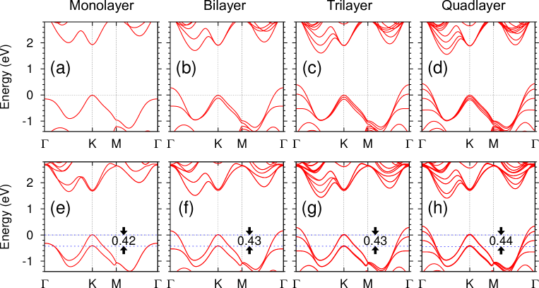
Interlayer hopping. – The crossover from direct band gap at monolayer to indirect band gap at bilayer and multilayers is a consequence of interlayer hopping. It can be seen from Fig. 5a-d that the band extrema , and all split with the increase of the number of layers, a direct evidence of the interlayer hopping. The splitting represents the interlayer hopping strength. The splitting at and are much larger than that at . This is due to the fact that the Bloch states at are predominantly from the metal orbitals, while the Bloch states at and have non-negligible compositions of the chalcogen orbitals (cf. Fig. 2). The interlayer hopping integral between the orbitals of the nearest neighbor chalcogen atoms is more significant compared to other orbitals. The interlayer hopping at is then much weaker compared to that at and , because the two metal planes have larger separation compared to the two nearest neighbor chalcogen planes from the two layers. With the increase of the number of layers, the energy of is raised and that of is lowered significantly, while the energies of and do not change much. The band gap crosses over to an indirect one at bilayer, and further decreases with the increase of thickness.
Right at , there is no visible splitting from the interlayer hopping (Fig. 5 a-d). This is dictated by the rotational symmetry of the 2H bilayer lattice and the Bloch functions of each monolayer. The interlayer hopping matrix element is , where () is the Bloch state at point in the lower (upper) layer. is the interlayer hopping between the two layers which, in 2H stacking, is invariant under rotation (i.e. ). Thus
| (3) | |||||
in which and are the eigenvalues of the rotation for and respectively. A nonzero interlayer hopping matrix element then requires . Assuming the lower layer takes the orientation in Fig. 1a, is directly given in Tab. 2, while is given by the complex conjugates of those in Tab. 2 because of the 180∘ rotation between the two layers that switches and . Take the rotation center to be the M site in the lower layer (X site in the upper layer), we have for the VBs, while and for the CBs. These mean that interlayer hopping is allowed between the VBM states, but is forbidden between the two CBM states at point in the lower and upper layers. The strength of the VB interlayer hopping can be read out from the splitting at in the absence of SOC, which is in the order of meV in all four TMDs.34 Moreover, for the Bloch states at point with c+1, v-4, or v-6 (cf. Fig. 2), the identical eigenvalues under in the upper and 180∘-rotated lower layers (, cf. Tab. 2) imply that these states have finite interlayer hoppings and hence split in 2H bilayers.
means that no interlayer hopping exists to the leading order between the states in the upper and lower layers. In fact, in the absence of SOC, states in the upper layer and lower layer belong to different irreducible representation of the symmetry, thus interlayer hopping vanishes to all orders between the states in the two layers.111We note that small yet finite (meV) interlayer splitting exists for the states calculated by the VASP software. This splitting is confirmed to be artificial due to the numerical errors introduced by VASP. TMD bilayers calculated by a more accurate software, i.e. WIEN2k, show no splitting for the state, which is consistent with the symmetry analysis. We note that this conclusion is unique to the 2H stacking order. A relative translation or rotation of the two layers will change the rotational symmetry of , allowing a finite interlayer hopping between the states.
Spin-layer locking effect in valleys. – An interesting feature in 2H (or 2H-like) stacking is the interlayer hopping at valleys can be substantially quenched by the SOC. As shown in Fig. 5e-h for WS2, with SOC turned on in the first-principles calculations, the band dispersions at become nearly identical for mono-, bi-, tri-, and quad-layers, exhibiting only a splitting of eV which is nearly the spin-orbit splitting shown in Fig. 5e. This is due to two facts: (i) in each monolayer there is an out-of-plane spin splittings with opposite signs in the and valleys; (ii) the lower layer is an 180∘ rotation of the upper one in the 2H stacking. This rotation switches the two valleys in the lower layer, but leave spin unchanged (cf. Fig. 3a,d). Thus, the sign of the spin splitting depends on both the valley index and the layer index. Since interlayer hopping conserves both the spin and the crystal momentum, the spin splitting corresponds to an energy cost of the interlayer hopping (cf. Fig. 3b,e), which is larger than the hopping matrix element.34, 35 Thus interlayer hopping is effectively quenched, especially for WX2 where SOC is stronger. In 2H bilayers, the Bloch states in the valleys are predominantly localized in either the upper or the lower layer depending on the spin, i.e. the spin index is locked with the layer index (cf. Fig. 3g-h). The valley physics is essentially that of the two decoupled monolayers. The valley circular dichroism and valley Hall effect from the two layers average out, but the spin circular dichroism and the spin Hall effect from the two layers add constructively (cf. Fig. 3c,f,g).34 Circular polarized PL can now come from the spin circular dichroism and is not necessarily an indication of inversion symmetry breaking.34, 35 Since the layer degree of freedom is associated with the out-of-plane electric polarization, while spin couples to magnetic field, the spin-layer locking also leads to a variety of interesting magnetoelectric effects.34, 33, 177
Heterostructures of different TMDs. – Manually assembled (stacked) monolayers can lead to a variety of vertical heterostructures between different group-VIB TMDs 178, 179, 180, 181, 145, 132 and between TMDs and other 2D crystals4, 182 , which are of interest because they make possible semiconductor heterojunctions in the 2D limit.
First-principles calculations have studied various lattice matching heterostructures of either the AB stacking (M/X site of one layer right on top of X/M site of the other) or the AA stacking (M/X site of one layer right on top of M/X site of the other). These heterobilayers have the same hexagonal BZ as the monolayers. Unlike TMD homobilayers which all have indirect band gaps, calculations show that some of these lattice matching heterobilayers exhibit direct band gaps at the points. For example, MoS2-WSe2 and WS2-WSe2 heterobilayers are found to be direct band gap semiconductors in the various first-principles calculations reported.183, 184, 113 MoS2-WS2 heterobilayer is reported to have indirect band gap183, 184, 113, 185 or direct band gap 141 depending on the interlayer distance adopted in the calculations. Like the homobilayers, computational details, such as van der Waals corrections, SOC, GW corrections, matched lattice constant with strain, etc, may give some different details of the band structures of the heterobilayers.186, 184, 185, 141
An interesting observation from these first-principles calculations of heterobilayers is that the CB and VB states at the points are predominantly localized in an individual layer. In particular, they exhibit the type-II band-edge alignment with the CBM and VBM residing in opposite layers.113, 141, 187, 184, 185 Such type-II heterojunctions result from the workfunction and band gap differences between the TMDs. The resultant conduction band offset (CBO) and valence band offset (VBO) between the monolayers are found to be a few hundred meV from these calculations. Note that the CBO and VBO correspond to the energy cost of interlayer hopping, hence the large CBO and VBO will substantially quench the hybridization between the layers, making the band structures of the heterobilayers almost the superposition of that of the constituent monolayers.185, 141, 132
According to the measured bulk lattice constants: 3.160 Å for MoS2,188 3.153 Å for WS2,189 3.288 Å for MoSe2,188 and 3.282 Å for WSe2,189 lattice matching heterobilayers are more likely to form between MoS2 and WS2, and between MoSe2 and WSe2. For other combinations with large mismatch in the lattice constants, first-principles calculations have found that the interlayer couplings (van der Waals interactions) are not strong enough to make the two layers match their lattices.187. The manually assembled TMD heterostructures in general leads to misalignment between the layers.
For the manually stacked TMD bilayer heterostructures, optical studies have shown the spectral features of both the intralayer exciton with electron and hole from the same layer and the interlayer exciton with electron and hole from the different layers.178, 179, 180, 181, 145 For example, in the MoSe2-WSe2 heterostructures,145 neutral and charged intralayer excitons from both the MoSe2 layer and WSe2 layer can be clearly identified in the PL spectral from the heterojunction region, and they have identical energies to the ones in isolated MoSe2 monolayer and WSe2 monolayer. These further confirm that hybridization between the layers is small for the band edge states. The interlayer exciton is found to have an energy a few hundred meV below the intralayer one, consistent with the type-II band edge alignment and the magnitude of CBO and VBO from the first-principles calculations.
For MoS2-WS2 and MoS2-WSe2 heterostructures, the VBO and CBO have also been directly measured by micro-beam X-ray photoelectron spectroscopy (XPS) and STS.132 For MoS2-WSe2 heterostructure, the VBO is directly measured to be 0.41 eV by the XPS. This VBO can also be inferred from STS measurements of monolayer MoS2 and WSe2 both on graphite, where the deduced VBO is 0.36 eV, consistent with XPS result. And the deduced value for CBO between MoS2-WSe2 is 0.52 eV from STS and 0.57 eV combining the VBO from XPS and the band gap measured from STS. The CBM is found to reside in the MoS2 layer and VBM in the WSe2 layer. MoS2-WS2 heterostructure is shown to be a similar type-II heterojunction with a smaller VBO of 0.23 eV measured using XPS, and a deduced CBO of eV. WS2-WSe2 heterostructure is also shown to be a type-II heterojunction with CBM in the WS2 layer and VBM in the WSe2 layer, while both CBO and VBO are eV.132
In these type-II heterostructures, the observation of interlayer exciton in the PL spectrum show that there is residue hybridization between the layers, such that CBM electrons still have a finite albeit small spatial overlap with the VBM holes residing largely in the opposite layer. The interlayer exciton is therefore still optically bright, but has much smaller optical dipole compared to the intralayer exciton. This gives rise to long recombination lifetime measured for interlayer exciton which exceeds ns,145 orders of magnitude longer than the intralayer ones. With electron and hole constitutions in opposite layers, interlayer exciton correspond to permanent electric dipole in the out-of-plane direction, evidenced from the gate dependence of its resonance energy. 145 Repulsive interactions between these dipole-aligned interlayer excitons are also inferred from the excitation power dependence of the PL spectra. With the observed ultralong lifetime and the repulsive interaction,145 the interlayer exciton in TMD heterostructures may provide an ideal system to explore the exotic phenomenon of excitonic condensation,190 as well as optoelectronic applications such as the excitonic circuit and heterostructure lasers. Such interlayer excitons will also form the basis for optical control of layer degree of freedom in van der Waals layered structures.
3 Theoretical models
Theoretical models have been developed at different levels to describe the complex electronic structures of TMD monolayers, including both models23, 191, 125, 100 and TB models.191, 173, 118, 100, 142 Among the various models, the simplest and widely used one is the two-band model describing the neighborhood of the points 23
| (4) | |||||
in which is the Pauli matrix spanning the conduction and valence states at points, which are formed respectively by the and orbitals respectively. is the valley index, and is the spin index. is the lattice constant, and is the wave vector measured from . The effective hopping integral , the band gap , and the SOC splitting in the VB can all be fitted from the first-principles band structures in the neighborhood of points. Interestingly, this two-band model is in fact the massive Dirac fermion model. This simple model explains why the electron and hole masses are comparable, since they are largely acquired from the mutual coupling of the two bands. It also well captures the low-energy band-edge physics in the valleys, including the band dispersion, the giant SOC splitting of the VB, the valley dependent Berry curvature and orbital magnetic moment, and the valley dependent optical selection rule.23 Table 6 is a comparison of the Berry curvatures from this model and from first-principles calculations for the four monolayer TMDs, which shows remarkable agreement.
| MoS2 | MoSe2 | WS2 | WSe2 | |
| 38.8 | 39.7 | 59.8 | 64.3 | |
| 35.3 | 36.5 | 55.4 | 60.0 | |
| 31.6 | 30.0 | 34.9 | 34.7 | |
| 29.5 | 28.4 | 34.2 | 33.3 | |
The SOC in this two-band model is from the intra-atomic contribution , thus it vanishes for the CB, missing the two origins of the small CB splitting: the second-order coupling with remote M- orbitals; and the first-order effect from the minor X- compositions.144, 125, 100, 115 Nevertheless, the CB spin splitting has to take the same symmetry-dictated form as the VB one as discussed earlier.35 This valley dependent spin splitting term can be phenomenologically added to the CB edge for correction.192, 72, 144
The two-band model has been widely used to study various properties of TMD monolayers because of its simplicity.193, 194, 195, 196, 135, 197, 198, 199, 192, 200, 201, 202, 203, 204, 205, 206 In the meantime, the simplicity of this model inevitably imposes some limitations on its applications. For example, it can not account for the electron-hole asymmetry and the trigonal warping of band dispersion. The two limitations can be overcome by introducing terms quadratic in 191, 100 or cubic in .125, 100 The corrected models with high-order terms have been used to study optical conductivity,207 magneto-optical properties,192 plasmons,208 and spin relaxation.209 Apart from the most studied valley, the valley of VB can be well described by an effective-mass model nearly unaffected by SOC.125 For the valleys of CB, there lacks simple models because of its low symmetry.
While the approximation aims to describe the electronic structures only in the neighborhood of a critical point of high symmetry in the momentum space, TB models can in principle reproduce the band dispersions in the entire BZ, suitable for studying edge states, finite size systems such as quantum dots, as well as for calculating mesoscopic transport. TB models have been constructed for TMD monolayers in various approximation levels, with different number of bands (or the number of orbitals in a unit cell) involved and different cut-off distances of hoppings. There are (i) 7-band and 5-band TB models,191 (ii) 27-band TB model,173 (iii) 11-band TB model,118, 142 and (iv) 3-band TB model.100 Here the number of bands is counted in the spinless case, and the actual number of bands doubles when SOC is added to the model.
(i) The 7-band TB model191 contains three Mo- orbitals (Mo-), four S- orbitals (upper and lower S-), only Mo-S nearest-neighbor (NN) hoppings, and overlap integrals. The hopping integrals are in the Slater-Koster (SK) two-center approximation.210 Then the model is reduced to a 5-band model whose basis states all have even symmetry under . The model can describe the lowest CB and the top VB in the valleys, while there is large discrepancy over the rest -space region.191 Another limitation is that it does not reproduce correctly the order in energy of other conduction and valence bands. This model has been used to derive the two-band model with quadratic terms by expansion at followed by reduction to the two bands in the Löwdin partitioning method.211, 212
(ii) The 27-band TB model 173 contains the complete set of orbitals of the metal atom and the two chalcogen atoms. The model considers NN SK hoppings of M-M, M-X, and X-X as well as the corresponding overlap integrals. The total number of parameters of the model is 96. It well reproduce all bands from the first-principles bands (in energy range of eV) in the entire BZ . Moreover, this model can apply to monolayer, bulk, and bilayer using the same set of parameters, all in good agreement with the first-principles bands. This model is suitable for numerical studies in need of accurate band descriptions in the entire BZ, but can be too complicated for many studies.
(iii) The 11-band TB model 118 contains five M- orbitals and three orbitals for each of the two X atoms. This model also considers NN SK hoppings of M-M, M-X, and X-X like the 27-band model, while this model uses orthogonal bases and hence does not need overlap integrals. When SOC is not considered, the 11-band model can be divided into decoupled block and block which consist of even and odd parity states respectively under the operation. This model is relatively complete in orbitals for the generally concerned 11 bands (4 above and 7 below the band gap) and keeps its relative simplicity compared to the 27-band model. Because both the VB and CB are -even, only the parameters for the -even block are fitted.118 The fitted bands agree qualitative well with the first-principles band structures, but the quantitative discrepancy can be large away from the and points. With interlayer X-X hoppings considered, this model can be used to qualitatively explain the direct-to-indirect band gap transition from monolayer to bulk. SOC interactions have been added to the latest development of this 11-band model to make it more realistic.142
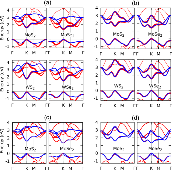
(iv) The 3-band TB model 100 is constructed with the three M- orbitals only, i.e. , , and . Symmetry-based non-SK M-M hoppings of both NN interactions and up to the third-nearest-neighbor (TNN) interactions are considered in this model. Orthogonal bases are used so that overlap integrals are not needed. Fitting parameters are given for all MX2 monolayers in this model. The bands from the NN TB model agree well with the first-principles ones only for the VB and CB in the valleys (cf. Fig. 6a, c), while the bands from the TNN TB model agree well with the first-principles ones in the entire BZ due to the introduction of more hoppings (cf. Fig. 6b, d). With the absence of X- orbitals in the model, physical quantities such as Berry curvature which rely on the wavefunction structure can be described well only in -space regions where M- orbital dominates over the X- orbitals (e.g. VB and CB in valleys) for both the NN TB and TNN TB models. The SOC splitting of VB can also be well described. Due to the simplicity of this model, it can be particularly useful in the study of many-body physics and finite size systems. This model has been applied to the study of edge states in MX2 nanoribbon,70 quantum dots formed by lateral confinement potential in extended MX2 monolayer,73 intercellular orbital magnetic moment,31 magnetoelectronic and optical properties,213 and magnetoluminescence.214
All the TB models introduced above are capable of describing the low-energy physics of monolayer TMDs in the valleys. The 3-band TNN TB model is the simplest model that gives a reasonably good description of the top VB and lowest CB in the entire BZ. In order to capture features such as the CB splitting, M- and X- orbitals have to be included, as in the 11-band and 27-band models, which complicates the models inevitably. The TB models in (i)–(iii) are all based on the SK two-center approximation, while the 3-band TB model in (iv) is not SK-like but fully based on the symmetry. SK hoppings omit all contributions from three-center integrals, while symmetry-based non-SK hoppings include three-center integrals and make no approximations. This difference can be crucial. For example, besides 2 onsite energies, the 3-band NN TB model has 6 hoppings. However, if the 3-band model is constructed in the SK approximation, there are only 3 hoppings, namely , , and . The agreement between the TB bands and first-principles bands can always be improved by having more fitting parameters, either by introducing more orbitals or by introducing more hopping integrals. The success of the 3-band model with the relative simplicity suggests that going beyond the SK framework can be a viable way of improving the accuracy of the models.
By introducing interlayer hoppings, all the TB models for monolayer can be extended to describe bilayer and multilayer homostructures. Interlayer hoppings are explicitly included in both the 27-band and the 11-band TB models to describe bilayer or bulk. In general, the X- orbital should be included in a TB model to describe the interlayer interactions reliably, since it plays a crucial role in the interlayer hopping over a large range of the BZ, e.g. at and . However, if only the physics in valleys are of interest, effective interlayer hoppings can also be included in models constructed with M- orbitals.
For 2H bilayers, a four-band model has been derived based on the 3-band TB model of monolayers,33, 34
| (5) |
in which . In this model, only the -independent leading order term is retained for the interlayer hopping matrix element. The interlayer hopping exists only between the VB states in the two layers, while it vanishes between the CB states at due to the symmetry (see discussion in section 2.2). The magnitude can be extracted from the VB splitting at from the first-principles calculations of the bilayer band structures in the absence of SOC. CB SOC and interlayer bias can be phenomenologically added to this model. This Hamiltonian has been used to describe the tunable valley optical circular dichroism and orbital magnetic moment as a function of interlayer bias,33 as well as the magnetoelectric effects in the 2H stacked bilayers.34, 35
In the very proximity of , the above bilayer Hamiltonian simply reduces to:
| (6) |
where is the Pauli matrix for the layer pseudospin: for upper layer and for lower layer. and are respectively the valley pseudospin and the real spin. 34, 35 The SOC term corresponds to the spin splitting in the out-of-plane direction with a valley and layer dependent sign in 2H bilayer, as discussed in section 2.2. It manifests as an effective coupling between the spin, valley pseudospin and the layer pseudospin in bilayer. is the interlayer hopping term that conserves the spin and the crystal momentum. The competition of the SOC term and the interlayer hopping term determines the small hybridization between the two layers in the proximity of . The energy eigenstates are associated with a spin- and valley-dependent layer polarization , which are found in excellent agreement with the first-principles wavefunctions.34 The interlayer hopping and hence layer hybridization at vanishes due to symmetry. This difference in the layer hybridization at and can result in their different energy shifts in a perpendicular electric field, which has explained the observed splitting of interlayer and intralayer trion resonances as a function of interlayer bias in the PL measurement.35
4 Conclusions
In this review article, we provide an overview of the current understanding of the various aspects of the electronic structures in 2D group-VIB TMDs and the theoretical models developed for describing the essential features. Apart from the two-dimensionality and the visible-frequency-range direct band gap at the monolayer limit, these 2D semiconductors are distinguished from all existing systems by their extraordinary properties including the valley pseudospin of band edge carriers, the valley dependent Berry phase related properties, the ultra-strong spin-orbit coupling that lead to the strong interplay between spin and various pseudospins, and the strong Coulomb interaction evidenced from the exceptionally large excitonic effects. These imply varieties of interesting opportunities for the exploration of device applications as well as fundamental new physics. Although the electronic structures are complex in general with the involvement of multiple orbitals of metal atom and orbitals of chalcogen atom, the band edge physics in valleys which is of most interest for transport and optical studies is well understood with remarkably simple model that makes a good example of massive Dirac fermions in the limit of large gap opening.
We note that this review article has a limited scope, focusing only on the single particle electronic structures of the 2D bulk. This is partially due to the lack of understanding of the many-body effects,215 and the electronic structures on the edges, grain boundaries, and impurities. Even for the 2D bulk, several aspects of the electronic structures still remain unclear and need further experimental and theoretical studies to clarify, and we mention a few here. An outstanding issue of most importance is to determine the difference between the electronic and optical band gaps, i.e. the exciton binding energy. First-principles calculations and various experimental studies using STS, ARPES, optical spectroscopies have agreed on the order of magnitude of this quantity, while quantitative agreement is yet to be achieved. The accurate experimental determination of the exciton binding energy and the exciton excited state are also essential in understanding the screened Coulomb interaction in these 2D semiconductors.39, 46 The energies of the and valleys relative to the CBM and VBM in monolayers remain unclear. These quantities can be crucial in the study of intervalley relaxation of band edge carriers which is likely to be mediated by these valleys close by in energy. The energies of and from first-principles calculations are various due to the choice of approximations and the lack of accurate information on lattice constant. The same problem has also led to the conflicting conclusions on the indirect band gap and VBM and CBM in bilayers from the first-principles calculations. ARPES and STS can provide powerful approaches to determine the energies of these valleys.18, 46, 45
A lot of recent experimental efforts have been placed on the study of heterostructures between different 2D TMDs,178, 179, 180, 181, 145, 132 which may lead to even richer possibilities for new physics and device applications. The understanding of the interlayer hopping process is indispensable in the exploration of the new properties of the heterostructures. First-principles calculations of AB and AA stacked heterostructures have suggested that the hybridization between the layers is weak, due to the large band offsets revealed from STS and XPS,132 and PL measurement.178, 179, 180, 181, 145 The order of magnitude of the hopping matrix element is of importance in determining the optical dipole moment of interlayer exciton, and its dependence on the twisting angle between the layers is of interest. First-principles calculations can only address very limited cases of the heterostructures, and efficient theoretical models are needed with input from the first-principles calculations.
Acknowledgments
WY acknowledges support by the Croucher Foundation under the Croucher Innovation Award, and the RGC (HKU17305914P, HKU9/CRF/13G) and UGC (AoE/P-04/08) of Hong Kong SAR. GBL acknowledges support by the NSFC with Grant No. 11304014, the National Basic Research Program of China 973 Program with Grant No. 2013CB934500 and the Basic Research Funds of Beijing Institute of Technology with Grant No. 20131842001 and 20121842003. DX acknowledges support by the National Science Foundation, Office of Emerging Frontiers in Research and Innovation (EFRI - 1433496). YY acknowledges support by the MOST Project of China with Grants Nos. 2014CB920903 and 2011CBA00100, the NSFC with Grant Nos. 11174337 and 11225418, the Specialized Research Fund for the Doctoral Program of Higher Education of China with Grants No. 20121101110046. XX acknowledges support by DoE, BES, Materials Science and Engineering Division (DE-SC0008145), the National Science Foundation (DMR-1150719), and the National Science Foundation, Office of Emerging Frontiers in Research and Innovation (EFRI - 1433496).
References
- Novoselov et al. 2005 K. S. Novoselov, D. Jiang, F. Schedin, T. J. Booth, V. V. Khotkevich, S. V. Morozov and A. K. Geim, Proc. Natl. Acad. Sci. USA, 2005, 102, 10451–10453, DOI: 10.1073/pnas.0502848102
- Zeng et al. 2011 Z. Zeng, Z. Yin, X. Huang, H. Li, Q. He, G. Lu, F. Boey and H. Zhang, Angewandte Chemie International Edition, 2011, 50, 11093–11097, DOI: 10.1002/anie.201106004
- Coleman et al. 2011 J. N. Coleman, M. Lotya, A. O’Neill, S. D. Bergin, P. J. King, U. Khan, K. Young, A. Gaucher, S. De, R. J. Smith, I. V. Shvets, S. K. Arora, G. Stanton, H.-Y. Kim, K. Lee, G. T. Kim, G. S. Duesberg, T. Hallam, J. J. Boland, J. J. Wang, J. F. Donegan, J. C. Grunlan, G. Moriarty, A. Shmeliov, R. J. Nicholls, J. M. Perkins, E. M. Grieveson, K. Theuwissen, D. W. McComb, P. D. Nellist and V. Nicolosi, Science, 2011, 331, 568–571, DOI: 10.1126/science.1194975
- Geim and Grigorieva 2013 A. K. Geim and I. V. Grigorieva, Nature, 2013, 499, 419–425, DOI: 10.1038/nature12385
- Lebègue and Eriksson 2009 S. Lebègue and O. Eriksson, Phys. Rev. B, 2009, 79, 115409, DOI: 10.1103/PhysRevB.79.115409
- Ding et al. 2011 Y. Ding, Y. Wang, J. Ni, L. Shi, S. Shi and W. Tang, Physica B: Condensed Matter, 2011, 406, 2254–2260, DOI: 10.1016/j.physb.2011.03.044
- Dawson and Bullett 1987 W. G. Dawson and D. W. Bullett, J. Phys. C, 1987, 20, 6159
- Augustin et al. 2000 J. Augustin, V. Eyert, T. Böker, W. Frentrup, H. Dwelk, C. Janowitz and R. Manzke, Phys. Rev. B, 2000, 62, 10812
- Tongay et al. 2014 S. Tongay, H. Sahin, C. Ko, A. Luce, W. Fan, K. Liu, J. Zhou, Y.-S. Huang, C.-H. Ho, J. Yan, D. F. Ogletree, S. Aloni, J. Ji, S. Li, J. Li, F. M. Peeters and J. Wu, Nature Commun., 2014, 5, 3252, DOI: 10.1038/ncomms4252
- Böker et al. 2001 T. Böker, R. Severin, A. Müller, C. Janowitz, R. Manzke, D. Voß, P. Krüger, A. Mazur and J. Pollmann, Phys. Rev. B, 2001, 64, 235305, DOI: 10.1103/PhysRevB.64.235305
- Splendiani et al. 2010 A. Splendiani, L. Sun, Y. Zhang, T. Li, J. Kim, C.-Y. Chim, G. Galli and F. Wang, Nano Lett., 2010, 10, 1271–1275, DOI: 10.1021/nl903868w
- Mak et al. 2010 K. F. Mak, C. Lee, J. Hone, J. Shan and T. F. Heinz, Phys. Rev. Lett., 2010, 105, 136805, DOI: 10.1103/PhysRevLett.105.136805
- Radisavljevic et al. 2011 B. Radisavljevic, A. Radenovic, J. Brivio, V. Giacometti and A. Kis, Nature Nanotech., 2011, 6, 147–150, DOI: 10.1038/nnano.2010.279
- Liu et al. 2012 K.-K. Liu, W. Zhang, Y.-H. Lee, Y.-C. Lin, M.-T. Chang, C.-Y. Su, C.-S. Chang, H. Li, Y. Shi, H. Zhang, C.-S. Lai and L.-J. Li, Nano Lett., 2012, 12, 1538–1544, DOI: 10.1021/nl2043612
- Zhan et al. 2012 Y. Zhan, Z. Liu, S. Najmaei, P. M. Ajayan and J. Lou, Small, 2012, 8, 966–971, DOI: 10.1002/smll.201102654
- van der Zande et al. 2013 A. M. van der Zande, P. Y. Huang, D. A. Chenet, T. C. Berkelbach, Y. You, G.-H. Lee, T. F. Heinz, D. R. Reichman, D. A. Muller and J. C. Hone, Nature Mater., 2013, 12, 554–561, DOI: 10.1038/nmat3633
- Najmaei et al. 2013 S. Najmaei, Z. Liu, W. Zhou, X. Zou, G. Shi, S. Lei, B. I. Yakobson, J.-C. Idrobo, P. M. Ajayan and J. Lou, Nature Mater., 2013, 12, 754–759, DOI: 10.1038/nmat3673
- Zhang et al. 2014 Y. Zhang, T.-R. Chang, B. Zhou, Y.-T. Cui, H. Yan, Z. Liu, F. Schmitt, J. Lee, R. Moore, Y. Chen, H. Lin, H.-T. Jeng, S.-K. Mo, Z. Hussain, A. Bansil and Z.-X. Shen, Nature Nanotech., 2014, 9, 111–115, DOI: 10.1038/nnano.2013.277
- Liu et al. 2014 H. Liu, L. Jiao, F. Yang, Y. Cai, X. Wu, W. Ho, C. Gao, J. Jia, N. Wang, H. Fan and et al., Physical Review Letters, 2014, 113, 066105, DOI: 10.1103/physrevlett.113.066105
- Wang et al. 2012 Q. H. Wang, K. Kalantar-Zadeh, A. Kis, J. N. Coleman and M. S. Strano, Nature Nanotech., 2012, 7, 699–712, DOI: 10.1038/nnano.2012.193
- Xu et al. 2014 X. Xu, W. Yao, D. Xiao and T. F. Heinz, Nature Phys., 2014, 10, 343–350, DOI: 10.1038/nphys2942
- Yao et al. 2008 W. Yao, D. Xiao and Q. Niu, Phys. Rev. B, 2008, 77, 235406, DOI: 10.1103/PhysRevB.77.235406
- Xiao et al. 2012 D. Xiao, G.-B. Liu, W. Feng, X. Xu and W. Yao, Phys. Rev. Lett., 2012, 108, 196802, DOI: 10.1103/PhysRevLett.108.196802
- Zeng et al. 2012 H. Zeng, J. Dai, W. Yao, D. Xiao and X. Cui, Nature Nanotech., 2012, 7, 490–493, DOI: 10.1038/nnano.2012.95
- Cao et al. 2012 T. Cao, G. Wang, W. Han, H. Ye, C. Zhu, J. Shi, Q. Niu, P. Tan, E. Wang, B. Liu and J. Feng, Nature Commun., 2012, 3, 887, DOI: 10.1038/ncomms1882
- Mak et al. 2012 K. F. Mak, K. He, J. Shan and T. F. Heinz, Nature Nanotech., 2012, 7, 494–498, DOI: 10.1038/nnano.2012.96
- Jones et al. 2013 A. M. Jones, H. Yu, N. J. Ghimire, S. Wu, G. Aivazian, J. S. Ross, B. Zhao, J. Yan, D. G. Mandrus, D. Xiao, W. Yao and X. Xu, Nature Nanotech., 2013, 8, 634, DOI: 10.1038/nnano.2013.151
- Xiao et al. 2007 D. Xiao, W. Yao and Q. Niu, Phys. Rev. Lett., 2007, 99, 236809, DOI: 10.1103/PhysRevLett.99.236809
- Mak et al. 2014 K. F. Mak, K. L. McGill, J. Park and P. L. McEuen, Science, 2014, 344, 1489–1492, DOI: 10.1126/science.1250140
- Aivazian et al. 2014 G. Aivazian, Z. Gong, A. M. Jones, R.-L. Chu, J. Yan, D. G. Mandrus, C. Zhang, D. Cobden, W. Yao and X. Xu, arXiv, 2014, 1407.2645
- Srivastava et al. 2014 A. Srivastava, M. Sidler, A. V. Allain, D. S. Lembke, A. Kis and A. Imamoglu, arXiv, 2014, 1407.2624
- MacNeill et al. 2014 D. MacNeill, C. Heikes, K. F. Mak, Z. Anderson, A. Kormányos, V. Zólyomi, J. Park and D. C. Ralph, arXiv, 2014, 1407.0686
- Wu et al. 2013 S. Wu, J. S. Ross, G.-B. Liu, G. Aivazian, A. Jones, Z. Fei, W. Zhu, D. Xiao, W. Yao, D. Cobden and X. Xu, Nature Phys., 2013, 9, 149–153, DOI: 10.1038/nphys2524
- Gong et al. 2013 Z. Gong, G.-B. Liu, H. Yu, D. Xiao, X. Cui, X. Xu and W. Yao, Nature Commun., 2013, 4, 2053, DOI: 10.1038/ncomms3053
- Jones et al. 2014 A. M. Jones, H. Yu, J. S. Ross, P. Klement, N. J. Ghimire, J. Yan, D. G. Mandrus, W. Yao and X. Xu, Nature Phys., 2014, 10, 130–134, DOI: 10.1038/nphys2848
- Mak et al. 2013 K. F. Mak, K. He, C. Lee, G. H. Lee, J. Hone, T. F. Heinz and J. Shan, Nature Mater., 2013, 12, 207–211, DOI: 10.1038/nmat3505
- Ross et al. 2013 J. S. Ross, S. Wu, H. Yu, N. J. Ghimire, A. M. Jones, G. Aivazian, J. Yan, D. G. Mandrus, D. Xiao, W. Yao and X. Xu, Nature Commun., 2013, 4, 1474, DOI: 10.1038/ncomms2498
- Feng et al. 2012 J. Feng, X. Qian, C.-W. Huang and J. Li, Nature Photonics, 2012, 6, 866–872, DOI: 10.1038/nphoton.2012.285
- Qiu et al. 2013 D. Y. Qiu, F. H. da Jornada and S. G. Louie, Phys. Rev. Lett., 2013, 111, 216805, DOI: 10.1103/physrevlett.111.216805
- Chernikov et al. 2014 A. Chernikov, T. C. Berkelbach, H. M. Hill, A. Rigosi, Y. Li, O. B. Aslan, D. R. Reichman, M. S. Hybertsen and T. F. Heinz, arXiv, 2014, 1403.4270
- He et al. 2014 K. He, N. Kumar, L. Zhao, Z. Wang, K. F. Mak, H. Zhao and J. Shan, arXiv, 2014, 1406.3095
- Ye et al. 2014 Z. Ye, T. Cao, K. O’Brien, H. Zhu, X. Yin, Y. Wang, S. G. Louie and X. Zhang, Nature, 2014, DOI: 10.1038/nature13734
- Zhu et al. 2014 B. Zhu, X. Chen and X. Cui, arXiv, 2014, 1403.5108
- Wang et al. 2014 G. Wang, X. Marie, I. Gerber, T. Amand, D. Lagarde, L. Bouet, M. Vidal, A. Balocchi and B. Urbaszek, arXiv, 2014, 1404.0056
- Zhang et al. 2014 C. Zhang, A. Johnson, C.-L. Hsu, L.-J. Li and C.-K. Shih, Nano Lett., 2014, 14, 2443–2447, DOI: 10.1021/nl501133c
- Ugeda et al. 2014 M. M. Ugeda, A. J. Bradley, S.-F. Shi, F. H. da Jornada, Y. Zhang, D. Y. Qiu, S.-K. Mo, Z. Hussain, Z.-X. Shen, F. Wang, S. G. Louie and M. F. Crommie, arXiv, 2014, 1404.2331
- Fang et al. 2012 H. Fang, S. Chuang, T. C. Chang, K. Takei, T. Takahashi and A. Javey, Nano Lett., 2012, 12, 3788–3792, DOI: 10.1021/nl301702r
- Liu et al. 2013 W. Liu, J. Kang, D. Sarkar, Y. Khatami, D. Jena and K. Banerjee, Nano Lett., 2013, 13, 1983–1990, DOI: 10.1021/nl304777e
- Baugher et al. 2013 B. W. H. Baugher, H. O. H. Churchill, Y. Yang and P. Jarillo-Herrero, Nano Lett., 2013, 13, 4212–4216, DOI: 10.1021/nl401916s
- Radisavljevic and Kis 2013 B. Radisavljevic and A. Kis, Nature Mater., 2013, 12, 815–820, DOI: 10.1038/nmat3687
- Lee et al. 2014 H. S. Lee, S. S. Baik, S.-W. Min, P. J. Jeon, J. S. Kim, K. Choi, S. Ryu, H. J. Choi, J. H. Kim and S. Im, arXiv, 2014, 1406.6779
- Pospischil et al. 2014 A. Pospischil, M. M. Furchi and T. Mueller, Nature Nanotech., 2014, 9, 257–261, DOI: 10.1038/nnano.2014.14
- Baugher et al. 2014 B. W. H. Baugher, H. O. H. Churchill, Y. Yang and P. Jarillo-Herrero, Nature Nanotech., 2014, 9, 262–267, DOI: 10.1038/nnano.2014.25
- Ross et al. 2014 J. S. Ross, P. Klement, A. M. Jones, N. J. Ghimire, J. Yan, D. G. Mandrus, T. Taniguchi, K. Watanabe, K. Kitamura, W. Yao, , D. H. Cobden and X. Xu, Nature Nanotech., 2014, 9, 268–272, DOI: 10.1038/nnano.2014.26
- Zhang et al. 2014 Y. J. Zhang, T. Oka, R. Suzuki, J. T. Ye and Y. Iwasa, Science, 2014, 344, 725–728, DOI: 10.1126/science.1251329
- Yu et al. 2014 H. Yu, Y. Wu, G.-B. Liu, X. Xu and W. Yao, Phys. Rev. Lett., 2014, 113, 156603, DOI: 10.1103/PhysRevLett.113.156603
- Helveg et al. 2000 S. Helveg, J. Lauritsen, E. Lægsgaard, I. Stensgaard, J. Nørskov, B. Clausen, H. Topsøe and F. Besenbacher, Phys. Rev. Lett., 2000, 84, 951–954, DOI: 10.1103/physrevlett.84.951
- Bollinger et al. 2001 M. Bollinger, J. Lauritsen, K. Jacobsen, J. Nørskov, S. Helveg and F. Besenbacher, Phys. Rev. Lett., 2001, 87, 196803, DOI: 10.1103/PhysRevLett.87.196803
- Li et al. 2008 Y. Li, Z. Zhou, S. Zhang and Z. Chen, J. Am. Chem. Soc., 2008, 130, 16739–16744, DOI: 10.1021/ja805545x
- Botello-Méndez et al. 2009 A. R. Botello-Méndez, F. López-Urías, M. Terrones and H. Terrones, Nanotechnol., 2009, 20, 325703, DOI: 10.1088/0957-4484/20/32/325703
- Ataca et al. 2011 C. Ataca, H. Şahin, E. Aktürk and S. Ciraci, J. Phys. Chem. C, 2011, 115, 3934–3941, DOI: 10.1021/jp1115146
- Kou et al. 2012 L. Kou, C. Tang, Y. Zhang, T. Heine, C. Chen and T. Frauenheim, J. Phys. Chem. Lett., 2012, 3, 2934–2941
- Wang et al. 2010 Z. Wang, H. Li, Z. Liu, Z. Shi, J. Lu, K. Suenaga, S.-K. Joung, T. Okazaki, Z. Gu, J. Zhou, Z. Gao, G. Li, S. Sanvito, E. Wang and S. Iijima, J. Am. Chem. Soc., 2010, 132, 13840–13847, DOI: 10.1021/ja1058026
- Erdogan et al. 2012 E. Erdogan, I. H. Popov, A. N. Enyashin and G. Seifert, The European Physical Journal B, 2012, 85, 33, DOI: 10.1140/epjb/e2011-20456-7
- Pan and Zhang 2012 H. Pan and Y.-W. Zhang, J. Mater. Chem., 2012, 22, 7280, DOI: 10.1039/c2jm15906f
- Lu et al. 2012 P. Lu, X. Wu, W. Guo and X. C. Zeng, Phys. Chem. Chem. Phys., 2012, 14, 13035, DOI: 10.1039/c2cp42181j
- Dolui et al. 2012 K. Dolui, C. D. Pemmaraju and S. Sanvito, ACS Nano, 2012, 6, 4823–4834, DOI: 10.1021/nn301505x
- Yue et al. 2012 Q. Yue, S. Chang, J. Kang, X. Zhang, Z. Shao, S. Qin and J. Li, J. Phys.: Condens. Matter, 2012, 24, 335501, DOI: 10.1088/0953-8984/24/33/335501
- Sagynbaeva et al. 2014 M. Sagynbaeva, P. Panigrahi, L. Yunguo, M. Ramzan and R. Ahuja, Nanotechnol., 2014, 25, 165703, DOI: 10.1088/0957-4484/25/16/165703
- Chu et al. 2014 R.-L. Chu, G.-B. Liu, W. Yao, X. Xu, D. Xiao and C. Zhang, Phys. Rev. B, 2014, 89, 155317, DOI: 10.1103/physrevb.89.155317
- Huang et al. 2014 C. Huang, S. Wu, A. M. Sanchez, J. J. P. Peters, R. Beanland, J. S. Ross, P. Rivera, W. Yao, D. H. Cobden and X. Xu, Nature Mater., 2014, published on line, DOI: 10.1038/nmat4064
- Kormányos et al. 2014 A. Kormányos, V. Zólyomi, N. D. Drummond and G. Burkard, Phys. Rev. X, 2014, 4, 011034, DOI: 10.1103/PhysRevX.4.011034
- Liu et al. 2014 G.-B. Liu, H. Pang, Y. Yao and W. Yao, New J. Phys., 2014, 16, 105011, DOI: 10.1088/1367-2630/16/10/105011
- Zhuang and Hennig 2013 H. L. Zhuang and R. G. Hennig, J. Phys. Chem. C, 2013, 117, 20440–20445, DOI: 10.1021/jp405808a
- Besenbacher et al. 2008 F. Besenbacher, M. Brorson, B. Clausen, S. Helveg, B. Hinnemann, J. Kibsgaard, J. Lauritsen, P. Moses, J. Nørskov and H. Topsøe, Catal. Today, 2008, 130, 86–96, DOI: 10.1016/j.cattod.2007.08.009
- Byskov et al. 1999 L. S. Byskov, J. K. Nørskov, B. S. Clausen and H. Topsøe, J. Catal., 1999, 187, 109–122, DOI: 10.1006/jcat.1999.2598
- Lauritsen et al. 2001 J. Lauritsen, S. Helveg, E. Lægsgaard, I. Stensgaard, B. Clausen, H. Topsøe and F. Besenbacher, J. Catal., 2001, 197, 1–5, DOI: 10.1006/jcat.2000.3088
- Lauritsen et al. 2004 J. Lauritsen, M. Bollinger, E. Lægsgaard, K. Jacobsen, J. Nørskov, B. Clausen, H. Topsøe and F. Besenbacher, J. Catal., 2004, 221, 510–522, DOI: 10.1016/j.jcat.2003.09.015
- Lauritsen et al. 2004 J. Lauritsen, M. Nyberg, J. Nørskov, B. Clausen, H. Topsøe, E. Lægsgaard and F. Besenbacher, J. Catal., 2004, 224, 94–106, DOI: 10.1016/j.jcat.2004.02.009
- Hinnemann et al. 2005 B. Hinnemann, P. G. Moses, J. Bonde, K. P. Jørgensen, J. H. Nielsen, S. Horch, I. Chorkendorff and J. K. Nørskov, J. Am. Chem. Soc., 2005, 127, 5308–5309, DOI: 10.1021/ja0504690
- Jaramillo et al. 2007 T. F. Jaramillo, K. P. Jørgensen, J. Bonde, J. H. Nielsen, S. Horch and I. Chorkendorff, Science, 2007, 317, 100–102, DOI: 10.1126/science.1141483
- Kibsgaard et al. 2012 J. Kibsgaard, Z. Chen, B. N. Reinecke and T. F. Jaramillo, Nature Mater., 2012, 11, 963–969, DOI: 10.1038/nmat3439
- Kibsgaard et al. 2006 J. Kibsgaard, J. V. Lauritsen, E. Lægsgaard, B. S. Clausen, H. Topsøe and F. Besenbacher, J. Am. Chem. Soc., 2006, 128, 13950–13958, DOI: 10.1021/ja0651106
- Walton et al. 2013 A. Walton, J. Lauritsen, H. Topsøe and F. Besenbacher, J. Catal., 2013, 308, 306–318, DOI: 10.1016/j.jcat.2013.08.017
- Frindt 1963 R. Frindt, J. Phys. Chem. Solids, 1963, 24, 1107–1112, DOI: 10.1016/0022-3697(63)90024-6
- Frindt and Yoffe 1963 R. F. Frindt and A. D. Yoffe, Proceedings of the Royal Society A: Mathematical, Physical and Engineering Sciences, 1963, 273, 69–83, DOI: 10.1098/rspa.1963.0075
- Wilson and Yoffe 1969 J. A. Wilson and A. D. Yoffe, Adv. Phys., 1969, 18, 193
- Verble and Wieting 1970 J. L. Verble and T. J. Wieting, Phys. Rev. Lett., 1970, 25, 362–365
- Harper and Edmodson 1971 P. G. Harper and D. R. Edmodson, Phys. Status Solidi B, 1971, 44, 59–69, DOI: 10.1002/pssb.2220440106
- Bromley et al. 1972 R. A. Bromley, R. B. Murray and A. D. Yoffe, J. Phys. C, 1972, 5, 759
- Davey and Evans 1972 B. Davey and B. L. Evans, Phys. Status Solidi A, 1972, 13, 483–491
- Edmondson 1972 D. R. Edmondson, Solid State Commun., 1972, 10, 1085–1088, DOI: 10.1016/0038-1098(72)90902-7
- Mattheiss 1973 L. Mattheiss, Phys. Rev. Lett., 1973, 30, 784–787, DOI: 10.1103/physrevlett.30.784
- Mattheiss 1973 L. F. Mattheiss, Phys. Rev. B, 1973, 8, 3719, DOI: 10.1103/PhysRevB.8.3719
- Bullett 1978 D. W. Bullett, J. Phys. C, 1978, 11, 4501
- Qian et al. 2014 X. Qian, J. Liu, L. Fu and J. Li, arXiv, 2014, 1406.2749
- Jiang et al. 2014 T. Jiang, H. Liu, D. Huang, S. Zhang, Y. Li, X. Gong, Y.-R. Shen, W.-T. Liu and S. Wu, Nature Nanotech., 2014, DOI: 10.1038/nnano.2014.176
- Suzuki et al. 2014 R. Suzuki, M. Sakano, Y. J. Zhang, R. Akashi, D. Morikawa, A. Harasawa, K. Yaji, K. Kuroda, K. Miyamoto, T. Okuda, K. Ishizaka, R. Arita and Y. Iwasa, Nature Nanotech., 2014, DOI: 10.1038/nnano.2014.148
- Böker et al. 1999 T. Böker, A. Müller, J. Augustin, C. Janowitz and R. Manzke, Phys. Rev. B, 1999, 60, 4675
- Liu et al. 2013 G.-B. Liu, W.-Y. Shan, Y. Yao, W. Yao and D. Xiao, Phys. Rev. B, 2013, 88, 085433, DOI: 10.1103/PhysRevB.88.085433
- Voß et al. 1999 D. Voß, P. Krüger, A. Mazur and J. Pollmann, Phys. Rev. B, 1999, 60, 14311–14317, DOI: 10.1103/PhysRevB.60.14311
- Li and Galli 2007 T. Li and G. Galli, J. Phys. Chem. C, 2007, 111, 16192–16196, DOI: 10.1021/jp075424v
- Klein et al. 2000 A. Klein, S. Tiefenbacher, V. Eyert, C. Pettenkofer and W. Jaegermann, Thin Solid Films, 2000, 380, 221–223
- Klein et al. 2001 A. Klein, S. Tiefenbacher, V. Eyert, C. Pettenkofer and W. Jaegermann, Phys. Rev. B, 2001, 64, 205416, DOI: 10.1103/PhysRevB.64.205416
- Albe and Klein 2002 K. Albe and A. Klein, Phys. Rev. B, 2002, 66, 073413, DOI: 10.1103/PhysRevB.66.073413
- Zhu et al. 2011 Z. Y. Zhu, Y. C. Cheng and U. Schwingenschlögl, Phys. Rev. B, 2011, 84, 153402, DOI: 10.1103/PhysRevB.84.153402
- Zeng et al. 2013 H. Zeng, G.-B. Liu, J. Dai, Y. Yan, B. Zhu, R. He, L. Xie, S. Xu, X. Chen, W. Yao and X. Cui, Scientific Reports, 2013, 3, 1608, DOI: 10.1038/srep01608
- Ramasubramaniam 2012 A. Ramasubramaniam, Phys. Rev. B, 2012, 86, 115409, DOI: 10.1103/PhysRevB.86.115409
- Shi et al. 2013 H. Shi, H. Pan, Y.-W. Zhang and B. I. Yakobson, Phys. Rev. B, 2013, 87, 155304, DOI: 10.1103/PhysRevB.87.155304
- Chang et al. 2014 J. Chang, L. F. Register and S. K. Banerjee, J. Appl. Phys., 2014, 115, 084506, DOI: 10.1063/1.4866872
- Wickramaratne et al. 2014 D. Wickramaratne, F. Zahid and R. K. Lake, J. Chem. Phys., 2014, 140, 124710, DOI: 10.1063/1.4869142
- Zhao et al. 2013 W. Zhao, R. M. Ribeiro, M. Toh, A. Carvalho, C. Kloc, A. H. Castro Neto and G. Eda, Nano Lett., 2013, 13, 5627–5634, DOI: 10.1021/nl403270k
- Debbichi et al. 2014 L. Debbichi, O. Eriksson and S. Lebègue, Phys. Rev. B, 2014, 89, 205311, DOI: 10.1103/physrevb.89.205311
- Feng et al. 2012 W. Feng, Y. Yao, W. Zhu, J. Zhou, W. Yao and D. Xiao, Phys. Rev. B, 2012, 86, 165108, DOI: 10.1103/PhysRevB.86.165108
- Kośmider et al. 2013 K. Kośmider, J. W. González and J. Fernández-Rossier, Phys. Rev. B, 2013, 88, 245436, DOI: 10.1103/PhysRevB.88.245436
- Kadantsev and Hawrylak 2012 E. S. Kadantsev and P. Hawrylak, Solid State Commun., 2012, 152, 909–913, DOI: 10.1016/j.ssc.2012.02.005
- Chang et al. 2013 C.-H. Chang, X. Fan, S.-H. Lin and J.-L. Kuo, Phys. Rev. B, 2013, 88, 195420, DOI: 10.1103/physrevb.88.195420
- Cappelluti et al. 2013 E. Cappelluti, R. Roldán, J. A. Silva-Guillén, P. Ordejón and F. Guinea, Phys. Rev. B, 2013, 88, 075409, DOI: 10.1103/PhysRevB.88.075409
- Horzum et al. 2013 S. Horzum, H. Sahin, S. Cahangirov, P. Cudazzo, A. Rubio, T. Serin and F. M. Peeters, Phys. Rev. B, 2013, 87, 125415, DOI: 10.1103/PhysRevB.87.125415
- Hybertsen and Louie 1985 M. Hybertsen and S. Louie, Phys. Rev. Lett., 1985, 55, 1418–1421, DOI: 10.1103/physrevlett.55.1418
- Louie and Hybertsen 1987 S. G. Louie and M. S. Hybertsen, Int. J. Quantum Chem., 1987, 32, 31–44, DOI: 10.1002/qua.560320706
- Aryasetiawan and Gunnarsson 1998 F. Aryasetiawan and O. Gunnarsson, Rep. Prog. Phys., 1998, 61, 237–312, DOI: 10.1088/0034-4885/61/3/002
- Hüser et al. 2013 F. Hüser, T. Olsen and K. Thygesen, Phys. Rev. B, 2013, 88, 245309, DOI: 10.1103/physrevb.88.245309
- Liang et al. 2013 Y. Liang, S. Huang, R. Soklaski and L. Yang, Appl. Phys. Lett., 2013, 103, 042106, DOI: 10.1063/1.4816517
- Kormányos et al. 2013 A. Kormányos, V. Zólyomi, N. D. Drummond, P. Rakyta, G. Burkard and V. I. Fal’ko, Phys. Rev. B, 2013, 88, 045416, DOI: 10.1103/PhysRevB.88.045416
- Plechinger et al. 2012 G. Plechinger, F.-X. Schrettenbrunner, J. Eroms, D. Weiss, C. Schüller and T. Korn, physica status solidi (RRL) - Rapid Research Letters, 2012, 6, 126–128, DOI: 10.1002/pssr.201105589
- Bußmann et al. 2012 B. K. Bußmann, K. Marinov, O. Ochedowski, N. Scheuschner, J. Maultzsch and M. Schleberger, MRS Proceedings, 2012, 1474, year, DOI: 10.1557/opl.2012.1463
- Scheuschner et al. 2012 N. Scheuschner, O. Ochedowski, M. Schleberger and J. Maultzsch, Phys. Status Solidi B, 2012, 249, 2644–2647, DOI: 10.1002/pssb.201200389
- Conley et al. 2013 H. J. Conley, B. Wang, J. I. Ziegler, R. F. Haglund, S. T. Pantelides and K. I. Bolotin, Nano Lett., 2013, 13, 3626–3630, DOI: 10.1021/nl4014748
- Buscema et al. 2013 M. Buscema, G. A. Steele, H. S. J. van der Zant and A. Castellanos-Gomez, arXiv, 2013, 1311.3869
- Scheuschner et al. 2014 N. Scheuschner, O. Ochedowski, A.-M. Kaulitz, R. Gillen, M. Schleberger and J. Maultzsch, Phys. Rev. B, 2014, 89, 125406, DOI: 10.1103/physrevb.89.125406
- Chiu et al. 2014 M.-H. Chiu, C. Zhang, H. W. Shiu, C.-P. Chuu, C.-H. Chen, C.-Y. S. Chang, C.-H. Chen, M.-Y. Chou, C.-K. Shih and L.-J. Li, arXiv, 2014, 1406.5137
- Cheiwchanchamnangij and Lambrecht 2012 T. Cheiwchanchamnangij and W. R. L. Lambrecht, Phys. Rev. B, 2012, 85, 205302, DOI: 10.1103/PhysRevB.85.205302
- Komsa and Krasheninnikov 2012 H.-P. Komsa and A. V. Krasheninnikov, Phys. Rev. B, 2012, 86, 241201(R), DOI: 10.1103/physrevb.86.241201
- Berkelbach et al. 2013 T. C. Berkelbach, M. S. Hybertsen and D. R. Reichman, Phys. Rev. B, 2013, 88, 045318, DOI: 10.1103/physrevb.88.045318
- Salpeter and Bethe 1951 E. Salpeter and H. Bethe, Phys. Rev., 1951, 84, 1232–1242, DOI: 10.1103/physrev.84.1232
- Onida and Rubio 2002 G. Onida and A. Rubio, Rev. Mod. Phys., 2002, 74, 601–659, DOI: 10.1103/revmodphys.74.601
- Molina-Sánchez et al. 2013 A. Molina-Sánchez, D. Sangalli, K. Hummer, A. Marini and L. Wirtz, Phys. Rev. B, 2013, 88, 045412, DOI: 10.1103/PhysRevB.88.045412
- Soklaski et al. 2014 R. Soklaski, Y. Liang and L. Yang, Appl. Phys. Lett., 2014, 104, 193110, DOI: 10.1063/1.4878098
- Yu et al. 2014 H. Yu, G.-B. Liu, P. Gong, X. Xu and W. Yao, Nature Commun., 2014, 5, 3876, DOI: 10.1038/ncomms4876
- Kośmider and Fernández-Rossier 2013 K. Kośmider and J. Fernández-Rossier, Phys. Rev. B, 2013, 87, 075451, DOI: 10.1103/PhysRevB.87.075451
- Roldán et al. 2014 R. Roldán, M. P. López-Sancho, E. Cappelluti, J. A. Silva-Guillén, P. Ordejón and F. Guinea, arXiv, 2014, 1401.5009
- Cheiwchanchamnangij et al. 2013 T. Cheiwchanchamnangij, W. R. L. Lambrecht, Y. Song and H. Dery, Phys. Rev. B, 2013, 88, 155404, DOI: 10.1103/PhysRevB.88.155404
- Ochoa and Roldán 2013 H. Ochoa and R. Roldán, Phys. Rev. B, 2013, 87, 245421, DOI: 10.1103/physrevb.87.245421
- Rivera et al. 2014 P. Rivera, J. R. Schaibley, A. M. Jones, J. S. Ross, S. Wu, G. Aivazian, P. Klement, N. J. Ghimire, J. Yan, D. G. Mandrus, W. Yao and X. Xu, arXiv, 2014, 1403.4985
- Xiao et al. 2010 D. Xiao, M.-C. Chang and Q. Niu, Rev. Mod. Phys., 2010, 82, 1959–2007, DOI: 10.1103/RevModPhys.82.1959
- Yun et al. 2012 W. S. Yun, S. W. Han, S. C. Hong, I. G. Kim and J. D. Lee, Phys. Rev. B, 2012, 85, 033305, DOI: 10.1103/PhysRevB.85.033305
- Li 2012 T. Li, Phys. Rev. B, 2012, 85, 235407, DOI: 10.1103/physrevb.85.235407
- Johari and Shenoy 2012 P. Johari and V. B. Shenoy, ACS Nano, 2012, 6, 5449–5456, DOI: 10.1021/nn301320r
- Yue et al. 2012 Q. Yue, J. Kang, Z. Shao, X. Zhang, S. Chang, G. Wang, S. Qin and J. Li, Phys. Lett. A, 2012, 376, 1166–1170, DOI: 10.1016/j.physleta.2012.02.029
- Scalise et al. 2012 E. Scalise, M. Houssa, G. Pourtois, V. Afanas’ev and A. Stesmans, Nano Res., 2012, 5, 43–48, DOI: 10.1007/s12274-011-0183-0
- Rice et al. 2013 C. Rice, R. Young, R. Zan, U. Bangert, D. Wolverson, T. Georgiou, R. Jalil and K. Novoselov, Phys. Rev. B, 2013, 87, 081307, DOI: 10.1103/physrevb.87.081307
- Zhang et al. 2013 Q. Zhang, Y. Cheng, L.-Y. Gan and U. Schwingenschlögl, Phys. Rev. B, 2013, 88, 245447, DOI: 10.1103/physrevb.88.245447
- Cazalilla et al. 2013 M. A. Cazalilla, H. Ochoa and F. Guinea, arXiv, 2013, 1311.6650
- Qi et al. 2014 J. Qi, X. Li, X. Chen and K. Hu, J. Phys.: Condens. Matter, 2014, 26, 256003, DOI: 10.1088/0953-8984/26/25/256003
- Scalise et al. 2014 E. Scalise, M. Houssa, G. Pourtois, V. Afanas’ev and A. Stesmans, Physica E: Low-dimensional Systems and Nanostructures, 2014, 56, 416–421, DOI: 10.1016/j.physe.2012.07.029
- Ge et al. 2014 Y. Ge, W. Wan, W. Feng, D. Xiao and Y. Yao, Phys. Rev. B, 2014, 90, 035414, DOI: 10.1103/physrevb.90.035414
- Zhu et al. 2013 C. R. Zhu, G. Wang, B. L. Liu, X. Marie, X. F. Qiao, X. Zhang, X. X. Wu, H. Fan, P. H. Tan, T. Amand and B. Urbaszek, Phys. Rev. B, 2013, 88, 121301(R), DOI: 10.1103/physrevb.88.121301
- He et al. 2013 K. He, C. Poole, K. F. Mak and J. Shan, Nano Lett., 2013, 13, 2931–2936, DOI: 10.1021/nl4013166
- Castellanos-Gomez et al. 2013 A. Castellanos-Gomez, R. Roldán, E. Cappelluti, M. Buscema, F. Guinea, H. S. J. van der Zant and G. A. Steele, Nano Lett., 2013, 13, 5361–5366, DOI: 10.1021/nl402875m
- Guinea et al. 2008 F. Guinea, B. Horovitz and P. Le Doussal, Phys. Rev. B, 2008, 77, 205421, DOI: 10.1103/PhysRevB.77.205421
- Levy et al. 2010 N. Levy, S. A. Burke, K. L. Meaker, M. Panlasigui, A. Zettl, F. Guinea, A. H. C. Neto and M. F. Crommie, Science, 2010, 329, 544–547, DOI: 10.1126/science.1191700
- Vozmediano et al. 2010 M. Vozmediano, M. Katsnelson and F. Guinea, Phys. Rep., 2010, 496, 109–148, DOI: 10.1016/j.physrep.2010.07.003
- Cazalilla et al. 2014 M. A. Cazalilla, H. Ochoa and F. Guinea, Phys. Rev. Lett., 2014, 113, 077201, DOI: 10.1103/physrevlett.113.077201
- Bhattacharyya and Singh 2012 S. Bhattacharyya and A. K. Singh, Phys. Rev. B, 2012, 86, 075454, DOI: 10.1103/PhysRevB.86.075454
- Liu et al. 2012 Q. Liu, L. Li, Y. Li, Z. Gao, Z. Chen and J. Lu, J. Phys. Chem. C, 2012, 116, 21556–21562, DOI: 10.1021/jp307124d
- He et al. 2014 J. He, K. Hummer and C. Franchini, Phys. Rev. B, 2014, 89, 075409, DOI: 10.1103/physrevb.89.075409
- Kuc et al. 2011 A. Kuc, N. Zibouche and T. Heine, Phys. Rev. B, 2011, 83, 245213, DOI: 10.1103/physrevb.83.245213
- Ellis et al. 2011 J. K. Ellis, M. J. Lucero and G. E. Scuseria, Appl. Phys. Lett., 2011, 99, 261908, DOI: 10.1063/1.3672219
- Ramasubramaniam et al. 2011 A. Ramasubramaniam, D. Naveh and E. Towe, Phys. Rev. B, 2011, 84, 205325, DOI: 10.1103/PhysRevB.84.205325
- Kumar and Ahluwalia 2012 A. Kumar and P. K. Ahluwalia, Eur. Phys. J. B, 2012, 85, 186, DOI: 10.1140/epjb/e2012-30070-x
- Han et al. 2011 S. W. Han, H. Kwon, S. K. Kim, S. Ryu, W. S. Yun, D. H. Kim, J. H. Hwang, J.-S. Kang, J. Baik, H. J. Shin and S. C. Hong, Phys. Rev. B, 2011, 84, 045409, DOI: 10.1103/physrevb.84.045409
- Zahid et al. 2013 F. Zahid, L. Liu, Y. Zhu, J. Wang and H. Guo, AIP Advances, 2013, 3, 052111, DOI: 10.1063/1.4804936
- Grimme 2006 S. Grimme, J. Comput. Chem., 2006, 27, 1787–1799, DOI: 10.1002/jcc.20495
- Jin et al. 2013 W. Jin, P.-C. Yeh, N. Zaki, D. Zhang, J. T. Sadowski, A. Al-Mahboob, A. M. van der Zande, D. A. Chenet, J. I. Dadap, I. P. Herman, P. Sutter, J. Hone and R. M. Osgood, Phys. Rev. Lett., 2013, 111, 106801, DOI: 10.1103/PhysRevLett.111.106801
- Zibouche et al. 2014 N. Zibouche, P. Philipsen, A. Kuc and T. Heine, arXiv, 2014, 1406.5012
- Yuan et al. 2013 H. Yuan, M. S. Bahramy, K. Morimoto, S. Wu, K. Nomura, B.-J. Yang, H. Shimotani, R. Suzuki, M. Toh, C. Kloc, X. Xu, R. Arita, N. Nagaosa and Y. Iwasa, Nature Phys., 2013, 9, 563–569, DOI: 10.1038/nphys2691
- Lee et al. 2014 C.-H. Lee, G.-H. Lee, A. M. van der Zande, W. Chen, Y. Li, M. Han, X. Cui, G. Arefe, C. Nuckolls, T. F. Heinz, J. Guo, J. Hone and P. Kim, arXiv, 2014, 1403.3062
- Furchi et al. 2014 M. M. Furchi, A. Pospischil, F. Libisch, J. Burgdörfer and T. Mueller, arXiv, 2014, 1403.2652
- Cheng et al. 2014 R. Cheng, D. Li, H. Zhou, C. Wang, A. Yin, S. Jiang, Y. Liu, Y. Chen, Y. Huang and X. Duan, arXiv, 2014, 1403.3447
- Fang et al. 2014 H. Fang, C. Battaglia, C. Carraro, S. Nemsak, B. Ozdol, J. S. Kang, H. A. Bechtel, S. B. Desai, F. Kronast, A. A. Unal, G. Conti, C. Conlon, G. K. Palsson, M. C. Martin, A. M. Minor, C. S. Fadley, E. Yablonovitch, R. Maboudian and A. Javey, arXiv, 2014, 1403.3754
- Britnell et al. 2013 L. Britnell, R. M. Ribeiro, A. Eckmann, R. Jalil, B. D. Belle, A. Mishchenko, Y.-J. Kim, R. V. Gorbachev, T. Georgiou, S. V. Morozov, A. N. Grigorenko, A. K. Geim, C. Casiraghi, A. H. Castro Neto and K. S. Novoselov, Science, 2013, 340, 1311–1314, DOI: 10.1126/science.1235547
- Terrones et al. 2013 H. Terrones, F. López-Urías and M. Terrones, Sci. Rep., 2013, 3, 1549, DOI: 10.1038/srep01549
- Lu et al. 2014 N. Lu, H. Guo, L. Li, J. Dai, L. Wang, W.-N. Mei, X. Wu and X. C. Zeng, Nanoscale, 2014, 6, 2879, DOI: 10.1039/c3nr06072a
- Komsa and Krasheninnikov 2013 H.-P. Komsa and A. V. Krasheninnikov, Phys. Rev. B, 2013, 88, 085318, DOI: 10.1103/PhysRevB.88.085318
- Mirhosseini et al. 2014 H. Mirhosseini, G. Roma, J. Kiss and C. Felser, Phys. Rev. B, 2014, 89, 205301, DOI: 10.1103/physrevb.89.205301
- Kang et al. 2013 J. Kang, J. Li, S.-S. Li, J.-B. Xia and L.-W. Wang, Nano Lett., 2013, 13, 5485–5490, DOI: 10.1021/nl4030648
- Coehoorn et al. 1987 R. Coehoorn, C. Haas, J. Dijkstra, C. J. F. Flipse, R. A. de Groot and A. Wold, Phys. Rev. B, 1987, 35, 6195–6202, DOI: 10.1103/physrevb.35.6195
- Schutte et al. 1987 W. Schutte, J. De Boer and F. Jellinek, J. Solid State Chem., 1987, 70, 207–209, DOI: 10.1016/0022-4596(87)90057-0
- Fogler et al. 2014 M. M. Fogler, L. V. Butov and K. S. Novoselov, arXiv, 2014, 1404.1418
- Rostami et al. 2013 H. Rostami, A. G. Moghaddam and R. Asgari, Phys. Rev. B, 2013, 88, 085440, DOI: 10.1103/PhysRevB.88.085440
- Rose et al. 2013 F. Rose, M. O. Goerbig and F. Piéchon, Phys. Rev. B, 2013, 88, 125438, DOI: 10.1103/PhysRevB.88.125438
- Li et al. 2013 X. Li, F. Zhang and Q. Niu, Phys. Rev. Lett., 2013, 110, 066803, DOI: 10.1103/PhysRevLett.110.066803
- Lu et al. 2013 H.-Z. Lu, W. Yao, D. Xiao and S.-Q. Shen, Phys. Rev. Lett., 2013, 110, 016806, DOI: 10.1103/PhysRevLett.110.016806
- Parhizgar et al. 2013 F. Parhizgar, H. Rostami and R. Asgari, Phys. Rev. B, 2013, 87, 125401, DOI: 10.1103/PhysRevB.87.125401
- Li and Carbotte 2012 Z. Li and J. P. Carbotte, Phys. Rev. B, 2012, 86, 205425, DOI: 10.1103/PhysRevB.86.205425
- Klinovaja and Loss 2013 J. Klinovaja and D. Loss, Phys. Rev. B, 2013, 88, 075404, DOI: 10.1103/physrevb.88.075404
- Li and Carbotte 2013 Z. Li and J. Carbotte, Physica B: Condensed Matter, 2013, 421, 97–104, DOI: 10.1016/j.physb.2013.04.030
- Cai et al. 2013 T. Cai, S. A. Yang, X. Li, F. Zhang, J. Shi, W. Yao and Q. Niu, Phys. Rev. B, 2013, 88, 115140, DOI: 10.1103/PhysRevB.88.115140
- Shan et al. 2013 W.-Y. Shan, H.-Z. Lu and D. Xiao, Phys. Rev. B, 2013, 88, 125301, DOI: 10.1103/physrevb.88.125301
- Zhang et al. 2014 C. Zhang, H. Wang, W. Chan, C. Manolatou and F. Rana, Phys. Rev. B, 2014, 89, 205435, DOI: 10.1103/physrevb.89.205436
- Yu and Wu 2014 T. Yu and M. W. Wu, Phys. Rev. B, 2014, 89, 205303, DOI: 10.1103/physrevb.89.205303
- Cheng et al. 2014 Y. C. Cheng, Q. Y. Zhang and U. Schwingenschlögl, Phys. Rev. B, 2014, 89, 155429, DOI: 10.1103/physrevb.89.155429
- Sun and Cheng 2014 J. F. Sun and F. Cheng, J. Appl. Phys., 2014, 115, 133703, DOI: 10.1063/1.4870290
- Rodin and Castro Neto 2013 A. S. Rodin and A. H. Castro Neto, Phys. Rev. B, 2013, 88, 195437, DOI: 10.1103/physrevb.88.195437
- Stroucken and Koch 2014 T. Stroucken and S. W. Koch, arXiv, 2014, 1404.4238
- Rostami and Asgari 2014 H. Rostami and R. Asgari, Phys. Rev. B, 2014, 89, 115413, DOI: 10.1103/physrevb.89.115413
- Scholz et al. 2013 A. Scholz, T. Stauber and J. Schliemann, Phys. Rev. B, 2013, 88, 035135, DOI: 10.1103/physrevb.88.035135
- Wang and Wu 2014 L. Wang and M. W. Wu, Phys. Rev. B, 2014, 89, 115302, DOI: 10.1103/physrevb.89.115302
- Slater and Koster 1954 J. C. Slater and G. F. Koster, Phys. Rev., 1954, 94, 1498–1524, DOI: 10.1103/PhysRev.94.1498
- Löwdin 1951 P.-O. Löwdin, J. Chem. Phys., 1951, 19, 1396, DOI: 10.1063/1.1748067
- Winkler 2003 R. Winkler, Spin-orbit Coupling Effects in Two-Dimensional Electron and Hole Systems, Springer, Berlin, 2003, vol. 191
- Ho et al. 2014 Y.-H. Ho, Y.-H. Wang and H.-Y. Chen, Phys. Rev. B, 2014, 89, 155316, DOI: 10.1103/physrevb.89.155316
- Chu et al. 2014 R.-L. Chu, X. Li, S. Wu, Q. Niu, W. Yao, X. Xu and C. Zhang, Phys. Rev. B, 2014, 90, 045427, DOI: 10.1103/PhysRevB.90.045427
- Ye et al. 2012 J. T. Ye, Y. J. Zhang, R. Akashi, M. S. Bahramy, R. Arita and Y. Iwasa, Science, 2012, 338, 1193–1196, DOI: 10.1126/science.1228006