Ge clusters and wetting layers forming from granular films on the Si(001) surface
Abstract
The report studies transformation of a Ge granular film deposited at room temperature on the Si(001) surface to the Ge/Si(001) heterostructure as a result of rapid heating and annealing at 600 ℃. As a result of the short-term annealing at 600 ℃ in conditions of a closed system, the Ge granular film transforms to the usual wetting layer and Ge clusters with multimodal size distribution and the Ge oval drops having the highest number density. After the long-term thermal treatment of the Ge film at the same temperature, Ge drops disappear; the large clusters increase their sizes at the expense of the smaller ones. The total density of Ge clusters on the surface drastically decreases. The wetting layer mixed reconstruction transforms to the single one which is likely thermodynamically favoured. Pyramids or domes are not observed on the surface after any annealing.
1 Introduction
This paper presents an experimental study of transformation of a disordered Ge film on Si(001) to the Ge/Si(001) heterostructure. We deposited Ge at the room temperature on the Si(001) layer grown by means of the molecular-beam epitaxy (MBE) on the Si substrate and explored crystallization of the obtained Ge granular film as a result of rapid heating and isothermal treatments at ℃. This experiment has given the following results: First of all, we have demonstrated that the Ge/Si(001) heterosructure formed as a result of a short-term annealing under the conditions of a closed system consists of the usual patched wetting layer and large clusters of Ge with multimodal size distribution rather than pyramids or domes which appear when a film is deposited in a flux of Ge atoms arriving on its surface [1, 2, 3, 4, 5]. Ge oval drops with the lateral dimensions of about a hundred nanometers have the highest number density among the detected clusters. Then, we detected a mixture of and reconstructions on the surface of the formed wetting layer whereas the simultaneous presence of both these structures in comparable proportions on wetting layer patches is a distinctive feature of the low-temperature mode of the wetting layer growth (at ℃) in the MBE process [6, 7]. And finally, we have shown that the Ge drops disappear from the surface as a result of long-term isothermal annealing of the original Ge film under the conditions of an isolated system; the sizes of the large clusters increase at the expense of the smaller ones and the total density of Ge clusters on the surface decreases by several orders of magnitude. The wetting layer retains all main features of the one forming as a result of the short-term annealing except for the reconstruction of its patches. The latter changes to pure one which is a characteristic feature of the wetting layers grown by MBE at high temperature (at ℃) [8].
2 Details of experiments
2.1 Samples
Ge films ( Å) were deposited from molecular beams at the room temperature ( Å/s) on Si buffers (1000 Å thick) grown in the same cycles on commercial (100)-oriented wafers of Si ( = 12 Ωcm) at the temperature of 650 ℃. Details of the pre-growth treatments of Si wafers, which included wet chemical etching and oxide removal by short high-temperature annealing ( 900 ℃), can be found in our previous articles [9, 10, 11, 12]. After Ge deposition, the samples were heated to 600 ℃ at the maximum rate achievable for the used infrared heaters (0.24 ℃/s), annealed at this temperature for 5 or 125 minutes and cooled to the room temperature at the quenching mode (0.4 ℃/s) [10, 11].
2.2 Techniques and equipment
The experiments were carried out using an ultrahigh-vacuum (UHV) MBE chamber (Riber EVA 32) connected with a UHV scanning tunnelling microscope (STM) chamber (GPI 300) [7, 13, 14]. The rates of Ge and Si deposition and the coverages of Ge and Si (, ) were measured by a graduated in advance film thickness monitors (Inficon Leybold-Heraeus XTC 751-001-G1) with quartz sensors installed in the MBE chamber. During annealing, samples were heated from the rear side by radiators of tantalum. The temperature was monitored with a tungsten-rhenium thermocouple mounted in the vacuum near the rear side of the samples and in situ graduated against a specialized pyrometer (IMPAC IS 12-Si). The atmosphere composition in the MBE chamber was monitored using a mass-spectrometer residual gas analyzer (SRS RGA-200) before and during the processes. STM images were obtained at room temperature; they were processed using the WSxM software [15]. Microphotographs of the sample surfaces were obtained with the Axiotech 100 microscope (Carl Zeiss). Additional details concerning the used equipment can be found, e. g., in Refs. [16, 7, 13].
3 Results and discussion
3.1 Si buffer layer
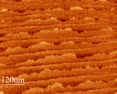
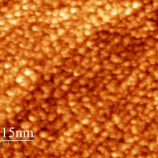
An STM image of the Si(001) surface of the buffer layer before depositing a Ge film is demonstrated in figure 1. Alternate wide terraces ending by and steps [17, 18] with smooth and jagged edges are observed on the surface as well as numerous Si adatom clusters that is characteristic to the Si(001) surfaces cooled at the quenching mode [10, 11, 19].
(a)
 (b)
(b)
 (c)
(c)
 (d)
(d)
 (e)
(e)
(a)
 (b)
(b)
(c)
 (d)
(d)
3.2 Ge film deposited at room temperature
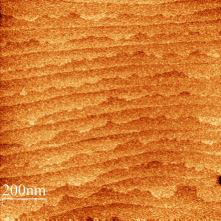
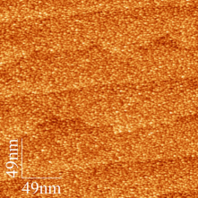
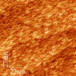
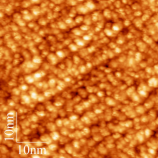
Films of Ge deposited at room temperature on the buffer layers of Si are composed of densely packed grains (figure 2). The sizes of the grains vary from less than nanometer to a few nanometers. The films are similar in their structure to the films which are formed at room temperature directly on the clean (001) surface of a silicon substrate [20]. The film is seen to be partially ordered; it is composed by relatively long nearly parallel chains consisting of tens grains. Terraces and steps of the underlaying Si buffer (both and ) are clearly seen in the STM images presented in figure 2: the granular film strictly follows the relief of the underlying surface and being smooth enough does not conceal the details of this minor roughness. This observation allows us to conclude that the obtained granular film does not reconstruct the Si buffer at least on the level of the structure of its steps.
![[Uncaptioned image]](/html/1512.01574/assets/x11.png)
(a)![[Uncaptioned image]](/html/1512.01574/assets/x12.png) (b)
Figure 4: STM images of the Ge/Si(001) wetting layer after Ge deposition at room temperature ( = 7 Å)
followed by annealing at 600 ℃ for 5 min: (a) a general view and (b) a mixed reconstruction of patches.
(b)
Figure 4: STM images of the Ge/Si(001) wetting layer after Ge deposition at room temperature ( = 7 Å)
followed by annealing at 600 ℃ for 5 min: (a) a general view and (b) a mixed reconstruction of patches.
![[Uncaptioned image]](/html/1512.01574/assets/x14.png)
(a)![[Uncaptioned image]](/html/1512.01574/assets/x15.png) (b)
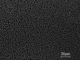
Figure 6: Microphotographs of the sample surface after Ge deposition at room temperature ( = 7 Å)
followed by annealing at 600 ℃ for 125 min; the scale marks are (a) 20 and (b) 100 µm.
(b)
Figure 6: Microphotographs of the sample surface after Ge deposition at room temperature ( = 7 Å)
followed by annealing at 600 ℃ for 125 min; the scale marks are (a) 20 and (b) 100 µm.
3.3 Ge layer annealed for 5 minutes at 600 ℃
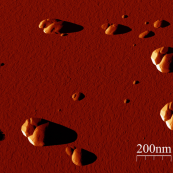
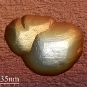
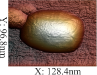
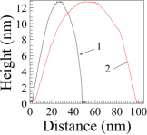
After rapid heating and isothermal annealing of the samples at 600 ℃ for 5 minutes, i.e. as a result of thermal treatment in the conditions of a closed system and in the conditions of an isolated system for the last 5 minutes, the deposited at room temperature Ge granular film reconstructs into the usual wetting layer with oval (partially faceted) Ge mounds (figures 3 and 4). The final structure coincides with that observed in the reference [20] after the same thermal processing of similar films deposited directly on the clean (001) surfaces of silicon wafers. The number density of the Ge droplets estimated from the STM images makes (1.5 to cm-2 that slightly exceeds the estimates obtained in the reference [20] (figure 3). The drops sizes usually exceed 100 nm in lateral dimensions and reach 15 nm in height. Note that there are many coalescent clusters observed on the surface; in addition, small and relatively large drops are observed simultaneously.
The wetting layer structure resembles one typical for the wetting layers formed at low temperatures (around 350℃) during MBE [6, 21, 22, 23]. Tops of the patches are composed by and reconstructed layers in close proportions (figure 4) [6, 13]. This mixed type of the wetting layer reconstruction is likely a result of a kinetically controlled transformation.
In addition to the oval drops large clusters of Ge were also detected on the surface using a light microscope (figure 5). Since their number density estimated from the microphotographs was about cm-2 a probability of their detection with STM was very low. Unfortunately, now we cannot judge about their shapes; their sizes can be estimated as at least several hundreds of nanometers. Their size distribution is at least bimodal; they often form chains.
3.4 Ge layer annealed for 125 minutes at 600 ℃
After rapid heating and isothermal annealing of the samples at 600 ℃ for 125 minutes, the large clusters of Ge increase their sizes but their distribution remains multimodal (figure 6); the number density of these clusters reduces by two orders of magnitude to cm-2 (figure 6a) however they retain some tendency to form chains (figure 6b). The largest clusters are seen to consume the substance from the surrounding smaller ones and form an empty space around themselves (figure 6a).
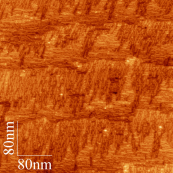
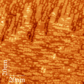
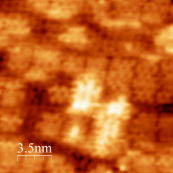
STM images do not show any presence of the oval drops on the wetting layer (figure 7). At the same time, no pyramids or domes are also observed on the surface. And evidently, wedges are not observed, either [8]. Patches of the Ge wetting layer are mainly -reconstructed. This type of the wetting layer reconstruction is characteristic to the high-temperature mode of the MBE growth of Ge on Si(001) (℃) [8]. We conclude that the reconstruction forms under the thermodynamic control and is thermodynamically favoured.
(a)
 (b)
(b)
 (c)
(c)
We believe that the observed disappearance of the Ge drops from the wetting layer after sample annealing at 600 ℃ for 125 minutes is explained by Ge redistribution in favour of the growing large clusters. Ge and Si intermixing may also affect the drop disappearance.
4 Conclusion
In summary, as a result of the short-term annealing at 600 ℃ at the described above conditions of an isolated system the Ge/Si(001) granular film deposited at room temperature transforms to the usual wetting layer and Ge clusters with multimodal size distribution with the Ge oval drops having the highest number density. After the long-term thermal treatment of the described initial samples at the same temperature, Ge drops disappear; the large clusters increase their sizes at the expense of the smaller ones. The total density of Ge clusters on the surface decreases by about four orders of magnitude. The wetting layer mixed reconstruction forming after the sort-term annealing transforms to the single one, which is likely thermodynamically favoured, as a result of the long-term annealing. Pyramids or domes are not observed on the surface after any annealing.
We cordially thank Ms N V Kiryanova for her invaluable contribution to arrangement of this research. We express our appreciation to Mr O V Uvarov for obtaining microphotographs. We also thank Ms L M Krylova for chemical treatments of the samples. The Center of Collective Use of Scientific Equipment of GPI RAS supported this research by presenting admittance to its instrumentation. We acknowledge the support of this research.
References
References
- [1] Medeiros-Ribeiro G, Kamins T I, Ohlberg D A A and Williams R S 1998 Phys. Rev. B 58 3533
- [2] Brehm M, Montalenti F, Grydlik M, Vastola G, Lichtenberger H, Hrauda N, Beck M J, Fromherz T, Schäffler F, Miglio L and Bauer G 2009 Phys. Rev. B 80 205321
- [3] Montalenti F, Raiteri P, Migas D B, von Känel H, Rastelli A, Manzano C, Costantini G, Denker U, Schmidt O G, Kern K and Miglio L 2004 Phys. Rev. Lett. 93 216102
- [4] Ross F M, Tromp R M and Reuter M C 1999 Science 286 1931
- [5] Medeiros-Ribeiro G, Bratkovski A M, Kamins T I, Ohlberg D A A and Williams R S 1998 Science 275 353
- [6] Arapkina L V and Yuryev V A 2011 J. Appl. Phys. 109 104319
- [7] Arapkina L V and Yuryev V A 2011 Nanoscale Res. Lett. 6 345
- [8] Yuryev V A and Arapkina L V 2012 J. Appl. Phys. 111 094307
- [9] Arapkina L V, Shevlyuga V M and Yuryev V A 2008 JETP Lett. 87 215–219
- [10] Arapkina L V, Yuryev V A, Chizh K V, Shevlyuga V M, Storojevyh M S and Krylova L A 2011 Nanoscale Res. Lett. 6 218
- [11] Arapkina L V, Yuryev V A, Shevlyuga V M and Chizh K V 2010 JETP Lett. 92 310–314
- [12] Arapkina L V, Krylova L A, Chizh K V, Chapnin V A, Uvarov O V and Yuryev V A 2012 J. Appl. Phys. 112 014311
- [13] Yuryev V A and Arapkina L V 2011 Nanoscale Res. Lett. 6 522
- [14] Eltsov K N, Klimov A N, Kosyakov A N, Obyedkov O V, Shevlyuga V M and Yurov V Y 2003 Chemical state and atomic structure of fcc metal surfaces in chemical reaction with halogens (Proc. of General Physics Institute vol 59) ed Konov V I and Eltsov K N (Moscow, Russia: Nauka) p 45
- [15] Horcas I, Fernandez R, Gomez-Rodriguez J M, Colchero J, Gomez-Herrero J and Baro A M 2007 Rev. Sci. Instrum. 78 013705
- [16] Arapkina L V and Yuryev V A 2010 Phys. Usp. 53 279–290
- [17] Chadi D J 1979 J. Vac. Sci. Technol. 16 1290–1297
- [18] Misbah C, Pierre-Louis O and Saito Y 2010 Rev. Mod. Phys. 82 981–1040
- [19] Yuryev V A and Arapkina L V 2013 Nanotechnology VI (Proc. SPIE vol 8766) ed Adelung R (SPIE, Bellingham, WA) p 87660M
- [20] Storozhevykh M S, Arapkina L V and Yuryev V A 2015 Nanoscale Res. Lett. 10 295
- [21] Yuryev V A, Arapkina L V, Storozhevykh M S, Uvarov O V and Kalinushkin V P 2014 J. Nanoelectron. Optoelectron. 9 196–218
- [22] Yuryev V A, Arapkina L V, Storozhevykh M S, Uvarov O V and Kalinushkin V P 2013 Nanotechnology VI (Proc. SPIE vol 8766) ed Adelung R (SPIE, Bellingham, WA) p 876606
- [23] Arapkina L V and Yuryev V A 2013 J. Appl. Phys. 114 104304