Linear magnetoresistance in compensated graphene bilayer
Abstract
We report a nonsaturating linear magnetoresistance in charge-compensated bilayer graphene in a temperature range from 1.5 to 150 K. The observed linear magnetoresistance disappears away from charge neutrality ruling out the traditional explanation of the effect in terms of the classical random resistor network model. We show that experimental results qualitatively agree with a phenomenological two-fluid model taking into account electron-hole recombination and finite-size sample geometry.
Classical magnetoresistance is a perfect tool for experimental studies of multicomponent electronic systems Pippard (1989) where conventional theory of electronic transport Abrikosov (1988) predicts a quadratic dependence of the resistance on the weak applied magnetic field followed by a saturation in classically strong fields. While most materials do exhibit the quadratic behavior,footnote there is a fast growing number of experiments reporting observations of linear magnetoresistance (LMR) in a wide variety of novel materials including multilayer graphenes Kisslinger et al. (2015); Liao et al. (2012); Friedman et al. (2010), topological insulators Pavlosiuk et al. (2015); Wiedmann et al. (2015); Ockelmann et al. (2015); Wang et al. (2013); Gusev et al. (2013); Wang et al. (2012); Wang and Lei (2012); Shekhar et al. (2012), Dirac Feng et al. (2015); Novak et al. (2015); Narayanan et al. (2015); ghimire15 ; liang15 and Weyl Shekhar et al. (2015); shekhar1506 semimetals, transition-metal dichalcogenides Zhao et al. (2015) as well as in narrow-gap semiconductors Hu and Rosenbaum (2008) and three-dimensional (3D) silver chalcogenides Husmann et al. (2002); Xu et al. (1997).
Semiclassical linear magnetoresistance has been predicted for 3D metallic slabs with complex Fermi surfaces and smooth boundaries Azbel (1963); Lifshitz et al. (1973), for strongly inhomogeneous, granular materials Parish and Littlewood (2003), and for compensated two-component systems with quasiparticle recombination Alekseev et al. (2015a). Purely quantum effects (and screening of charged impurities) lead to LMR in zero-gap band systems with linear dispersion in the case where all carriers belong to the first Landau level Abrikosov (1969, 1998); Klier et al. (2015). In weak fields, quantum interference in two-dimensional electron systems yields an interaction correction Zala et al. (2001) to resistivity that is linear in the Zeeman magnetic field.
The extreme quantum limit of Refs. Abrikosov, 1969, 1998 has been realized in graphene Friedman et al. (2010) and in Bi2Se3 nanosheets Wang et al. (2012). The quantum theory was also reported Pavlosiuk et al. (2015) to be applicable to the novel topological material LuPdBi. The classical theory of Ref. Parish and Littlewood, 2003 was recently used to interpret the behavior of hydrogen-intercalated epitaxial bilayer graphene Kisslinger et al. (2015). It was argued that large samples of epitaxial bilayer graphene contain a “built-in mosaic tiling” due to the dense dislocation networks Butz et al. (2014), making it an ideal material to realize the random network model of Ref. Parish and Littlewood, 2003. At the same time, neither theory can explain LMR in homogeneous topological insulators Veldhorst et al. (2013) and neutral two-component systems Wiedmann et al. (2015); Gusev et al. (2013); Hu and Rosenbaum (2008).
In this paper we report results of a systematic experimental analysis of magnetotransport in exfoliated bilayer graphene. Precisely at charge neutrality, we have observed nonsaturating LMR in a wide range of magnetic fields in Hall bars of widths , , and in a temperature range from to . Deviations from charge neutrality lead to eventual saturation of the magnetoresistance. Our key experimental findings are not accounted for within the random resistor network model Parish and Littlewood (2003). Indeed, this model is insensitive to the relative concentration of different types of charge carriers and thus cannot explain the observed saturation of the magnetoresistance away from charge neutrality. This model also does not explain the transition between the quadratic dependence at very weak magnetic fields and LMR observed at higher fields Wiedmann et al. (2015). The extreme quantum limit is unlikely to be reached in our system at for both electrons and holes Wiedmann et al. (2015); Veldhorst et al. (2013). Moreover, the excitation spectrum in bilayer graphene is quadratic, which rules out the quantum theory of Refs. Abrikosov, 1969, 1998.
We are able to explain our results in terms of a semiclassical description of finite-size, charge-compensated two-component systems in moderately strong, classical magnetic fields Alekseev et al. (2015a); Wiedmann et al. (2015). The key element of the physical picture of Ref. Alekseev et al., 2015a is the electron-hole recombination Abakumov et al. (1991). When external magnetic field is applied, recombination processes allow for a neutral quasiparticle flow in the lateral direction relative to the electric current Titov et al. (2013). Although such neutral current cannot be directly detected in our measurements, its presence leads to redistribution of charge carriers over the sample area influencing the nonuniform profile of the electric current in the sample. As a result, the sample is essentially split into the bulk and edge regions, which contribute to the total sheet resistance of the sample as parallel resistors. The bulk and edge resistances exhibit qualitatively different dependence on the magnetic field yielding LMR. Away from charge neutrality a nonzero Hall voltage is formed leading to the observed saturation of the magnetoresistance.
I Experimental details and sample characterization
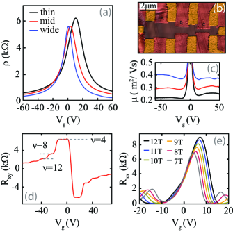
We have prepared the sample by placing the exfoliated bilayer graphene sheet on the substrate consisting of a highly doped Si wafer covered by a nm-thick SiO2 film. Subsequently, the sample was patterned into a triple Hall bar device, see Fig. 1(b) for an atomic force microscope (AFM) image. The sample consists of three sections , , and wide. The length of each Hall bar is . The sample was purified using an AFM tip (instead of annealing) which allowed us to decrease the concentration of the charged impurities on top of graphene considerably. The carrier concentration in the sample can be varied up to cm-2 by applying a gate voltage to the conducting substrate, which acts as a back gate.
Magnetotransport was studied by four-probe method with simultaneous measurements of longitudinal and transverse resistances in perpendicular magnetic fields from to and in a temperature range from to passing an ac current with an amplitude of through the sample.
To characterize the sample and to define the charge neutrality point (CNP), the field effect (FE) was measured for each section of the device. Figure 1(a) shows the FE dependences measured at and for the three sections of the device. All three sections exhibit a graphene typical FE with a sharp maximum corresponding to the CNP. The precise value of corresponding to CNP depends on the Hall bar width and is shifted from in the widest section of the sample toward in the medium and in the narrowest Hall bar. The maximum resistivity in the widest and middle sections is while exceeding for the narrowest section.
The electron and hole mobilities were estimated from the conductivity at using the one-band model (see Fig. 1(c)). The electron and hole densities necessary for this estimate were obtained from the measured Shubnikov-de Haas oscillations at low temperatures. The resulting mobilities increase with the width of the sample; we have obtained the following values for the mobilities of the narrowest, medium, and widest sections of the sample far away from charge neutrality: , , and for holes and , , and for electrons.
The dependence of the mobility on the width of the sample is attributed to scattering of carriers on the sample edges and is described in Ref.Smirnov et al., 2015. Although the above mobilities are not very high, the samples are of a good quality having a clear manifestation of CNP and exhibiting the quantum Hall effect (see Fig. 1(d)). Measurements of the Hall resistance in the wide section of the sample at in relatively high magnetic field (Fig. 1(d)) demonstrate the features inherent to bilayer graphene following from filling factors in the Hall plateaus equal to . In strong magnetic field the neutrality point is shifted towards higher gate voltages, see Figs. 1(e) and 2. For the wide section of the sample at T, CNP corresponds to . This effect has also been observed in other sections of the sample.
II Linear magnetoresistance
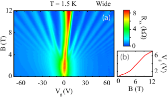
We have measured the longitudinal resistance for all three sections of the sample and the Hall resistance between widest and medium sections in the interval of gate voltages from to with the step that includes CNP for all three sections. The data for the wide section of the sample at K are shown in Fig. 2. To reduce the conductance fluctuations, further measurements were performed at higher temperatures: , , , and . At such high temperatures quantum effects, e.g. Landau quantization, are not detectable.
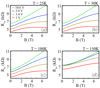
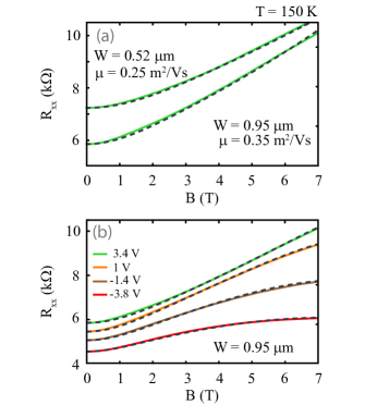
The magnetoresistance data for the thin section of the sample at the four temperatures are shown in Fig. 3. The data show linear behavior close to the neutrality point (the green curve corresponding to the gate voltage ). Away from neutrality, the data show linear behavior for an intermediate range of magnetic fields followed by a saturation at stronger fields. Similar results were obtained for the other two sections of the sample. At the same time, the Hall resistance grows in amplitude in strong fields, see Fig. 4.
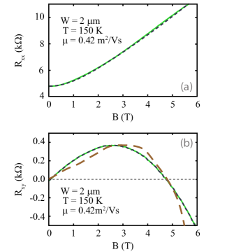
Although these observations are in good qualitative agreement with the theoretical predictions of Ref. Alekseev et al., 2015a, there are several additional factors that may (and probably do) conspire to yield the observed behavior. The charge neutrality point in our samples shifts towards higher gate voltages in high magnetic field. As a result, the same value of may correspond to different carrier densities in low and high fields. Shifting away from charge neutrality can cause both the saturation of , as exhibited by most curves in Fig. 3, and the nonzero Hall resistivity, see Fig. 4(b). The latter can also be due to electron-hole asymmetry in the sample, where the mobilities of electrons and holes are sufficiently different Poumirol et al. (2010); Zhou et al. (2014). Both effects may appear if the sample contained macroscopic inhomogeneities or resonant impurities, that strongly modify the density of states near charge neutrality. Finally, in contrast to the theory worked out in Ref. Alekseev et al., 2015a, the length of our samples is comparable to their width and the samples cannot be considered infinitely long.
| narrow | medium | wide | |
|---|---|---|---|
| W | m | m | m |
| m2/Vs | m2/Vs | m2/Vs | |
| m | m | m |
Some of the above complications present a significant challenge for an analytic theory. Nevertheless, we may attempt to analyze the measured data with the help of the existing theory of Ref. Alekseev et al., 2015a. The simplest version of this theory (applicable to a particle-hole symmetric system with parabolic dispersion and energy-independent impurity scattering rate) yields the following expressions for the longitudinal and Hall resistivities of a two-component system near charge neutrality:
| (1a) | |||
| (1b) | |||
| Here and are the charge and quasiparticle densities, is the mobility (which is assumed to be the same for both electrons and holes), is the sample width, is the zero-field resistivity, and is the field-dependent recombination length. Assuming that the dominant recombination process is the impurity-assisted electron-phonon coupling that can occur anywhere in the sample with equal probability, the recombination length found in Ref. Alekseev et al., 2015a is given by | |||
| where is the diffusion coefficient and is the recombination time in zero magnetic field. As a result, in classically strong fields () and for the magnetoresistance (1a) close to the charge neutrality point is linear, . | |||
Using the measured parameters of our sample in the above expressions, we find that the theory predicts a magnetoresistance that is stronger than what is actually observed in our experiment. However, our results can be quantitatively described by Eqs. (1a) and (1b) if we introduce an empiric expression for the recombination length
| (1c) |
with . This modification turns out Alekseev et al. (2015b) to effectively account for the following issues: (i) electron-hole asymmetry, (ii) energy dependence of the electron-hole recombination length and mobility, and (iii) spatial inhomogeneity of the sample. In Figs. 4 and 5 we used .
Electron-hole asymmetry manifests itself in the nonzero Hall resistivity at charge neutrality. Moreover, for any value of the carrier density the Hall resistivity is a nonmonotonous function of the magnetic field. As mentioned above, this effect also leads to the apparent drift of the charge neutrality point (in terms of the applied gate voltage) with the external magnetic field.
At temperatures lower than the Debye energy the dominant recombination process involves electrons and holes near the bottom of the band. Indeed, far away from the neutrality point, kinematic constraints preclude the “direct” process where an electron from the upper band is scattered into an empty state in the lower band by means of single acoustic phonon emission. Instead, such “hot” electrons require an additional scatterer (e.g. an impurity Song et al. (2012) or a second phonon) for recombination to take place. In contrast, electrons close to the neutrality point in bilayer graphene are slow enough so that the direct, single-phonon recombination is allowed. Hence, within the kinetic equation approach Alekseev et al. (2015b) the effective length scale describing the recombination processes depends on energy. Similarly, the impurity scattering time or carrier mobility is strictly speaking energy-dependent as well. Now, the macroscopic description of Ref. Alekseev et al., 2015a involves quantities that are averaged over the quasiparticle spectrum. Taking into account the existence of the several distinct recombination processes, we arrive at the conclusion that after thermal averaging, the typical recombination length may be described by slightly different effective parameters as compared to, e.g., Drude conductivity.
The width dependence of the carrier mobility indicates that the edge region of the sample is characterized by stronger scattering. As a result, all parameters describing electronic transport acquire an effective coordinate dependence across the sample. Since in strong magnetic fields the current is mostly flowing near the sample edges Alekseev et al. (2015a), we expect that the effective recombination length is determined by the lower mobility typical of the near-edge region.
Theoretical results shown in Figs. 4 and 5 were obtained by using expressions (1) with the parameters listed in Table 1. The theory (1) assumes that electrons and holes have the same mobility. While plotting Figs. 4 and 5 we have treated the mobility as a free parameter instead of using the values quoted in Sec. I (see Fig. 1(a)) since experimentally one can reliably determine mobility only far away from the neutrality point, where the classical Hall resistivity exhibits the standard behavior . Close to charge neutrality, the mobility may deviate from such experimental values due to electron-hole interaction processes similar to the drag effect. Far away from charge neutrality this interaction is ineffective since with exponential accuracy only one band is partially filled and contributes to low-energy physics. In contrast, close to the neutrality point, both electrons and holes participate in transport and hence one has to take into account their mutual scattering. The resulting change of the mobility does not exceed 50% in accordance to theoretical expectations.
The values of the recombination length shown in Table 1 show significant dependence on the sample width (roughly, ). We interpret this observation as an indication of a much larger recombination length that would characterize a very large (in theory – infinite) sample (if it were possible to fabricate without strong structural disorder Kisslinger et al. (2015); Butz et al. (2014)). Assuming that the electron-hole recombination is dominated by electron-phonon interaction (either impurity- or edge-assisted), we argue that in narrow samples the phonon spectrum is modified (compared to an idealized infinite system), leading to a much shorter recombination length of the order of the sample width.
The Hall resistance (1b) is expected to vanish at the neutrality point. However, as we have already mentioned, in our sample the neutrality point shifts toward higher gate voltages when a strong magnetic field is applied. In order to account for this effect, we have used the ratio to extract the field-dependent quantity from the experimental data. Using thus obtained dependence in Eq. (1b), we find good quantitative agreement between the calculated and measured values, see Fig. 4. At the same time, the longitudinal resistivity (1a) is much less sensitive to small deviations of density. Using the extracted values of in Eq. (1a) does not lead to visible changes in the calculated curve shown in Fig. 4.
The shift of CNP with magnetic field was observed directly, see Figs. 1 and 2. Assuming that the maximum of the longitudinal resistivity corresponds to CNP, we can extract the field dependence of the chemical potential (and hence, carrier densities) from the data. Using thus obtained dependence, we recalculated the Hall resistance, see the brown curve in Fig. 4(b). The result shows reasonable agreement with the data, with the visible deviations may stem from the mismatch of temperatures in the two data sets in Figs. 2 and 4 (K and K, respectively).
Finally, away from the neutrality point the data shows a tendency towards saturation in high magnetic fields, see Fig. 5(b). The theoretical fits where performed with a set of parameters depending on the gate voltage and taking into account the shift of CNP with magnetic field. In particular, the mobility appeared to show a slight increase from m2/Vs (close to CNP, see Table 1) to m2/Vs at V. At the same time, in that range of gate voltages the recombination length appears to be almost unchanged from the value shown in Table 1).
III Conclusions
In this paper we reported the experimental observation of linear magnetoresistance in narrow bilayer graphene samples. The observed behavior is in good qualitative agreement with the two-fluid model of Ref. Alekseev et al., 2015a. The observed effect is specific to the charge neutrality point. Away from neutrality the magnetoresistance shows an approximate linear behavior only in a limited intermediate range of magnetic fields followed by a tendency to saturation. Our observations are incompatible with the quantum theory of Refs. Abrikosov, 1969, 1998 and with the random resistor network model of Ref. Parish and Littlewood, 2003, but are accounted for in the semiclassical theory of two-component compensated systems of Ref. Alekseev et al., 2015a.
Using an empirical modification of the simplest theoretical model (1), we were able to describe our data in a quantitative fashion. A microscopic theory accounting for the physics that is beyond the simplest version of the two-fluid model of Ref. Alekseev et al., 2015a should be based on the quantum kinetic equation Alekseev et al. (2015b); Narozhny et al. (2015). Further aspects of the phenomenon of linear magnetoresistance are the subject of future experimental work, especially in numerous novel materials.
Acknowledgements.
We are grateful to U. Briskot, M. Dyakonov, A.D. Mirlin, M. Schütt, and S. Wiedmann for helpful discussions. This work was supported by the Dutch Science Foundation NWO/FOM 13PR3118, DFG SPP 1459, GIF, the EU Network Grant FP7-PEOPLE-2013-IRSES “InterNoM”, the Humboldt Foundation, the Russian Foundation of Basic Research (grant No. 15-02-04496-a, 14-02-00198 A), the Dynasty Foundation, the Grant of Russian Ministry of Education and Science (Contract No. 14.Z50.31.0021), and the President Grant for Leading Scientific Schools NSh-1085.2014.2.References
- Pippard [1989] A. B. Pippard, Magnetoresistance in metals (Cambridge, 1989).
- Abrikosov [1988] A. A. Abrikosov, Fundamentals of the theory of metals (North-Holland, Amsterdam, 1988).
- [3] In wide samples of graphene monolayers a square-root magnetoresistance has been observed in Ref. 44 near the Dirac point, resulting from the combination of linear dispersion of carriers and short-range character of scatterers [45].
- Kisslinger et al. [2015] F. Kisslinger, C. Ott, C. Heide, E. Kampert, B. Butz, E. Spiecker, S. Shallcross, and H. B. Weber, Nat. Phys. 11, 650 (2015).
- Liao et al. [2012] Z.-M. Liao, H.-C. Wu, S. Kumar, G. S. Duesberg, Y.-B. Zhou, G. L. W. Cross, I. V. Shvets, and D.-P. Yu, Advanced Materials 24, 1862 (2012).
- Friedman et al. [2010] A. L. Friedman, J. L. Tedesco, P. M. Campbell, J. C. Culbertson, E. Aifer, F. K. Perkins, R. L. Myers-Ward, J. K. Hite, J. Charles R. Eddy, G. G. Jernigan, et al., Nano Letters 10, 3962 (2010).
- Pavlosiuk et al. [2015] O. Pavlosiuk, D. Kaczorowski, and P. Wisniewski, Sci. Rep. 5, 9158 (2015).
- Wiedmann et al. [2015] S. Wiedmann, A. Jost, C. Thienel, C. Brüne, P. Leubner, H. Buhmann, L. W. Molenkamp, J. C. Maan, and U. Zeitler, Phys. Rev. B 91, 205311 (2015).
- Ockelmann et al. [2015] R. Ockelmann, A. Müller, J. H. Hwang, S. Jafarpisheh, M. Drögeler, B. Beschoten, and C. Stampfer, Phys. Rev. B 92, 085417 (2015).
- Wang et al. [2013] W. Wang, Y. Du, G. Xu, X. Zhang, E. Liu, Z. Liu, Y. Shi, J. Chen, G. Wu, and X. Zhang, Sci. Rep. 3, 2181 (2013).
- Gusev et al. [2013] G. M. Gusev, E. B. Olshanetsky, Z. D. Kvon, N. N. Mikhailov, and S. A. Dvoretsky, Phys. Rev. B 87, 081311 (2013).
- Wang et al. [2012] X. Wang, Y. Du, S. Dou, and C. Zhang, Phys. Rev. Lett. 108, 266806 (2012).
- Wang and Lei [2012] C. M. Wang and X. L. Lei, Phys. Rev. B 86, 035442 (2012).
- Shekhar et al. [2012] C. Shekhar, S. Ouardi, G. H. Fecher, A. Kumar Nayak, C. Felser, and E. Ikenaga, Applied Physics Letters 100, 252109 (2012).
- Feng et al. [2015] J. Feng, Y. Pang, D. Wu, Z. Wang, H. Weng, J. Li, X. Dai, Z. Fang, Y. Shi, and L. Lu, Phys. Rev. B 92, 081306 (2015).
- Novak et al. [2015] M. Novak, S. Sasaki, K. Segawa, and Y. Ando, Phys. Rev. B 91, 041203 (2015).
- Narayanan et al. [2015] A. Narayanan, M. D. Watson, S. F. Blake, N. Bruyant, L. Drigo, Y. L. Chen, D. Prabhakaran, B. Yan, C. Felser, T. Kong, et al., Phys. Rev. Lett. 114, 117201 (2015).
- [18] N. J. Ghimire, Y. Luo, M. Neupane, D. J. Williams, E. D. Bauer, and F. Ronning, J. Phys.: Cond. Matter 27, 152201 (2015).
- [19] T. Liang, Q. Gibson, N. Ali Mazhar, Liu Minhao, R. J. Cava , and N. P. Ong, Nature Mat. 14, 280 (2015).
- Shekhar et al. [2015] C. Shekhar, A. K. Nayak, Y. Sun, M. Schmidt, M. Nicklas, I. Leermakers, U. Zeitler, Y. Skourski, J. Wosnitza, Z. Liu, et al., Nat. Phys. 11, 645 (2015).
- [21] C. Shekhar, F. Arnold, S.-C. Wu, Y. Sun, M. Schmidt, N. Kumar, A.G. Grushin, J.H. Bardarson, R. Donizeth dos Reis, M. Naumann, M. Baenitz, H. Borrmann, M. Nicklas, E. Hassinger, C. Felser, and B. Yan, arXiv:1506.06577 (2015).
- Zhao et al. [2015] Y. Zhao, H. Liu, J. Yan, W. An, J. Liu, X. Zhang, H. Wang, Y. Liu, H. Jiang, Q. Li, et al., Phys. Rev. B 92, 041104 (2015).
- Hu and Rosenbaum [2008] J. Hu and T. F. Rosenbaum, Nat. Mater. 7, 697 (2008).
- Husmann et al. [2002] A. Husmann, J. B. Betts, G. S. Boebinger, A. Migliori, T. F. Rosenbaum, and M.-L. Saboungi, Nature 417, 421 (2002).
- Xu et al. [1997] R. Xu, A. Husmann, T. F. Rosenbaum, M. L. Saboungi, J. E. Enderby, and P. B. Littlewood, Nature 390, 57 (1997).
- Azbel [1963] M. Y. Azbel, Zh. Eksp. Teor. Fiz. 44, 983 (1963), Sov. Phys. JETP 17, 667 (1963).
- Lifshitz et al. [1973] I. M. Lifshitz, M. Y. Azbel, and M. I. Kaganov, Electron theory of metals (Consultants Bureau, New York, 1973).
- Parish and Littlewood [2003] M. M. Parish and P. B. Littlewood, Nature 426, 162 (2003).
- Alekseev et al. [2015a] P. S. Alekseev, A. P. Dmitriev, I. V. Gornyi, V. Y. Kachorovskii, B. N. Narozhny, M. Schütt, and M. Titov, Phys. Rev. Lett. 114, 156601 (2015a).
- Abrikosov [1969] A. A. Abrikosov, Zh. Eksp. Teor. Fiz. 56, 1391 (1969), Sov. Phys. JETP 29, 746 (1969).
- Abrikosov [1998] A. A. Abrikosov, Phys. Rev. B 58, 2788 (1998).
- Klier et al. [2015] J. Klier, I. V. Gornyi, and A. D. Mirlin, Phys. Rev. B 92, 205113 (2015).
- Zala et al. [2001] G. Zala, B. N. Narozhny, and I. L. Aleiner, Phys. Rev. B 65, 020201 (2001).
- Butz et al. [2014] B. Butz, C. Dolle, F. Niekiel, K. Weber, D. Waldmann, H. B. Weber, B. Meyer, and E. Spiecker, Nature 505, 533 (2014).
- Veldhorst et al. [2013] M. Veldhorst, M. Snelder, M. Hoek, C. G. Molenaar, D. P. Leusink, A. A. Golubov, H. Hilgenkamp, and A. Brinkman, Phys. Status Solidi RRL 7, 26 (2013).
- Abakumov et al. [1991] V. N. Abakumov, V. I. Perel, and I. Yassievich, in Nonradiative Recombination in Semiconductors (Elsevier, 1991), vol. 33 of Modern Problems in Condensed Matter Sciences.
- Titov et al. [2013] M. Titov, R. V. Gorbachev, B. N. Narozhny, T. Tudorovskiy, M. Schütt, P. M. Ostrovsky, I. V. Gornyi, A. D. Mirlin, M. I. Katsnelson, K. S. Novoselov, et al., Phys. Rev. Lett. 111, 166601 (2013).
- Smirnov et al. [2015] D. Smirnov, G. Y. Vasileva, J. C. Rode, Y. B. Vasilyev, Y. L.Ivanov, and R. J. Haug (2015), to be published.
- Poumirol et al. [2010] J.-M. Poumirol, W. Escoffier, A. Kumar, B. Raquet, and M. Goiran, Phys. Rev. B 82, 121401 (2010).
- Zhou et al. [2014] Y.-B. Zhou, L. Zhang, D.-P. Yu, and Z.-M. Liao, Applied Physics Letters 104, 153103 (2014).
- Alekseev et al. [2015b] P. S. Alekseev, A. P. Dmitriev, V. Y. Kachorovskii, I. V. Gornyi, M. Titov, and B. N. Narozhny (2015b), to be published.
- Song et al. [2012] J. C. W. Song, M. Y. Reizer, and L. S. Levitov, Phys. Rev. Lett. 109, 106602 (2012).
- Narozhny et al. [2015] B. N. Narozhny, I. V. Gornyi, M. Titov, M. Schütt, and A. D. Mirlin, Phys. Rev. B 91, 035414 (2015).
- [44] G. Yu. Vasileva, P. S. Alekseev, Yu. B. Vasilyev, Yu. L. Ivanov, D. Smirnov, H. Schmidt, and R.J. Haug, arXiv:1508.04009
- [45] P. S. Alekseev, A. P. Dmitriev, I. V. Gornyi, and V. Yu. Kachorovskii, Phys. Rev. B 87, 165432 (2013).