Electrical transport in nano-thick ZrTe5 sheets: from three to two dimensions
Abstract
ZrTe5 is a newly discovered topological material. Shortly after a single layer ZrTe5 had been predicted to be a two-dimensional topological insulator, a handful of experiments have been carried out on bulk ZrTe5 crystals, which however suggest that its bulk form may be a three-dimensional topological Dirac semimetal. We report the first transport study on ultra thin ZrTe5 flakes down to 10 nm. A significant modulation of the characteristic resistivity maximum in the temperature dependence by thickness has been observed. Remarkably, the metallic behavior, occurring only below about 150 K in bulk, persists to over 320 K for flakes less than 20 nm thick. Furthermore, the resistivity maximum can be greatly tuned by ionic gating. Combined with the Hall resistance, we identify contributions from a semiconducting and a semimetallic bands. The enhancement of the metallic state in thin flakes are consequence of shifting of the energy bands. Our results suggest that the band structure sensitively depends on the film thickness, which may explain the divergent experimental observations on bulk materials.
I Introduction
The topological insulator (TI) is a new quantum state of matter, which features a topologically protected metallic surface state with an insulating bulkHasan and Kane (2010); Qi and Zhang (2011). Although the first experimentally demonstrated topological insulator, HgTe quantum wellKönig et al. (2007), is a two-dimensional (2D) one, the later found three-dimensional (3D) TIs, e.g., Bi2Se3 and Bi2Te3 families, have been studied the most. This is largely due to the easiness in materials growth and the large bulk band gapChen et al. (2009); Xia et al. (2009), which are advantageous in both research and technological point of view. However, the unintentional doping of the bulk, generating a sizeable parallel electrical conduction, hinders the understanding and application of the non-trivial surface statesAnalytis et al. (2010); Checkelsky et al. (2011); Xiu et al. (2011). On the other hand, 2D TIs will not be affected by the problem owing to their gate tunabilityPribiag et al. (2015); Qu et al. (2015). Therefore, there have been great efforts in searching for new 2D TI materialsQian et al. (2014); Zhou et al. (2014); Si et al. (2014); Liu et al. (2015) and some success has been made in heterostructuresPribiag et al. (2015); Qu et al. (2015); Du et al. (2015). In light of the huge success of 2D crystals, it seems of great interest to find a 2D crystal TI material. Among many theoretical proposals, ZrTe5 has attracted immediate attention after its predictionWeng et al. (2014); Li et al. (2016a); Chen et al. (2015a, b); Zhou et al. (2015); Yuan et al. (2015); Li et al. (2016b); Moreschini et al. (2016), as it is believed to have a large band gap, meV, and it is a known material.
ZrTe5 is a layered material in which layers are stacked in the crystallographic b direction. Each layer can be seen as ZrTe6 prismatic chains in the a direction that are connected by zig-zag Te chains in the c direction. The material has been known for years, especially for its characteristic resistivity maximum at about 150 KOkada et al. (1980). The research has just revived since the prediction of ZrTe5 being a 2D TILi et al. (2016a); Chen et al. (2015a, b); Zhou et al. (2015); Yuan et al. (2015). However, the band structure remains unclear, as each among 3D Dirac semimetalLi et al. (2016a); Chen et al. (2015a, b); Yuan et al. (2015), weak TILi et al. (2016b); Wu et al. (2016) and strong TIManzoni et al. (2016), have been favored by some experiments. So far, all experimental studies have been focused on bulk ZrTe5 crystals, while no experiment on ultra thin ZrTe5 sheets has been reported. Considering the prediction of a 2D TI for monolayer, it is important to see how the property evolves with decreasing thickness. Herein, we present experimental investigation on ultra thin ZrTe5 sheets. A striking modulation of the resistivity maximum by thickness has been observed. In addition to the enhancement of metallicity with reducing thickness, the Hall resistance displays an evolution from nonlinear to linear, which clearly indicates shifting of energy bands. The ionic gating effect suggests presence of a semimetallic band, consistent with previous experiments on bulk. These observations coherently suggest that the band structure sensitively depends on the film thickness, consistent with theoretical calculationsWeng et al. (2014); Fan et al. (2016). The results provide an explanation for the divergent experimental observations on bulk materials.
II Experimental techniques
ZrTe5 single crystals were grown by an iodine vapour transfer methodOkada et al. (1980). The crystallographic structure was confirmed by X-ray diffraction and transmission electron microscopy (TEM). No trace of iodine impurities was observed in X-ray photoelectron spectroscopy. Raman spectra show the characteristics of ZrTe5. Ultra thin sheets were prepared by mechanical exfoliation onto silicon substrates with 285 nm SiO2. They can be readily identified by polarized light as the system is also quasi-one-dimensional due to the ZrTe6 prismatic chain. The thickness of sheets was measured by atomic force microscopy (AFM). Multi-electrode devices were prepared by e-beam lithography processes. Low temperature transport measurements were carried out using a standard lock-in method in a OXFORD variable temperature cryostat. Ionic gating experiment was performed using LiClO4 (Alfa Aesar,0.3g) and PEO (Alfa Aesar,1g) mixed with anhydrous methanol (Alfa Aesar,15 mL) as the solid electrolyteYu et al. (2015).
III Results and discussions
III.1 Exfoliation and stability of thin ZrTe5 flakes
The interlayer bonding in ZrTe5 is predicted to be as weak as graphite and much weaker than that in Bi2Se3 and Bi(111)Weng et al. (2014). Mechanic exfoliation is supposed to work well. However, due to its quasi-one dimensional nature, sheets are easily torn apart along the direction. Consequently, it is harder to obtain large size flakes with uniform thickness by exfoliation compared with other isotropic 2D crystals. In our experiments, flakes were often narrow in the direction, making Hall measurements not always available. Moreover, the surface of flakes mostly exhibit steps, indicating thickness variation.
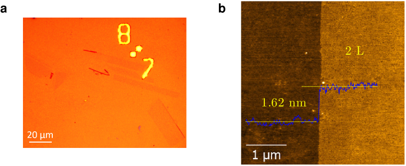
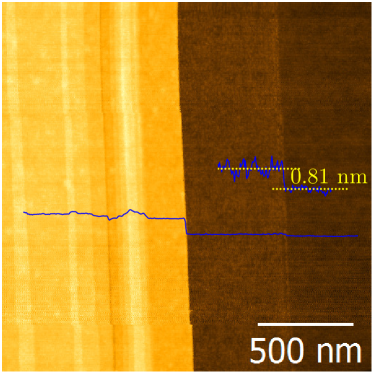
Nevertheless, in some cases, we could obtain single layer and bilayer flakes. Fig. 1a shows the optical micrograph of a few large size bilayer flakes. One of them is 60 m long. The largest one is about 20 m by 40 m, which really shows the potential to get large size few-layer flakes by exfoliation. The optical contrast for these thin flakes is extremely low so that it was hard to find them. An AFM image is shown in Fig. 1b. From the line profile, we can read the thickness, 1.62 nm, suggesting a bilayer.
Usually, using polarized light, ZrTe5 flakes can be readily identified under optical microscopy thanks to its quasi-one-dimension nature. This is done by shining a polarized light on a sample and detecting the reflected light of which the polarization is perpendicular to the incident light, i.e., crossed polarizers setup. When the axis of the sample is aligned at 45∘ with respect to the polarizers, strongest contrast can be obtained. Unfortunately, single layer and bilayer flakes didn’t exhibit any contrast. No characteristic Raman peak was found for them. They were neither conducting. These observations led us to believe that they were oxidized.
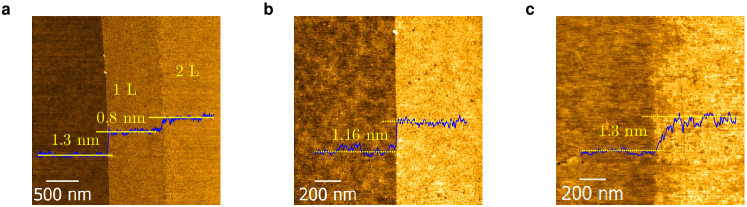
Oxidation is supported by the time evolution of the surface morphology. Fig. 2 shows the comparison of the surface morphology of flakes before and after being exposed in ambient air for 48 hours. Freshly cleaved flakes show relatively sharp edges. The rms surface roughness of the flakes is about 0.24 nm, similar to 0.2 nm for the substrate. After being exposed in air for 48 hours, the edge seemed substantially smeared and the roughness increased to 0.45 nm. Apparently, samples underwent significant changes.
III.2 Structure characterization
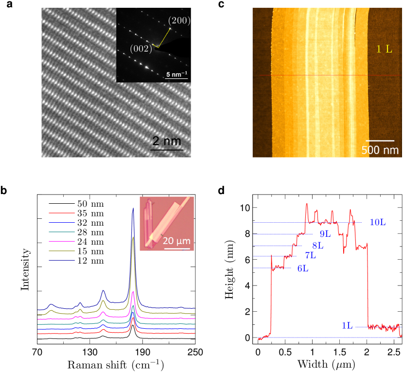
Fig. 3a shows the high resolution TEM image of a thin sheet exfoliated from a ZrTe5 crystal. The sharp diffraction spots indicate the high crystalline quality of the sample. Based on the diffraction pattern and the TEM image, we calculate the lattice constants of nm, nm. The interlayer distance is about nm estimated from the AFM results (Fig. 3d). Note that the interlayer distance determines the topological phase of ZrTe5Fan et al. (2016); Manzoni et al. (2016). Unfortunately, this cannot be done due to limited resolution of the AFM data. Raman spectra reproduce characteristic peaks reported for the materialTaguchi et al. (1983). With decreasing thickness, the frequencies of the peaks remain unchanged, whereas the intensity is markedly enhanced. Such enhancement can be explained by an interference effect due to multi-reflectionWang et al. (2008). However, the enhancement of the peak at 86 cm-1 seems much stronger than others. This mode is connected with the vibrational mode of the Te zig-zag chain and it becomes stronger at low temperatures when the material displays a metallic behaviorLanda et al. (1984). This is very similar to our experiments, where enhancement was observed for thin flakes, which are more metallic. This will be shown later. We also want to point out that the peak at 115 cm-1 is almost constant. The implications of these features are not clear and require further study. Instead, we concentrate on electrical transport. Since very thin flakes are not conducting due to oxidation, we limit our scope to sheets thicker than 10 nm.
III.3 Transport
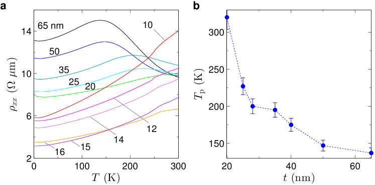
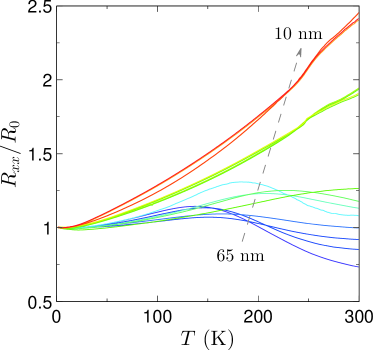
The resistivity of the thick ZrTe5 flakes as a function of temperature displays a maximum at about K, consistent with the well-known resistivity anomaly in bulk crystalsOkada et al. (1980). However, as the thickness reduces, we observe a pronounced change of . It substantially shifts to a higher temperature, shown in Fig. 4a and b. The increase of is remarkable, as it reaches 320 K at 20 nm. Below 20 nm, samples turn into metallic in the whole temperature range. The enhancement of metallicity is consonant with the change of the Raman mode at 86 cm-1.
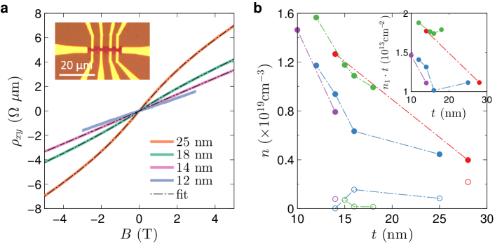
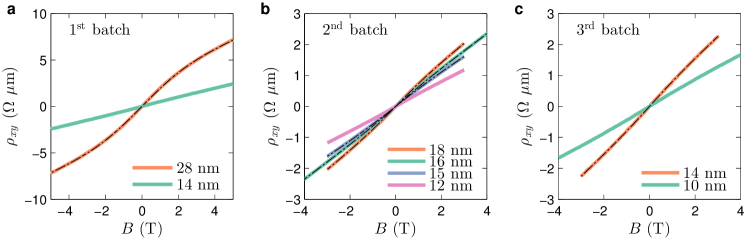
For some samples with larger size, we were able to fabricate Hall bars and measure the Hall resistance. A typical Hall bar structure is shown in the inset of Fig. 5a. For thicker samples, the Hall is nonlinear, seen in Fig. 5a, which strongly indicates carriers from more than one bands. This is not surprising as early studies on bulk have already found multiple bandsWhangbo et al. (1982); Kamm et al. (1985). Intriguingly, the nonlinearity gradually diminishes with reducing thickness. When the thickness is below 14 nm or so, it becomes linear. We have measured several batches of samples and the trend are well reproduced (see the supplementary information). Note that a linear Hall suggests dominance of a single band. Therefore, the evolution of the Hall implies a transition from multiple bands of carriers to single-band dominated carriers. Based on this observation, we have further carried out two-band fitting for the Hall. In a two-band model, the Hall resistivity
where , are the hall coefficients and , the resistivities for different bands, respectively. The total resistivity satisfies , posing an additional constraint on the fitting parameters. From this fitting, the carrier density for each band, and , are obtained by , where is the elementary charge. The fitting results are shown in Fig. 5 and Fig. S3 in the supplementary material. In Fig. 5b, the carrier density is plotted as a function of . To exclude the influence of the carrier density fluctuation among different bulk samples, we group the samples that were peeled off and patterned in the same batch. It is found that consistently increases with decreasing , while remains small and becomes relatively negligible in thin samples.
One of the unique properties of topological materials is their non-trivial surface states. Some recent spectroscopy studies have shown indications of 2D Dirac surface statesLi et al. (2016b); Wu et al. (2016); Manzoni et al. (2016). So, it is tempting to relate to the surface. In that case, the 2D carrier concentration should be more or less a constant. In the inset of Fig. 5b, is plotted against . A significant thickness dependence disfavors a surface origin. As we will explain later, is semimetallic and contributes to the metallic temperature dependence of resistivity below . If it is from the surface, its contribution in bulk materials would be too small to give rise to a substantial metallic behavior. Thus, we believe that is from the bulk. If we assume that the composition is independent of , the change of can only result from a change in the band structure, i.e., shift of the band in energy. Shifting between two semiconducting bands is ruled out, because it leads to redistribution of carriers in two bands, which is inconsistent with no significant change in . It is postulated that carriers reside in a semimetallic band resulting from band crossing and the crossing point shifts. The picture is consistent with a Dirac band observed in bulk materialsLi et al. (2016a); Chen et al. (2015a, b); Yuan et al. (2015).
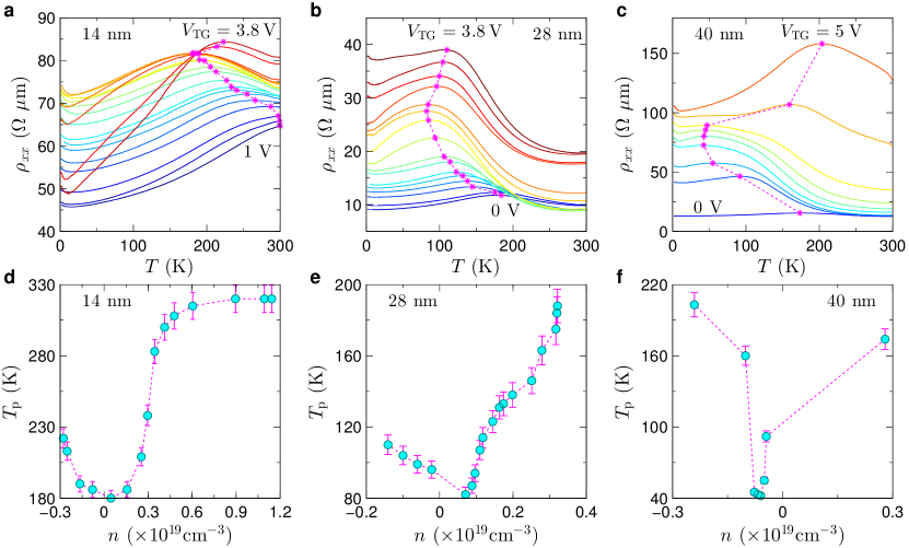
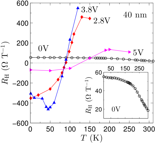
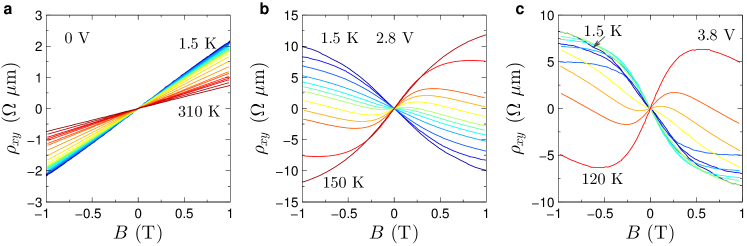
Further evidence comes from gating experiments. The advantage of having ultra-thin samples is to be able to tune the carrier density by gating. We have performed back-gating and ionic liquid top-gating. Similar results were obtained by both methods, except ionic gating offered a much larger carrier density range. Here, we mainly present the data obtained by ionic gating. The temperature dependent resistivity at different gate voltages for three samples with thickness of 14, 28 and 40 nm are plotted in Fig. 6a, b and c. With increasing gate voltage, first decreases and then increases. The non-monotonic dependence has been observed in all samples. Hall measurements have also been carried out to obtain the carrier density. A sign reverse in Hall coefficient is observed, indicating a transition of carriers from holes to electrons. is plotted against in Fig. 6d, e and f. For all three samples, the minimum occurs close to the charge neutrality point. It is worthy to note that even at the charge neutrality point, the resistivity exhibits metallic temperature dependence at low temperatures, which strongly indicates semimetallicity.
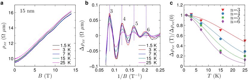
Magnetoresistance measurements reveal the nature of this semimetallic state. Fig. 7 shows the resistivity as a function of the magnetic field up to 14 T for a 15 nm thick sample. A backgate voltage of V was applied, so the carrier density is reduced. The sample shows a positivity magnetoresistance, which is often seen in Dirac materials. Similar positive magnetoresistance were observed in other samples, too. Interestingly, for this particular sample, small yet well-defined oscillations are discernible. After subtracting a smooth background, the oscillations are plotted against , which display regular periodicity, indicating Shubulikov-de Haas oscillations. The damping of the oscillation amplitude with temperature is given by the Lifshitz-Kosevich equation, , where . Here, is the Boltzmann constant, is the elementary charge and is the cyclotron mass. As depicted in Fig. 7c, we have fit the temperature dependence of the amplitude to the equation of , yielding , where is the free electron mass. Assuming a linear dispersion, we have . The Fermi velocity is estimated as m/s, in a good agreement with results reported by othersLi et al. (2016a); Chen et al. (2015a); Yuan et al. (2015). Our analysis of the quantum oscillations agrees well with experiments on bulk ZrTe5Li et al. (2016a); Chen et al. (2015a, b); Yuan et al. (2015), indicating a massless Dirac band.
III.4 Two-band model
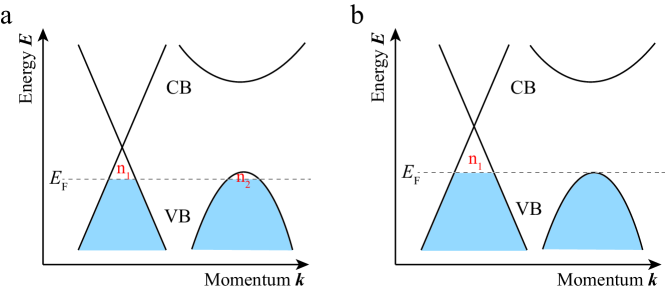
Combining all the experimental observations, a consistent picture can now be formed, shown in Fig. 8. From the thickness dependence of the Hall effect, it can be inferred that for thicker flakes, there are more than one bands at the Fermi level, which is in agreement with early studies on bulk crystalsWhangbo et al. (1982); Kamm et al. (1985). With decreasing thickness, the carrier concentration in one of the bands increases substantially. Consequently, the other band becomes negligible. The gate dependence of the Hall coefficient reveals a carrier type transition from hole to electron. Most importantly, there is no insulating state during the transition. Therefore, it can be concluded that one band is semimetallic. Analysis of the quantum oscillations is consistent with other groups’ results that the carriers in the semimetallic band are indeed massless Dirac fermions.
The thickness dependence of the Hall effect indicates shifting of energy bands. It is interesting how the thickness affects the band structure. First, we note that recent work on other 2D crystals has discovered that the charge density wave transition can be significantly affected by thicknessGoli et al. (2012); Yoshida et al. (2014); Xi et al. (2015). Recent study on MoS2 has shown that the interlayer distance increases with decreasing thickness, leading to reduction of interlayer couplingCheng et al. (2012). Second, the first principle calculation has found that the band structure is extremely sensitive to the lattice constantsWeng et al. (2014); Fan et al. (2016). In fact, experiments on bulk ZrTe5 have found that the band shifts with temperatureMcIlroy et al. (2004); Li et al. (2016a); Manzoni et al. (2015). It is therefore not surprising to see such shifting caused by thickness. We speculate that the interlayer coupling is reduced in thin flakes, due to expansion in the layer distance. To test it, measurement of the lattice constants with precision is required in future study.
Such thickness dependent band structure may offer a hint on understanding the diverse experimental observations. It has been predicted that the band structure of ZrTe5 sensitively depends on the interlayer spacingWeng et al. (2014); Fan et al. (2016). With increasing lattice constants, it undergoes a topological transition from strong TI to an intermediate Dirac semimetal and then to a weak TIFan et al. (2016). If the actual lattice constant slightly varies with the growth method, temperature or thickness, the system will end up in different topological phases. The 3D Dirac semimetal is only a point in the phase diagram against the lattice constant, so its observation at first seems unlikely. However, the observed properties around this point can be close to those of the Dirac semimetal due to finite experimental resolutionManzoni et al. (2016).
At last, we discuss the origin of the resistivity peak, which has been a mystery for ZrTe5. It was found that it coincided with a sign change of the Hall, which has led to proposals, such as charge density wave transition and polaronic conductionIzumi et al. (1982); Rubinstein (1999). However, in our thin sheets that show the resistivity peak, the Hall remains positive up to room temperature, seen in Fig. 9. This poses a strong constraint on possible models for the peak. We find that a two-band picture, one semimetallic band and one semiconducting band, naturally explains the peak feature. At low temperatures, the semimetallic band dominates the resistivity, giving rise to the metallic behaviour. With increasing temperature, the other semiconducting band takes over, due to either thermal activation or band shifting. The competition between two bands gives rise to a resistivity peak. Both bands can be of holes, as we observed in thin sheets. The change of the carrier density will alter the competition balance, hence the peak temperature, as demonstrated by the gating effect. Depending on the Fermi level, the system can shift from two hole bands to one hole band and one electron band, as shown in Fig. 9. Then, the sign change of the Hall observed in bulk is restored.
IV Conclusion
In summary, we have studied the thickness and gate dependence of the transport properties of thin ZrTe5 sheets. A strong modulation of the resistivity anomaly and a semimetallic behaviour have been observed. The Hall effect exhibits interesting dependence on the thickness. It is shown that these observations can be understood by a two-band model combined with band shifting upon thickness reduction. Our study offers a hint in understanding the divergent experimental observations on bulk.
Acknowledgements.
We are grateful for enlightening discussion with X. Dai and N. L. Wang. This work was supported by National Key Basic Research Program of China (No. 2016YFA0300600, No. 2013CBA01603, No. 2012CB933404, and No. 2016YFA0300802) and NSFC (Project No. 11574005, No. 11222436, and No. 11234001).References
- Hasan and Kane (2010) M. Z. Hasan and C. L. Kane, Rev. Mod. Phys. 82, 3045 (2010).
- Qi and Zhang (2011) X.-L. Qi and S.-C. Zhang, Rev. Mod. Phys. 83, 1057 (2011).
- König et al. (2007) M. König, S. Wiedmann, C. Brüne, A. Roth, H. Buhmann, L. W. Molenkamp, X.-L. Qi, and S.-C. Zhang, Science 318, 766 (2007).
- Chen et al. (2009) Y. L. Chen, J. G. Analytis, J.-H. Chu, Z. K. Liu, S.-K. Mo, X. L. Qi, H. J. Zhang, D. H. Lu, X. Dai, Z. Fang, S. C. Zhang, I. R. Fisher, Z. Hussain, and Z.-X. Shen, Science 325, 178 (2009).
- Xia et al. (2009) Y. Xia, D. Qian, D. Hsieh, L. Wray, A. Pal, H. Lin, A. Bansil, D. Grauer, Y. S. Hor, R. J. Cava, and M. Z. Hasan, Nat Phys 5, 398 (2009).
- Analytis et al. (2010) J. G. Analytis, R. D. McDonald, S. C. Riggs, J.-H. Chu, G. S. Boebinger, and I. R. Fisher, Nat Phys 6, 960 (2010).
- Checkelsky et al. (2011) J. G. Checkelsky, Y. S. Hor, R. J. Cava, and N. P. Ong, Phys. Rev. Lett. 106, 196801 (2011).
- Xiu et al. (2011) F. Xiu, L. He, Y. Wang, L. Cheng, L.-T. Chang, M. Lang, G. Huang, X. Kou, Y. Zhou, X. Jiang, Z. Chen, J. Zou, A. Shailos, and K. L. Wang, Nat Nano 6, 216 (2011).
- Pribiag et al. (2015) V. S. Pribiag, B. J. A., F. Qu, M. C. Cassidy, C. Charpentier, W. Wegscheider, and L. P. Kouwenhoven, Nat Nano 10, 593 (2015).
- Qu et al. (2015) F. Qu, A. J. A. Beukman, S. Nadj-Perge, M. Wimmer, B.-M. Nguyen, W. Yi, J. Thorp, M. Sokolich, A. A. Kiselev, M. J. Manfra, C. M. Marcus, and L. P. Kouwenhoven, Phys. Rev. Lett. 115, 036803 (2015).
- Qian et al. (2014) X. Qian, J. Liu, L. Fu, and J. Li, Science 346, 1344 (2014).
- Zhou et al. (2014) J.-J. Zhou, W. Feng, C.-C. Liu, S. Guan, and Y. Yao, Nano Lett. 14, 4767 (2014).
- Si et al. (2014) C. Si, J. Liu, Y. Xu, J. Wu, B.-L. Gu, and W. Duan, Phys. Rev. B 89, 115429 (2014).
- Liu et al. (2015) Q. Liu, X. Zhang, L. B. Abdalla, A. Fazzio, and A. Zunger, Nano Lett. 15, 1222 (2015).
- Du et al. (2015) L. Du, I. Knez, G. Sullivan, and R.-R. Du, Phys. Rev. Lett. 114, 096802 (2015).
- Weng et al. (2014) H. Weng, X. Dai, and Z. Fang, Phys. Rev. X 4, 011002 (2014).
- Li et al. (2016a) Q. Li, D. E. Kharzeev, C. Zhang, Y. Huang, I. Pletikosic, A. V. Fedorov, R. D. Zhong, J. A. Schneeloch, G. D. Gu, and T. Valla, Nat Phys 12, 550 (2016a).
- Chen et al. (2015a) R. Y. Chen, S. J. Zhang, J. A. Schneeloch, C. Zhang, Q. Li, G. D. Gu, and N. L. Wang, Phys. Rev. B 92, 075107 (2015a).
- Chen et al. (2015b) R. Y. Chen, Z. G. Chen, X.-Y. Song, J. A. Schneeloch, G. D. Gu, F. Wang, and N. L. Wang, Phys. Rev. Lett. 115, 176404 (2015b).
- Zhou et al. (2015) Y. Zhou, J. Wu, W. Ning, N. Li, Y. Du, X. Chen, R. Zhang, Z. Chi, X. Wang, X. Zhu, P. Lu, C. Ji, X. Wan, Z. Yang, J. Sun, W. Yang, M. Tian, and Y. Zhang, ArXiv e-prints , 1505.02658 (2015), arXiv:1505.02658 .
- Yuan et al. (2015) X. Yuan, C. Zhang, Y. Liu, C. Song, S. Shen, X. Sui, J. Xu, H. Yu, Z. An, J. Zhao, H. Yan, and F. Xiu, ArXiv e-prints , 1510.00907 (2015), arXiv:1510.00907 .
- Li et al. (2016b) X.-B. Li, W.-K. Huang, Y.-Y. Lv, K.-W. Zhang, C.-L. Yang, B.-B. Zhang, Y. B. Chen, S.-H. Yao, J. Zhou, M.-H. Lu, L. Sheng, S.-C. Li, J.-F. Jia, Q.-K. Xue, Y.-F. Chen, and D.-Y. Xing, Phys. Rev. Lett. 116, 176803 (2016b).
- Moreschini et al. (2016) L. Moreschini, J. C. Johannsen, H. Berger, J. Denlinger, C. Jozwiak, E. Rotenberg, K. S. Kim, A. Bostwick, and M. Grioni, Phys. Rev. B 94, 081101 (2016).
- Okada et al. (1980) S. Okada, T. Sambongi, and M. Ido, J. Phys. Soc. Jpn. 49, 839 (1980).
- Wu et al. (2016) R. Wu, J.-Z. Ma, S.-M. Nie, L.-X. Zhao, X. Huang, J.-X. Yin, B.-B. Fu, P. Richard, G.-F. Chen, Z. Fang, X. Dai, H.-M. Weng, T. Qian, H. Ding, and S. H. Pan, Phys. Rev. X 6, 021017 (2016).
- Manzoni et al. (2016) G. Manzoni, L. Gragnaniello, G. Autès, T. Kuhn, A. Sterzi, F. Cilento, M. Zacchigna, V. Enenkel, I. Vobornik, L. Barba, F. Bisti, P. Bugnon, A. Magrez, V. N. Strocov, H. Berger, O. V. Yazyev, M. Fonin, F. Parmigiani, and A. Crepaldi, Phys. Rev. Lett. 117, 237601 (2016).
- Fan et al. (2016) Z. Fan, Q.-F. Liang, Y. B. Chen, S.-H. Yao, and J. Zhou, ArXiv e-prints (2016), 1611.04263 .
- Yu et al. (2015) Y. Yu, F. Yang, X. F. Lu, Y. J. Yan, ChoYong-Heum, L. Ma, X. Niu, S. Kim, Y.-W. Son, D. Feng, S. Li, S.-W. Cheong, X. H. Chen, and Y. Zhang, Nat Nano 10, 270 (2015).
- Taguchi et al. (1983) I. Taguchi, A. Grisel, and F. Levy, Solid State Commun. 46, 299 (1983).
- Wang et al. (2008) Y. Y. Wang, Z. H. Ni, Z. X. Shen, H. M. Wang, and Y. H. Wu, Appl. Phys. Lett. 92, 043121 (2008).
- Landa et al. (1984) G. Landa, A. Zwick, R. Carles, M. Renucci, and A. Kjekshus, Solid State Commun. 49, 1095 (1984).
- Whangbo et al. (1982) M. H. Whangbo, F. J. DiSalvo, and R. M. Fleming, Phys. Rev. B 26, 687 (1982).
- Kamm et al. (1985) G. N. Kamm, D. J. Gillespie, A. C. Ehrlich, T. J. Wieting, and F. Levy, Phys. Rev. B 31, 7617 (1985).
- Goli et al. (2012) P. Goli, J. Khan, D. Wickramaratne, R. K. Lake, and A. A. Balandin, Nano Lett. 12, 5941 (2012).
- Yoshida et al. (2014) M. Yoshida, Y. Zhang, J. Ye, R. Suzuki, Y. Imai, S. Kimura, A. Fujiwara, and Y. Iwasa, Sci. Rep. 4, 7302 (2014).
- Xi et al. (2015) X. Xi, L. Zhao, Z. Wang, H. Berger, L. Forró, J. Shan, and K. F. Mak, Nat. Nanotechnol. 10, 765 (2015).
- Cheng et al. (2012) Y. Cheng, Z. Zhu, and U. Schwingenschlögl, RSC Adv. 2, 7798 (2012).
- McIlroy et al. (2004) D. N. McIlroy, S. Moore, D. Zhang, J. Wharton, B. Kempton, R. Littleton, M. Wilson, T. M. Tritt, and C. G. Olson, J Phys : Condens Matter 16, L359 (2004).
- Manzoni et al. (2015) G. Manzoni, A. Sterzi, A. Crepaldi, M. Diego, F. Cilento, M. Zacchigna, P. Bugnon, H. Berger, A. Magrez, M. Grioni, and F. Parmigiani, Phys. Rev. Lett. 115, 207402 (2015).
- Izumi et al. (1982) M. Izumi, K. Uchinokura, E. Matsuura, and S. Harada, Solid State Commun. 42, 773 (1982).
- Rubinstein (1999) M. Rubinstein, Phys. Rev. B 60, 1627 (1999).
Supplemental Materials: Electrical transport in nano-thick ZrTe5 sheets: from three to two dimensions
The temperature dependence of resistivity for thicker samples ( nm) shows clearly a hump at a certain temperature range from 145 K to 295 K, while for thin flakes (less than 15 nm) it exhibits a metallic behavior in the whole range of temperature below about 320 K. With decreasing thickness, a prominent shift of from low to high temperature can be observed.
The thickness dependence of the carrier density implies at least two bands involved for thick flakes. This is also supported by deviation of the Hall resistivity from linearity in higher magnetic fields. Fig. S3 shows the Hall resistivity as a function of the magnetic field, they were well fitted with the two-band model. As explained in the text, we have grouped samples according to their batch numbers. When flakes are thick, displays a nonlinear behavior. In contrast, when the thickness is less than about 15 nm, they are rather linear, indication of contribution from a single band. This trend appears in all batches, suggesting a transition from a two-band structure to a single band. This is consistent with the proposed band picture, i.e., shifting one band away and leaving only one band at the Fermi level.
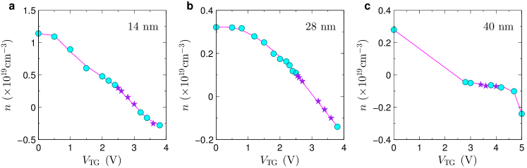
The carrier density can be calculated from the Hall resistivity . The ionic gating experiments demonstrate a transition of carriers from holes to electrons, similar to graphene. Ideally, at the transition point, one should observe a divergent and a sudden jump from positive to negative, as is inversely proportional to the carrier density . In reality, increases to a finite value and then gradually reverses to negative due to density fluctuations. So, in the transition region, it is not appropriate to estimate from any more. Therefore, we have obtained in this region by interpolation, as indicated in Fig. S4.
Early studies have found that the resistivity anomaly concurs with a sign change of the Hall resistivity and thermopower, indication of a change of the carrier type from electrons to holes. The observation led to speculations that the anomaly could result from the change of the band structure which also leads to the change of the carrier type[34,40]. However, our results show presence of the resistivity anomaly without change of the carrier type, see Fig. 9. We show that the competition between a Dirac semimetallic band and a semiconducting hole band can explain the resistance and Hall very well. Fig. S5 plots the Hall resistivity at 0, 2.8 and 3.8 V, from which the carrier density in Fig. 9 were obtained. When 2.8 and 3.8 V, it can be seen that is negative at low temperature and become positive at high temperatures, similar to that of bulk material. Furthermore, is strongly nonlinear, suggesting two bands.