Simultaneous observation of small- and large-energy-transfer electron-electron scattering in three dimensional indium oxide thick films
Abstract
In three dimensional (3D) disordered metals, the electron-phonon (e-ph) scattering is the sole significant inelastic process. Thus the theoretical predication concerning the electron-electron (e-e) scattering rate as a function of temperature in 3D disordered metal has not been fully tested thus far, though it was proposed 40 years ago [A. Schmid, Z. Phys. 271, 251 (1974)]. We report here the simultaneous observation of small- and large-energy-transfer e-e scattering in 3D indium oxide thick films. In temperature region of K, the temperature dependence of resistivities curves of the films obey Bloch-Grüneisen law, indicating the films possess degenerate semiconductor characteristics in electrical transport property. In the low temperature regime, as a function of for each film can not be ascribed to e-ph scattering. To quantitatively describe the temperature behavior of , both the 3D small- and large-energy-transfer e-e scattering processes should be considered (The small- and large-energy-transfer e-e scattering rates are proportional to and , respectively). In addition, the experimental prefactors of and are proportional to and ( is the Fermi wave number, is the electron elastic mean free path, and is the Fermi energy), respectively, which are completely consistent with the theoretical predications. Our experimental results fully demonstrate the validity of theoretical predications concerning both small- and large-energy-transfer e-e scattering rates.
pacs:
73.23.-b, 73.20.Fz, 72.15.QmI Introduction
Four decades ago, the inelastic scattering of the electrons of an impure metal by a screened Coulomb interaction had been investigated.ref1 It had been found that the electron-electron (e-e) scattering rate in three dimensional (3D) disordered metal can be expressed as,ref1 ; ref2 ; ref3
| (1) |
where is Fermi energy, is the Fermi wave number, is the mean free path of electrons, is the temperature, is the Boltzmann constant and is the Planck constant divided by 2. The first and second terms on the right hand side of Eq. (1) represent the large- and small-energy-transfer e-e scattering processes and dominate at energy scale and , respectively, where is the electron elastic mean free time.ref2 ; ref3 However, the validity of Eq. (1) has not been completely testedref4 ; ref5 ; ref6 ; ref7 ; ref8 due to the e-e scattering is negligible compared with electron-phonon (e-ph) scattering in general 3D disordered metals.ref9 ; ref10 ; ref11 Taking advantage of the low concentration and free-electron-like electrical transport properties of charge carrier in Sn doped In2O3 (ITO),ref12 ; ref13 Zhang et al recently tested the correctness of the small-energy-transfer term in Eq. (1) in ITO thick films.ref14 In the present paper, we fully demonstrate the validity of Eq. (1) (including both large- and small-energy-transfer terms) in In2O3 thick films. Our results concerning the electrical transport properties and dephasing mechanism of this low carrier concentration and large material are presented and discussed below.
II Experimental methods
In2O3 films were deposited on the (100) yttrium stabilized ZrO2 (YSZ) single crystal substrates by standard rf-sputtering method. An In2O3 target with purity of 99.99% and diameter of 60 mm was used as the sputtering source. The base pressure of chamber was less than Pa, and the sputtering was carried out in argon atmosphere with pressure of 0.55 Pa. In the depositing process, the substrate temperature was kept at 703, 723, 743, 763, 803, 823, 843, and 923 K, respectively, to tune the charge concentration and the disorder degree of the film. Hall-bar-shaped samples (1-mm wide and 3.6-mm long), deposited by using metal masks,ref14 ; ref15 were used to measure the electrical transport properties. The thicknesses of the films ranging from 950 nm to 1100 nm were measured using a surface profiler (Dektak, 6M). The structures of the films were determined by x-ray diffraction (XRD) with Cu radiation. The measurements include normal -, , and scans. The XRD results indicate that the films are epitaxially grown on (100) YSZ substrates along [100] direction. The Hall coefficient, longitudinal resistivity and low-field magnetoconductivity were measured on a physical property measurement system (PPMS-6000, Quantum Design) by four-probe method. In the magnetoconductivity measurements, the magnetic field was applied perpendicular to the film plane.
| Film | (300 K) | (10 K) | ||||||||||
|---|---|---|---|---|---|---|---|---|---|---|---|---|
| (K) | (nm) | (m cm) | (K) | ( cm-3) | ( s-1) | (K-3/2 s-1) | (K-2 s-1) | (K-3/2 s-1) | (K-2 s-1) | |||
| 1 | 703 | 1093.60 | 1.52 | 1456 | 8.9 | 3.83 | 0.88 | 1.28 | 3.02 | 1.23 | 4.27 | |
| 2 | 723 | 1068.36 | 2.50 | 1399 | 5.3 | 4.06 | 14.2 | 1.69 | 2.81 | 2.64 | 4.11 | |
| 3 | 743 | 1050.98 | 2.55 | 1399 | 5.1 | 3.91 | 1.74 | 1.61 | 2.67 | 2.79 | 4.21 | |
| 4 | 763 | 1067.45 | 2.37 | 1373 | 5.6 | 4.26 | 23.9 | 1.52 | 2.54 | 2.38 | 3.97 | |
| 5 | 803 | 1033.56 | 1.89 | 1365 | 6.7 | 4.92 | 16.6 | 1.37 | 2.43 | 1.72 | 3.61 | |
| 6 | 823 | 1002.18 | 1.67 | 1313 | 7.9 | 4.71 | 20.9 | 1.20 | 2.32 | 1.37 | 3.72 | |
| 7 | 843 | 1016.62 | 1.50 | 1335 | 8.5 | 5.22 | 1.84 | 1.20 | 2.24 | 1.20 | 3.47 | |
| 8 | 923 | 952.93 | 1.31 | 1236 | 9.1 | 6.31 | 2.43 | 1.15 | 1.87 | 1.01 | 3.06 |
III Results and Discussion
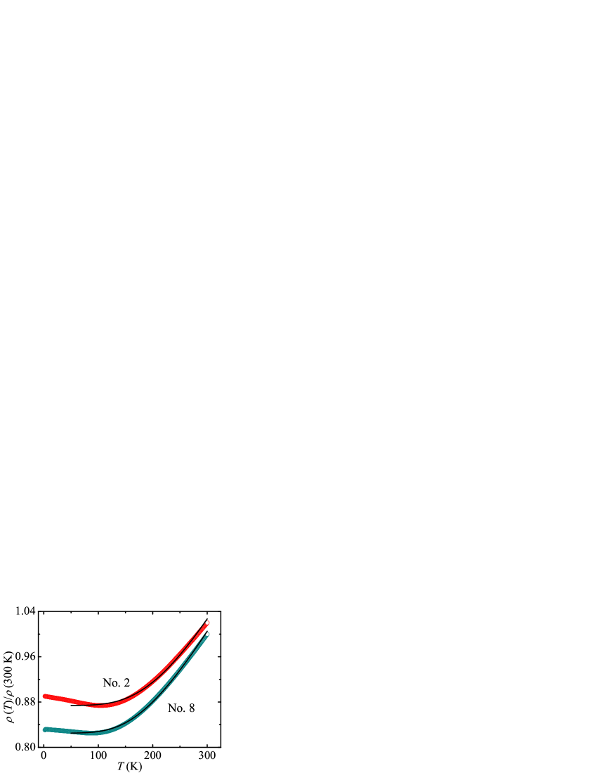
Figure 1 shows the resistivity as a function of temperature for two representative In2O3 films, as indicated. The resistivities decrease with decreasing temperatures from 300 to 100 K, reach their minimum and then increase with further decreasing temperature down to our minimum measuring temperature, 2 K. We compare the data at higher temperature region with Bloch-Grüneisen lawref16
| (2) |
where is the residual resistivity, is a constant, is the Debye temperature. The solid curves in Fig. 1 are least-squares fits to Eq. (2). The resistivity data can be well described by Eq. (2), indicating In2O3 films possess highly degenerate semiconductor characteristic in electrical transport properties. The fitted values of are listed in Table 1. Similar to Sn doped In2O3ref12 and F doped SnO2,ref17 our In2O3 films also possess higher Debye temperature. The enhancement in resistivity with decreasing temperature below 100 K can be attributed to the weak-localization (WL) and electron-electron interaction effects,ref18 ; ref19 ; ref20 ; ref21 ; ref22 which is similar to that in ITOref8 ; ref12 and FTO.ref17 The temperature behavior of resistivity of the In2O3 films in higher temperature regime indicate In2O3 possesses degenerate semiconductor characteristic in transport properties. In fact, the origins of the high conductivity and degenerate semiconductor characteristic of In2O3 are still enigmatic. The oxygen vacancy is generally considered as the main contribution to the high conductivity of the undoped In2O3.ref23 ; ref24 ; ref25 ; ref26 ; ref27 ; ref28 ; ref29 ; ref30 However, recent theoretical results indicate that the donor level of oxygen vacancies is too deep to produce large densities of free electrons at room temperature.ref31 The reasons that In2O3 possesses relative high carrier concentration and behaves as degenerate semiconductor in electrical transport properties deserve further investigations.
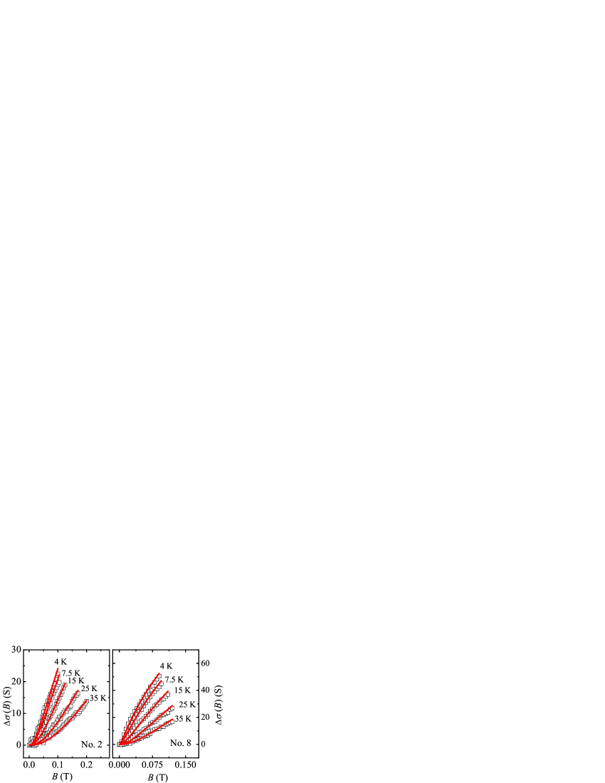
Figure 2 shows the magnetoconductivity, , as a function of magnetic field at low temperatures (4-35 K) for two representative films, as indicated. We found that the magnetoconductivity is positive and its magnitude at a certain field decrease with increasing temperature. These features indicate that the spin-orbit scattering is weak, and the WL effect governs the behaviors of at low field region.ref9 ; ref21 ; ref22 Considering the thicknesses of all samples are 1 m, we analyse the magnetoconductivity data using 3D WL theory. In 3D disordered conductors, the magnetoconductivity due to WL effect is given byref32 ; ref33 ; ref34 ; ref35 ; ref36
| (3) |
where is the elementary charge, is the diffusion constant, and . The characteristic field is defined by , where and i represent the -independent and inelastic scattering fields ( is the corresponding relaxation time), respectively. The theoretical predictions of Eq. (3) are least squares fitted to our magnetoconductivity data and are shown as solid curves in Fig. 2. Our magnetoconductivity data can be well described by Eq. (3). For the samples, the obtained electron dephasing length at 4 K varies from 90 to 380 nm, which much less than the thicknesses of the films. Hence our films are 3D with regard to WL effect.
Figure 3 shows the extracted electron dephasing rate as a function of for the two representative films, as indicated. As mentioned above, the e-ph scattering is the dominant electron dephasing mechanism in 3D general disordered metals.ref9 ; ref10 ; ref11 Assuming the e-ph scattering mechanism governs the electron dephasing processes of the films, we quantitatively analyze the data now. Theoretically, the electron scattering by transverse vibrations of defects and impurities dominates the e-ph relaxation. In the quasiballistic limit of (where is the wave number of a thermal phonon), the relaxation rate, , is given byref37 ; ref38
| (4) |
where = is the electron-transverse phonon coupling constant, is the Fermi momentum, is the transverse sound velocity, is the mass density, and is the electronic density of states at the Fermi level. For our films, the values of vary from to .note1 , which are greater than unity for K. Our data from 4 to 35 K were least-squares fitted to the following equation:
| (5) |
where stands for the saturated dephasing rate,ref39 ; ref40 ; ref41 and is an adjustable parameter and presumably represents the e-ph scattering strength given in Eq. (4). The dash curves in Fig. 3 are the fitted results. Clearly, the experimental dephasing rate can be described by the term at high temperature regime ( K), while it deviate from the predication of Eq. (5) for K. The fitted values of vary from to K-2 s-1. On the other hand, the values of and of In2O3 are 2400 m s-1 and 7100 kg m-3,ref42 respectively, the carrier concentrations vary from to cm-3, and the effective mass of electron can be taken as ,ref43 where is the free-electron mass. According to Eq. (4), one can readily obtain that the theoretical values of e-ph scattering strength [the prefactor of in Eq. (4)] vary between to K-2 s-1, which are two orders of magnitudes less than the values of . Thus the e-ph scattering rate is negligibly weak in our 3D In2O3 films.
In the framework of free-electron model, one can deduce the e-ph relaxation rate from Eq. (4), where is the carrier concentration. However, Eq. (1) predicates and , where and represent the large- and small-energy-transfer e-e relaxation time, respectively. For the In2O3 films, the carrier concentration is around cm-3, which is 3 to 4 orders of magnitudes less than that of typical metals. Hence the e-e scattering rate could be much greater than the e-ph scattering rate in this low carrier concentration compound. The data were then least-squares fitted to the following equation:
| (6) |
where the second and third terms on the right-hand side of Eq. (6) stand for the small- and large-energy-transfere-e scattering terms, respectively. The solid curves in Fig. 3 are the theoretical predication of Eq. (6). Inspection of Fig. 3 indicates that the experimental dephasing rate can be well described by Eq. (6) in the whole measuring temperature range. The obtained values of and , as well as , are listed in Table 1. Using free-electron-like model, one can easily obtain the theoretical values of and [see Eq. (1)] , denoted as and and also listed in Table 1, respectively. For most of the films, the values of are nearly equal to the theoretical ones, except for films Nos. 2, 3 and 4. Even for the three films, the values of and agree to within a factor of 2 or smaller. Also, our experimental values of are within a factor of 1.6 of . These levels of agreement are satisfactory. Thus, both the small- and large-energy-transfer e-e scattering processes govern the dephasing in these 3D In2O3 films. Inspection the experimental values of and indicates that the large-energy-transfer e-e dephasing rate is about one-half of that of the small-energy-transfer one even at 5 K for each film.
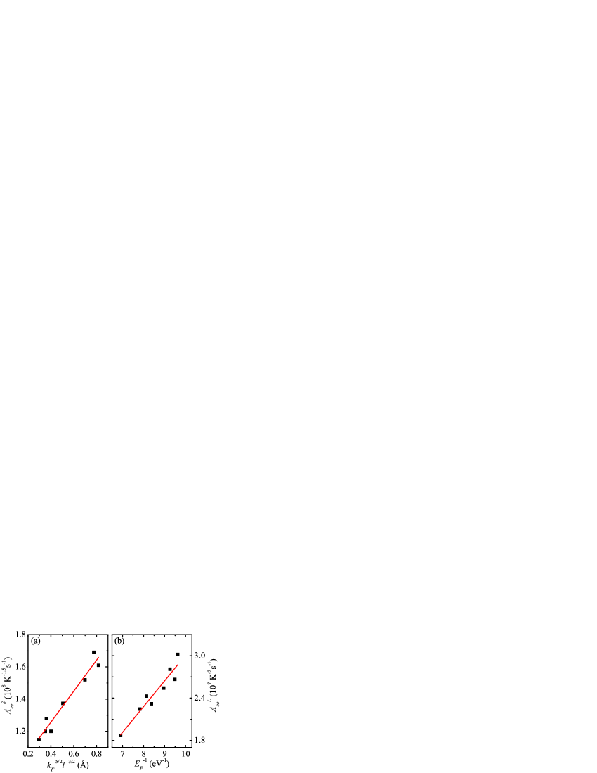
According to Eq. (1), the parameters and in Eq. (6) should obey and , respectively. (In free-electron-like approximation, should obey .) Figures 4(a) and 4(b) show variation with and as a function of , respectively. Here the values of , and are also determined from the free-electron-like model. As expected, the and rules are observed in Fig. 4. According to Eq. (1), the slopes of - and - curves should be 3.41 m-1 K-3/2 s-1 and 7.10 J K-2 s-1, respectively. The least-squares fits results indicate the slopes being m-1 K-3/2 s-1 and 5.84 J K-2s-1, respectively. The experimental value of the slope of - curve is 18% smaller than the theoretical one. The consistency between the two values is extremely good. While the experimental and theoretical values of the slope of - curve agree to within a factor of 3. This level of agreement is also satisfactory.
As mentioned above, the carrier concentrations of the In2O3 films are cm-3, which are 3-4 orders of magnitude lower than that in typical metals. Hence the e-ph relaxation rates of the In2O3 films are greatly suppressed and the e-e scattering rates are much enhanced. The value of the In2O3 film is about twice as large as that in ITO films used in Ref. ref14, , while the carrier concentration of the former is about one fourth of that of the latter. Since the Fermi energy , the small-energy-transfer e-e scattering strength of the In2O3 film would be much less than that of the ITO film used in Ref. ref14, , while the large-energy-transfer e-e scattering strength in the former would be great than that in the latter (see Eq. (1)). That is why the electron dephasing process in ITO films is only governed by the small-energy-transfer e-e scattering and both the large- and small-energy-transfer e-e scattering process have to be considered in In2O3 films. In a word, theses characteristics of relative large and low carrier concentrations of In2O3 thick films give us opportunity to simultaneously observe small- and large-energy-transfer electron-electron scattering in 3D disordered conductors, and for the first time fully demonstrate the 3D - scattering rate deduced 40 years ago.
IV Conclusion
We have studied the temperature behavior of resistivity and the electron dephasing rate in low temperature regime in In2O3 thick films. The data obey Bloch-Grüneisen law from 300 down to 100 K, indicating the films possess degenerate semiconductor characteristic in electrical transport properties. The e-ph scattering rate is negligibly week though the In2O3 films are 3D with regard to WL effect. On the contrary, the e-e inelastic scattering govern the low temperature dephasing processes. In addition, besides the small-energy-transfer e-e scattering, the large-energy-transfer e-e scattering also has significant contribution to the total electron relaxation rate. Our results also quantitatively demonstrate the validity of the theoretical predications of both small- and large-energy-transfer e-e scattering rates in experiment.
Acknowledgements.
This work was supported by the National Natural Science Foundation of China (NSFC) through Grant No. 11174216, Research Fund for the Doctoral Program of Higher Education through Grant No. 20120032110065.References
- (1) A. Schmid, Z. Phys. 271, 251 (1974).
- (2) B. L. Altshuler and A. G. Aronov, JETP Lett. 30, 482 (1979).
- (3) B. L. Altshuler and A. G. Aronov, in - , edited by A. L. Efros and M. Pollak (Elsevier, Amsterdam, 1985).
- (4) Z. Ovadyahu, Phys. Rev. Lett. 52, 569 (1984).
- (5) A. Stolovits, A. Sherman, K. Ahn and R. K. Kremer, Phys. Rev. B 62, 10565 (2000).
- (6) T. Andrearczyk, J. Jaroszyski, G. Grabecki, T. Dietl, T. Fukumura and M. Kawasaki, Phys. Rev. B 72, 121309R (2007).
- (7) T. Dietl, T. Andrearczyk, A. Lipiska, M. Kiecana, M. Tay and Y. Wu, Phys. Rev. B 76, 155312 (2000).
- (8) X. D. Liu, E. Y. Jiang, and D. X. Zhang, J. Appl. Phys. 104, 073711 (2008).
- (9) J. J. Lin and J. P. Bird, J. Phys.: Condens. Matter 14, R501 (2002).
- (10) J. Rammer and A. Schmid, Phys. Rev. B 34, 1352 (1986).
- (11) Y. L. Zhong and J. J. Lin, Phys. Rev. Lett. 80, 588 (1998).
- (12) Z. Q. Li and J. J. Lin, J. Appl. Phys. 96, 5918 (2004).
- (13) J. J. Lin and Z. Q. Li, J. Phy.: Condens. Matter 26, 343201 (2014).
- (14) Y. J. Zhang, Z. Q. Li, and J. J. Lin, Europhys. Lett. 103, 47002 (2013).
- (15) Y. J. Zhang, Z. Q. Li and J. J. Lin, Phys. Rev. B 84, 052202 (2011).
- (16) J. M. Ziman, (Clarendon Press, Oxford, 1960), p. 364.
- (17) W. J. Lang and Z. Q. Li, Appl. Phys. Lett. 105, 042110 (2014).
- (18) S. P. Chiu, J. G. Lu, and J. J. Lin, Nanotechnology 24, 245203 (2013).
- (19) B. L. Altshuler, D. Khmelnitzkii, A. I. Larkin, and P. A. Lee, Phys. Rev. B 22, 5142 (1980).
- (20) P. A. Lee and T. V. Ramakrishnan, Rev. Mod. Phys. 57, 287 (1985).
- (21) G. Bergmann, Phys. Rep. 107, 1 (1984).
- (22) Int. J. Mod. Phys. B 24, 2015 (2010).
- (23) S. Lany and A. Zunger, Phys. Rev. Lett. 98, 045501 (2007).
- (24) F. A. Kröger, The Chemistry of Imperfect Crystals (North-Holland, Amsterdam, 1974), 2nd ed.
- (25) J. H. W. de Wit, J. Solid State Chem. 13, 192 (1975).
- (26) J. H. W. de Wit, G. van Unen, and M. Lahey, J. Phys. Chem. Solids 38, 819 (1977).
- (27) A. Ambrosini, G. B. Palmer, A. Maignan, K. R. Poeppelmeier, M. A. Lane, P. Brazis, C. R. Kannewurf,T. Hogan, and T. O. Mason, Chem. Mater. 14, 52 (2002).
- (28) P. Agoston, K. Albe, R. M. Nieminen, and M. J. Puska, Phys. Rev. Lett. 103, 245503 (2009).
- (29) S. Lany and A. Zunger, Phys. Rev. Lett. 106, 069601 (2011).
- (30) P. Agoston, K. Albe, R. M. Nieminen, and M. J. Puska, Phys. Rev. Lett. 106, 069602 (2011).
- (31) S. Lany, A. Zakutayev, T. O. Mason, J. F. Wager, K. R. Poeppelmeier, J. D. Perkins, J. J. Berry, D. S. Ginley, and A. Zunger, Phys. Rev. Lett. 108, 016802 (2012).
- (32) A. Kawabata, Solid State Commun. 34, 431 (1980).
- (33) A. Kawabata, J. Phys. Soc. Jpn. 49, 628 (1980).
- (34) H. Fukuyama and K. Hoshino, J. Phys. Soc. Jpn. 50, 2131 (1981).
- (35) C. Y. Wu and J. J. Lin, Phys. Rev. B 50, 385 (1994).
- (36) D. V. Baxter, R. Richter, M. L. Trudeau, R. W. Cochrane, and J. O. Strom-Olsen, J. Phys. Paris 50, 1673 (1989).
- (37) A. Sergeev and V. Mitin, Phys. Rev. B 61, 6041 (2000).
- (38) Y. L. Zhong, A. Sergeev, C. D. Chen, and J. J. Lin, Phys. Rev. Lett. 104, 206803 (2010).
- (39) The value of is evaluated through , where is the transverse sound velocity.
- (40) J. J. Lin and N. Giordano, Phys. Rev. B 35, 1071 (1987).
- (41) P. Mohanty, E. M. Q. Jariwala, and R. A. Webb, Phys. Rev. Lett. 78, 3366 (1997).
- (42) S. M. Huang, T. C. Lee, H. Akimoto, K. Kono, and J. J. Lin, Phys. Rev. Lett. 99, 046601 (2007).
- (43) T. Wittkowski, J. Jorzick, H. Seitz, B. Schroder, K. Jung, and B. Hillebrands, Thin Solid Films 465, 398 (2001).
- (44) I. Hamberg, C. G. Granqvist, K. F. Berggren, B. E. Sernelius, and L. Engström, Phys. Rev. B 30, 3240 (1984).