Probe-based data storage
Abstract
Probe-based data storage attracted many researchers from academia and industry, resulting in unprecedented high data-density demonstrations. This topical review gives a comprehensive overview of the main contributions that led to the major accomplishments in probe-based data storage. The most investigated technologies are reviewed: topographic, phase-change, magnetic, ferroelectric and atomic and molecular storage. Also, the positioning of probes and recording media, the cantilever arrays and parallel readout of the arrays of cantilevers are discussed. This overview serves two purposes. First, it provides an overview for new researchers entering the field of probe storage, as probe storage seems to be the only way to achieve data storage at atomic densities. Secondly, there is an enormous wealth of invaluable findings that can also be applied to many other fields of nanoscale research such as probe-based nanolithography, 3D nanopatterning, solid-state memory technologies and ultrafast probe microscopy.
I Introduction
For more than 50 years, the search for technologies that offer ever increasing densities of digital data storage has been successful. Of all solutions, probe-based data storage has attracted a lot of attention over the past decades. In this overview, a wide variety of probe storage implementations is discussed and many initial experiments are shown. A few implementations have been matured further, and, in the case of thermomechanical storage, this led to a first prototype in 2005***http://www.physorg.com/news3361.html, last accessed at 21 March, 2015. with, for that time, revolutionary areal densities of . Since then, demonstrations of much higher densities have been published, showing that probe storage can outperform any other storage technology.
Probe storage is attractive because the bit size is not determined by the maximum resolution of lithographical processes, which become increasingly costly: Probes can be chemically etched and have the potential to be atomically sharp without expensive manufacturing steps.
The main challenge of probe storage is to scale up a single probe operated under laboratory conditions to large probe arrays working at high speeds in consumer products. When increasing the number of probes, the positioning accuracy has to be maintained, also under externally applied shocks and ambient-temperature variations. Fabrication-induced deviations between the probes in the array have to be minimized to ensure that all probes function correctly and remain working throughout the device life-time. The medium and the tips have to endure many read-write cycles, and the tips must be able to travel for kilometers over the storage medium.
I.1 Schematic of probe-storage system
A schematic of an architecture for a storage device based on probe technology is shown in Figure 1. This kind of architecture was first proposed by IBM Lutwyche1999 . The core of the storage device is an array of probes with a moving medium on the opposite side. Each probe can locally alter a property of the medium to write a bit. Reading is accomplished by the same probe that wrote the bit.
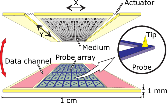
A variation on the architecture shown in Figure 1 uses a spinning disk, as in hard-disk drives, to position the medium. Such a design offers constant high positioning speeds. Spinning disks are mainly researched in combination with ferroelectric probe storage Zhao2008 ; Hiranaga2009 .
I.2 Current status of probe storage
The maturity of the various types of probe storage differs significantly. Four popular types, namely phase change, magnetic, thermomechanical and ferroelectric storage are listed in table 1.
| Phase-change | Magnetic | Thermomech. | Ferroelectric | |
|---|---|---|---|---|
| Density | Hamann2006 | Kappenberger2009 | Wiesmann2009 | Tanaka2010 |
| Est. Max. density | Wright2006 | Kryder2008 | Wiesmann2009 | Cho2005 |
| Read speed per probe | Hamann2006 | Onoue2008 | Sebastian2009 | Hiranaga2009 |
| Write speed per probe | Hamann2006 | Onoue2008 | Cannara2008 | Cho2006 |
| Travel per probe | Bhaskaran2009 | Onoue2008 | Lantz2009 | Tayebi2010 |
Probe-based data storage has attracted much scientific and commercial interest Yang2007b ; Wright2011 ; ProbeStorageChap2011 . After more than two decades of research on probe storage, an overview of what has been accomplished so far, together with an outlook of the potential of probe storage, is presented in this overview. The time seems right to assess the results because most large industrial efforts devoted to probe storage have been discontinued in the past years. The focus has shifted towards new applications that exploit the technology developed for probe storage. Examples of such applications are probe lithography Garcia2014 , nanofabrication and 3D nanopatterning Pires2010 .
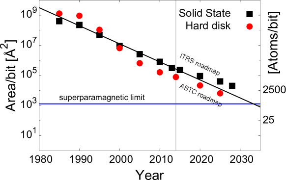
Is it time to write off probe storage completely and learn from what has been accomplished? Recently, progress in the increase in areal densities has slowed down, both in electronically addressed (solid-state) memories and in mechanically addressed storage (Figure 2). Inevitably, however, the issue of thermal stability in hard-disk storage will force a transition to other storage principles. This transition will have to occur in the next one or two decades. Currently, probe storage remains the only potentially viable route to achieving densities beyond those of the hard-disk.
I.3 Paper outline
This review is an updated and expanded version of parts of the book chapter ‘Probe Storage’ ProbeStorageChap2011 and is targeting the nanoscale aspects of a probe-storage system. It is divided into three sections: probe and medium technologies (section II), positioning systems (section III), and probe arrays and parallel readout (section IV). The probe and medium technologies section is split into subsections according to the different physical methods of storing data. In each such subsection, first the type of storage is introduced, then the write and read processes and the storage media are described. Finally, endurance is discussed, as it remains a key issue in further maturing probe technologies.
The positioning systems section is devoted to the positioning of the storage medium relative to the probe array. Different types of actuators are compared in terms of their suitability for a probe-storage system. The probe arrays and parallel readout section discusses the challenges in scaling up from a single probe as used in scanning probe microscopy to 2D probe arrays as required for probe storage.
II Probe and medium technologies
In this section, we discuss the various principles of storing and reading data. We can distinguish a number of categories, each with its own physical parameter that is locally modified to store data: (1) topographic storage uses a topographical change, (2) phase-change storage in chalcogenide materials (e.g., Ge2Sb2Te5) uses a change in the phase of the material from amorphous to crystalline and vice versa, (3) phase-change storage on non-chalcogenide materials uses two distinct material phases, (4) magnetic storage uses magnetization, (5) ferroelectric storage uses electrical polarization, (6) atomic and molecular storage uses the relative orientation of atoms. Especially this last technology has a strong potential for future work on probe storage.
II.1 Topographic storage
The most mature probe storage technology is topographic storage, mainly developed by IBM in a project termed ‘millipede’ Vettiger2000 ; Knoll2006 . A thermomechanical process creates a topographical change in a polymer medium. The change is, in the most straightforward implementation, an indentation that represents a 1. The absence of the indentation is used both as a spacer between neighboring 1s and for denoting a 0.
II.1.1 Data writing
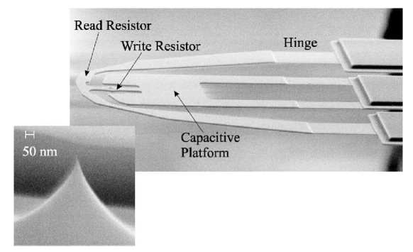
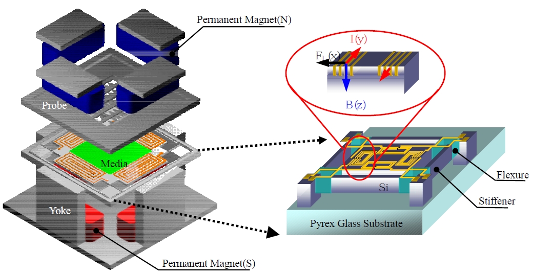
Writing is accomplished by heating the tip of the probe and applying an electrostatic force to the body of the cantilever, thereby pulling the tip into the medium. The tip is heated by means of a localized heater at its base, see Figure 3. The heater consists of a low-doped resistive region of silicon that acts as heating element. This writing process has been demonstrated to be capable of megahertz writing speeds at densities above Cannara2008 .
The development of this thermomechanical write process in polymers started with the early work of Mamin et al. Mamin1992 . They used an external laser to supply the heat to the cantilever stylus and achieved heating times of and data rates of . The integration of the heater in the cantilever initially led to an increase of the heating time to . A later design by King et al. resulted in a decrease in the heating time down to King2001 . This design was realized using a combination of conventional and e-beam lithography Drechsler2003 . The cantilevers in this design were long and only thick, yielding extremely low spring constants of . The size of the heater platform was reduced down to , resulting in time constants on the order of . The writing energy was less than per bit, mainly because of parasitic effects and an inappropriate measurement setup, so there is potential for improvement. The storage density is defined by the medium properties, and, more importantly, also by the probe tip dimensions. Lantz et al. tried to achieve higher densities by applying multiwalled carbon nanotube tips with a tip radius down to . The advantage of the carbon nanotube tips is that the tip radius does not increase by wear, instead the tip just shortens. Densities of up to were reached Lantz2003 , which was disappointing because at that time densities up to could already be attained with ultrasharp silicon tips. However, the power efficiency was improved because of better heat transfer through the nanotube. Data could be written at heater temperatures of lower than with comparable silicon tips.
II.1.2 Data reading
To read back the data, a second resistor is present in one of the side-arms of the three-legged cantilever design, see Figure 3. This resistor acts as temperature-dependent resistor, whereby an increasing temperature causes a higher resistance. The read resistor is heated, and the amount of cooling is accelerated by proximity to the medium. When the tip reaches an indentation, the medium is closer to the read resistor and thus the current that flows through the resistor will increase. The data is read back by monitoring this current. The platform is heated to about , well below the temperature needed for writing, and a sensitivity of is obtained Durig2000 .
Thermal readout was investigated in more detail by King et al., who showed that the fraction of heat transferred through the tip/medium interface is very small and most of the heat flow passes across the cantilever-sample air gap King2002 . This observation presented the possibility of heating a section of the cantilever to avoid reading with heated tips, which can cause unwanted erasures and increased medium wear. Simulations were performed to optimize the probe design. A shorter tip increased the sensitivity to King2001 .
To guide and speed up the design of more sensitive probes and assist in the readout data analysis, Dürig developed a closed-form analytical calculation for the response of the height sensor Durig2005 . An optimized design by Rothuizen et al. led to a bandwidth of several tens of kHz at powers on the order of Rothuizen2009 . Later, by using feedback, the read speed of the optimized design could be increased from to Sebastian2009 .
II.1.3 Recording medium
The first polymer media used for thermomechanical storage were simply -mm-thick PMMA (perspex) disks Mamin1992 . Using a single cantilever heated by a laser through the PMMA disk, Mamin et al. were able to write bits having a radius below and a depth of , enabling data densities of up to . In subsequent work, the bulk PMMA or polycarbonate (compact disk material) disks were replaced by silicon wafers on top of which a -nm PMMA recording layer on top of a -nm cross-linked hard-baked photoresist were deposited. This allowed small bit dimensions down to , and data densities of up to were shown Binnig1999 . In addition to PMMA, also other polymers were studied, such as polystyrene and polysulfone Vettiger2002 . A write model was developed by Dürig (Figure 18 in Vettiger2002 ). From the model, it became clear that a balance needs to be found between stability and wear resistance of the medium on the one hand, requiring highly cross-linked polymers Gotsmann2006b , and wear of the tip on the other hand, for which a soft medium is necessary.
Based on this knowledge, a so-called Diels-Adler (DA) polymer was introduced Gotsmann2006 . These DA polymers are in a highly cross-linked, high- molecular-weight state at low temperature, but dissociate at high temperature into short strains of low molecular weight. This reaction is thermally reversible: rather than a glass-transition temperature, these polymers have a dissociation temperature. Below the transition temperature, the polymer is thermally stable and has a high wear resistance; above the transition temperature the polymer becomes easily deformable and is gentle on the tip. Using the new DA polymer, densities of up to were demonstrated Gotsmann2006 .
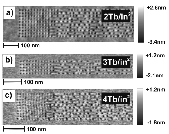
The work was continued with a polyaryletherketone (PAEK) polymer, which incorporates diresorcinol units in the backbone for control of the glass-transition temperature and phenyl-ethynyl groups in the backbone and as endgroups for cross-linking functionality Wiesmann2009 . As with the DA polymer, this polymer is highly crosslinked to suppress media wear during reading and to enable repeated erasing. In contrast to the DA polymer, however, it has a conventional, but very low, glass-transition temperature of less than in the cross-linked state, enabling indentation on a microsecond time scale using heater temperatures of less than . It exhibits exceptional thermal stability up to , which is crucial for minimizing thermal degradation during indentation with a hot tip. Using this polymer, densities of up to have been achieved on ultra-flat polymers made by templating the polymer on a cleaved mica surface Pires2009 ; Knoll2010b , see Figure 4. Modeling shows that in this type of polymer media the density is limited to Wiesmann2009 . The polymer crosslink density and topology have been optimized, leading to experimental demonstrations of density and write cylces using the same tip Gotsmann2010 . The optimized polymer was shown to endure erase cycles and read cycles and featured an extrapolated 10 year retention at . Another approach is to introduce an ultrathin elastic coating to optimize the mechanical stability of the underlying polymer film Kaule2013 . A plasma-polymerized norbornene layer physically separates the plastically yielding material from the material in contact with the tip. Both tip and medium wear are reduced, while retaining retention of the indentations written.
Apart from IBM, also others have been investigating polymer media. Kim et al. from LG demonstrated bit diameters of in PMMA films Kim2005 . Bao et al. of the Chinese Academy of Sciences investigated friction of tips with varying diameters on PMMA, and concluded that blunt tips can be used to determine the glass-transition temperature, whereas -nm-diameter tips can be used to detect local () transitions Bao2008 .
II.1.4 Endurance
Endurance poses one of the largest problems for a probe storage system. Much work has been done to mitigate tip wear, which is the main issue that needs to be overcome to obtain a reasonable device life-time. To get a feel for the extent of the problem of tip wear, a description of the wear issue in thermomechanical storage is taken from Lantz2009 . Consider a system operating at and a data-rate of per probe. With the data storage industry life-time standard of 10 years and continuous operation of the device, each probe slides a distance of 10 to . This translates into a maximum tolerable wear rate on the order of one atom per 10 m sliding distance in order to maintain the density. When operated in normal contact mode on a polymer medium, a silicon tip loaded at wears down in , sliding to a bluntness that corresponds to data densities of .
A first estimate of the tip-sample force threshold at which wear starts to become an issue was given by Mamin et al. Mamin1995 . A load force of is mentioned to maintain reliable operation for the relatively large-sized indentations () described in this early work. Such a force is detrimental for any reported probe-medium combination when densities above are targeted. In a more exhaustive study on wear by Mamin et al. Mamin1999 , a bit diameter of is shown to be maintained throughout a tip travel length of . Although the tip travel length is sufficient for a probe storage device, the bit diameter is far from competitive.
Several ways to reduce tip wear in thermomechanical recording have been proposed and demonstrated. Three important measures are discussed here.
A first measure to reduce the tip wear is softening of the medium, e.g., by the inclusion of a photo-resist layer of between the silicon substrate and the storage medium (PMMA) Binnig1999 . Various other measures to reduce tip wear from the medium side have been investigated, see Section II.1.3 for details.
Hardening of the probe is a second way of mitigating tip wear. Coating the tip with a hard material or molding a tip generally leads to larger tip radii. The wear resistance of probes was reduced using diamond-like carbon tips to bring down wear to only one atom per every micrometer of tip sliding Bhaskaran2010 . A further improvement was achieved by Lantz et al. using SiC tips Lantz2012 . For thermomechanical storage, silicon is therefore preferred Lantz2009 .
A third way to reduce the tip wear is by actuation of the tip with a periodic force at frequencies at or above the natural resonant frequency of the cantilever. It is known from AFM that the intermittent-contact mode of operation reduces tip wear, and this is one of the foremost reasons that intermittent contact is preferred over contact mode in many microscopy environments. Application of the intermittent-contact mode for probe storage is not very straightforward. There are many requirements on the probes, and some of them conflict with the requirements for intermittent contact, e.g., the high cantilever stiffness required for intermittent-contact AFM conflicts with the feeble cantilever used in thermomechanical storage to allow easy electrostatic actuation. The speed of intermittent-contact modes is also reported to be insufficient for probe storage Lantz2009 . In Ref. Sahoo2008 , a solution is presented that uses amplitude modulation of the cantilever through electrostatic actuation despite a high nonlinearity in the cantilever response. The authors show successful read and write operation at densities after having scanned . A second solution is to slightly modulate the force on the tip-sample contact. Lantz et al. Lantz2009 showed that by application of a sinusoidal voltage between the cantilever and the sample substrate, tip wear over a sliding distance of is reduced to below the detection limit of the setup used. Knoll et al. Knoll2010 use a similar actuation voltage between sample and tip to achieve a so-called dithering mode that is shown to effectively prevent ripples on a soft polymer medium. The authors attribute the absence of the otherwise present ripples to the elimination of shear-type forces by dithering at high frequencies.
II.2 Phase-change storage on chalcogenide media
Phase-change storage is well-known from optical disks, for which laser light is used to modify phase-change materials, such as GeSbTe, to store information. Data storage is performed by locally changing an amorphous region to a crystalline region and vice versa. This transition is accompanied not only by a significant change in reflectivity, which is exploited for optical disks, but there is also a change in resistivity over several orders of magnitude. Major work has been done on probe recording on phase-change media at Matsushita Tohda1995 ; Kado1997 , Hokkaido University Gotoh2004 , CEA Grenoble Bichet2004 ; Gidon2004 , the University of Exeter Wright2006 ; Wright2003 ; Aziz2005 ; Wright2008 ; Wright2010 ; Wang2011 ; Wang2014 ; Wang2014a , and Hewlett-Packard Naberhuis2002 .
II.2.1 Data writing
Phase-change recording in probe storage uses an electrical current to induce the heat required. A conductive probe passes a current through the storage medium. The current locally heats the medium and, at sufficiently high temperatures, a transition from the amorphous to the crystalline phase is induced. This write process is self-focusing, resulting in bit densities greater than Gidon2004 . The power consumption for the writing process is low with respect to other technologies (smaller than per bit written Satoh2006 ). This is because only the bit volume, and not the entire tip volume, is heated. There are, however, alternative strategies in which the tip itself is heated. Lee et al. used a resistive heater to increase the tip temperature and write crystalline bits Lee2002a . Hamman et al. achieved an impressive density of by heating the AFM probe with a pulsed laser diode Hamann2006 . The authors anticipate write speeds of for one probe when using a spinning disk to position the medium (as in hard-disk drives) and a nanoheater instead of the pulsed laser diode. Rewriteability is demonstrated by erasing part of the written data using a focused laser diode. The dynamics of the AFM tip is too slow to realize the fast thermodynamics needed for amorphization. In general, amorphizing phase-change materials with a probe is very challenging Bhaskaran2009c . Phase-change storage offers the possibility for more advanced write strategies, such as multi-level recording Burr2010 and mark-length encoding Wright2010 . The latter holds promise to increase user densities by at least and potentially as much as .
At the Tohoku University, Lee et al. used dedicated heater tips to write bits into AgInSbTe films Lee2002a . Readout was achieved by measuring the local conductance of the medium.
II.2.2 Data reading
The most common method of data read back is to measure the conductance of the medium by applying a low potential on the probe and monitoring the current. If the probe is in direct contact with the medium, one essentially performs conductive AFM Bichet2004 . Also non-contact modes exist that rely on changes in either the field-emitter currents Naberhuis2002 or the tip-sample capacitance by Kelvin probe force microscopy Nishimura2002 . The difference in material density between the amorphous and the crystalline phase can also be exploited. The crystalline phase has a higher density, causing a bit written in an amorphous background to appear as a valley that is several angstroms deep Bichet2004 ; Gidon2004 . The topographic map of the surface can be obtained by standard tapping-mode AFM Hamann2006 .
II.2.3 Recording medium
Phase-change recording media have mainly been researched for storage on optical disks and currently form an active field of research for non-volatile memory applications. Thorough overviews of solid-state phase-change memory are given in Burr2010 and in Wong2010 . A map for phase-change recording materials has been developed Lencer2008 and their properties have been reviewed in detail Wuttig2007 .
II.2.4 Endurance
Tip wear is quite a severe issue because not only the tip sharpness has to be maintained, but also the tip’s ability to conduct. Tips for phase-change recording have been successfully made more wear-resistant by changing the fabrication material. The deposition of platinum on a silicon tip and subsequent annealing create a hard layer of platinum silicide Bhaskaran2009a . An ingenious way to strengthen the tip is encapsulation of the conductive platinum silicide tip with a relatively large layer of silicon oxide. The pressure on the tip apex is now decreased because of the increase of the tip area. The resolution of storage is, however, still determined by the small conductive core Bhaskaran2009 ; Bhaskaran2009b . Such a design leads to more stringent demands on the medium side, as the larger tip apex will typically generate larger forces at the tip-sample interface, thereby potentially wearing down the medium. Force-modulation schemes are shown to be beneficial for the endurance of conductive probes. Moreover, it has been demonstrated that when using force modulation lower, load forces are needed to obtain a good electrical tip-medium contact Koelmans2010a ; Koelmans2011 . Given the severe limitations in writing amorphous regions in phase-change materials, the prospects for probe-based phase-change storage are dim. The application of probes on phase-change media is, however, very useful to study material properties at the nanoscale, and much of the insight gained for probe-storage purposes can be applied in this context.
II.3 Phase-change storage on non-chalcogenide media
Although most work is done on chalcogenide materials, a number of alternatives exist and are briefly summarized here.
Instead of phase-change media based on inorganic compounds, such as GeSbTe alloys, one can use polymers that become conductive upon application of a voltage Takimoto1997 . The change in conductivity can be due to a change in the phase, caused for instance by polymerization Shi2000 , or due to electrochemical reactions esashi2005 ; yoshida2005 ; yoshida2007 . The latter method is especially interesting as it is reversible. The exact nature of the reaction is unknown; it could be either an oxidation-reduction or protonation-deprotonation reaction. Polymer media are softer than alloys, and tip wear is expected to be less of an issue Yoshida2013 . Rewritability, however, could be a problem because the polymer tends to polymerize. Rather than heating the phase-change material by passing a current from tip to sample, one can use heated tips.
Phase-change storage without the use of heat has been demonstrated at Jo2009 . The researchers from LG Electronics and Pohang University in Korea use the tip to apply pressure alone, causing microphase transitions of the polystyrene-block-poly (n-pentyl methacrylate) of a block copolymer.
II.4 Magnetic storage
Magnetic recording is one of the oldest data-storage technologies, and many researchers have attempted to write on magnetic media with probes. The reasons are simple: Magnetic recording materials are readily available, and in recording labs, the Magnetic Force Microscope (MFM) is a standard instrument.
II.4.1 Data writing
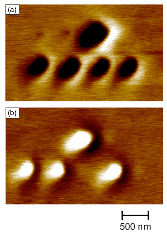
The stray field of MFM probes is relatively low, which limits the maximum achievable density to about Mironov2009 . Moreover, dots can only be magnetized in the direction of the tip magnetization. Under these constraints, however, MFM writing has been beautifully demonstrated by Mironov et al. Mironov2009a . Writing experiments have been performed in a vacuum MFM on Co/Pt multi-layered dots with perpendicular anisotropy. Two samples were investigated, one with a dot diameter of and a periodicity of , and the other with a diameter of and a spacing of . The large dots could be written by moving the MFM tip in contact over the medium. The -nm dots could be written by merely touching the dots with the MFM tip.
To write onto modern recording media at higher density, some type of assist will be necessary. There are essentially two methods: applying a uniform external background field or applying heat.
An external field can easily be applied by means of a small coil mounted below the medium. As early as 1991, Ohkubo et al. used permalloy tips on a CoCr film for perpendicular recording Ohkubo1991 ; Ohkubo1993 ; Ohkubo1993a . By applying the field in opposite directions, the magnetization of the tip can be reversed, and higher bit densities can be obtained by partially overwriting previously written bits. Bit sizes down to could be obtained Ohkubo1995 , and overwriting data was possible. Similar bit sizes were obtained by Manalis Manalis1995 using a CoCr alloy and CoCr- or NiFe-coated tips.
The bit sizes are relatively large, limiting data densities to somewhere on the order of . This is either due to the media used or the limited resolution of the MFM tip. Detailed analyses by El-Sayed showed, however, that densities up to should be possible with a rather conventional -nm tip radius El-Sayed2003 ; El-Sayed2004 .
Onoue et al. showed that care must be taken when applying high voltages to coils below the medium. If the medium is not grounded, a large capacitive charging current will flow from the tip into the sample, unintentionally heating the medium Onoue2008 and resulting in relatively large bits. Without grounding, no bits could be written because of the high switching field distribution in the Co/Pt multilayer used.
To increase the tip’s stray field, Kappenberger et al. produced Co rod-like tips of diameter by means of electrodeposition inside a porous alumina membrane Kappenberger2009 . The tip apex was tailored down to a diameter by means of focused ion-beam etching. Using this tip and a UHV MFM, they performed write experiments in 60-nm-diameter dots deposited on nano-spheres spaced by (which would be equivalent to ). Even though the tip’s stray field was expected to be large, a background field of still had to be applied to reverse the magnetization.
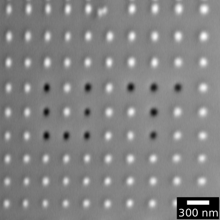
Another example of tip-field-induced writing in bit-patterned media is shown in Figure 5. The medium is based on a Co/Pt multilayered film with perpendicular anisotropy, patterned by Laser Interference Lithography DeVries2013 . Because the switching field distribution of the magnetic islands is larger than the tip’s stray field, several tricks had to be applied. A uniform external magnetic field was applied under an angle of to achieve the lowest possible switching field distribution. First, a field sweep is performed to determine the order of switching of the islands. The pattern is then written in such a way that the islands that switch at the highest field are written first. For this, the external magnetic field is increased to a value just below the switching field of the island. The combined field of the external uniform field and the tip’s stray field then reverses only this island. To maximize the effect of the tip’s stray field, the tip is lowered several times to the island in closely spaced points, while the MFM slow-scan direction is slightly modulated. This ensures that uncertainties in the tip position are compensated and that occasional domains are pushed out of the island Mironov2009 . Once the strongest island has been written, the external field is slightly reduced and the procedure repeated until the last island has been reversed.
Rather than applying background fields and incurring the risk of erasing previous information, one can locally heat the medium to reduce its switching field. This is a method also suggested for future hard-disk systems with extremely high-anisotropy media Ruigrok2000 ; Seigler2008 .
In contrast to hard-disk recording, it is surprisingly easy to deliver heat to the medium in probe storage. The most straightforward method for heating is to pass a current from the tip to the medium. Watanuki et al. Watanuki1991 used an STM tip made from an amorphous magnetic material around which a coil was wound. The tip-sample distance was controlled by the tunneling current. Bit sizes on the order of were achieved.
For testing purposes, one does not even have to use a magnetic tip or apply a background field: When starting from a perpendicularly magnetized film, the demagnetization field of the surrounding film will reverse the magnetization in the heated area. This procedure allows write-once experiments. Hosaka et al. experimented with writing bits into magnetic films by passing a current from an STM tip into a Co/Pt multilayer with perpendicular anisotropy. The minimum domain size, observed by optical microscopy, was 250 nm Hosaka1995 ; Nakamura1995 , but smaller domains might have been present. The experiment was repeated by Zhang et al. but now the bits were imaged by MFM Zhang2007 ; Zhang2006 ; Zhang2006a ; Zhang2006b ; Zhang2006c ; Zhang2006d ; Zhang2004 . Bits sizes down to were observed in Co/Pt multi-layers and weakly coupled CoNi/Pt granular media by Zhong Zhong2007 .
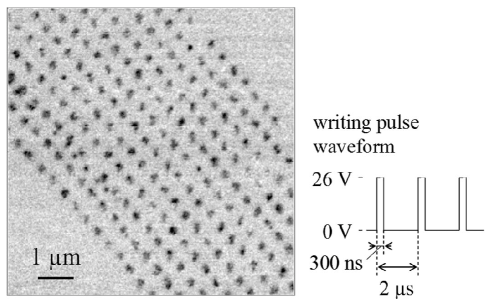
The large disadvantage of using STM tips is that direct imaging of written bits is only possible by spin-polarized tunneling, which is a difficult technique. Using MFM tips, imaging can be done immediately after writing. Hosaka et al. used an MFM tip in field-emission mode Hosaka1995 and wrote bits as small as . Onoue et al. combined this method with applying a pulsed background field Onoue2004 ; Onoue2005 , so that bits could also be erased Onoue2008 (Figure 6). The minimum bit size obtained was , which is close to the bubble collapse diameter for the Co/Pt films used in these experiments Onoue2008 .
Rather than using currents, one can also use heated tips, similar to those used on the polymer media described above. Algre et al. proposed to write by means of a heated AFM tip Algre2005a . They start from a Co/Pt multilayer patterned medium prepared by sputtering on pillars of diameter, spaced apart. The pillars were etched into nano-porous silicon to achieve good thermal insulation. The authors show that these media are suitable for heat-assisted magnetic probe recording. The readout method is, however, not clear, and the authors do not demonstrate actual recording experiments.
II.4.2 Data reading
Readback of magnetic information can be done by techniques based on MFM. MFM being a non-contact mode, however, the operation is complex. More importantly, the resolution is determined by the tip-sample distance. This distance has to be smaller than the bit period, i.e., on the order of or less. At this distance, non-magnetic tip-sample interactions become important, leading to undesired topographic cross-talk. A straightforward solution would be to use a Hall sensor integrated on a magnetic tip Sarajlic2010 ; Petit2004 ; Oral1996 ; Gregusova2009 ; Hatakeyama2014 . For better signal-to-noise ratios, integration of a magneto-resistive sensor at the end of the probe, similarly as in hard-disk recording, is preferred. An initial step in this direction was taken by Craus et al. using scanning magnetoresistance microscopy Craus2005 . The magnetic layer in the probe can be used as a flux-focusing structure, so that the same probe can be used for writing. A more advanced spin-valve sensor was integrated on a cantilever by Takezaki et al. Takezaki2006 . The resolution was limited to about , which is insufficient for probe-based data storage. Magnetic field sensors integrated in modern hard disks are, however, capable of resolutions far below , so in principle, the technique could be applied.
II.4.3 Recording medium
The data density in magnetic recording media is primarily determined by the thermal stability of the written information. The energy density in these media is relatively low compared with other media (on the order of ), so the problem was first recognized in the field of magnetic storage Charap1997 . In essence, the energy barrier between the two information states – in magnetic recording the states are two opposing magnetization directions – should be much higher than the thermal energy. At room temperature, this means that the energy barriers should be higher than , or approximately , which is a convenient value to remember. The energy barrier is determined by the energy density in the magnet and the volume of the bit. With increasing density, the bit volume decreases, so the energy density in the material should increase. The highest energy density known to us () is found in SmCo alloys Lectard1994 . At this value, the minimum magnetic volume for stable storage is approximately . Developments in hard-disk storage are targeting storing one bit of information in this tiny volume, for instance by using bit-patterned media Lodder2004 ; Terris2007 or by using aggressive coding techniques to store a bit in one or two magnetic grains Wood2009 . If successful, the maximum user storage-density (this means after coding) imaginable with magnetic recording will be on the order of a few Kryder2008 , which is indicated at the super-paramagnetic limit in Figure 2. Magnetic probe-storage demonstrations, however, have been limited to a density on the order of a few . In view of the fact that values of up to have already been demonstrated in polymer-based media Knoll2010b , the question arises whether magnetic probe-based storage should be pursued any further.
II.5 Ferroelectric storage
The electric counterpart of magnetic recording, ferroelectric storage, has been investigated for decades. In ferroelectric media, the domain walls are extremely thin, indicating a very high anisotropy. A promising piezoelectric material, such as PZT, has a typical coercive electric field of – Pertsev2003 and a polarization of Zybill2000 . The energy densities therefore appear to be on the order of 5-, which is a factor of two above the highest ever reported energy densities for magnetic materials. More important, however, is that the write head field is not material-limited, in contrast to the yoke in the magnetic recording head.
II.5.1 Data writing
Domain reversal is achieved by a conductive cantilever that is in contact with, or in close proximity to, the medium. It is reported that a voltage pulse as short as can successfully switch domains Cho2006 . However, actual data rates realized are per probe because of the low speed of the piezoelectric scanner used.
Franke et al. at IFW Dresden Franke1994 were the first to demonstrate the modification of ferroelectric domains by conductive AFM probes. In their case, the probe was in contact with the surface, and writing was achieved simply by applying a tip-sample voltage of up to . Later, Maruyama et al. at Hewlett-Packard in Japan obtained storage densities of up to Hidaka1996 ; Maruyama1998 . Rather than using probes, Zhao et al. at Seagate realized a read/write head similar to hard-disk heads, where bits are defined at the trailing edge of the head Zhao2008 . Using this novel type of head, densities up to were demonstrated.
II.5.2 Data reading
It is not entirely clear which method of data readback currently offers the best performance. A very fast method offering MHz rates at domain dimensions on the order of was demonstrated by Seagate Forrester2009 . However, reading is destructive, as in conventional FeRAM, which adds significant complexity to the storage system. A constant read voltage is applied to a conductive probe, causing reversely polarized domains to switch. When this happens, the surface screening charge will change polarity. The current required is supplied and measured by electrical circuitry connected to the probe.
Readout of the polarization state of ferroelectric domains is usually accomplished by piezo force microscopy (PFM). PFM monitors the response of the probe to a small AC tip-sample voltage at a frequency below the cantilever resonance Hidaka1996 . The sample thickness varies with this frequency because of the piezoelectric effect, and with twice this frequency because of electrostriction. Note, however, that on application of an electric field, also the permittivity changes, which gives rise to second harmonics Franke1994 .
Readout can also be performed in non-contact mode. In the early nineties, Saurenbach and Terris at IBM Research-Almaden induced and imaged charges in polymer disks – with tungsten probes Saurenbach1990 ; Saurenbach1992 . Imaging was done in non-contact mode by measuring the electric field generated by the polarization charges. Saurenbach measured in dynamic mode, monitoring the changes in the resonance frequency of the cantilever caused by changes in the force derivative. At Tohoku University, ferroelectric probe-storage research started in the same period with experiments on PZT by Lee et al. Lee2002a and on LiTaO3 by Cho et al. Cho2002 . A frequency-modulation technique was used for data readout. The method is based on the fact that the storage medium’s capacitance changes slightly on reversal of the ferroelectric polarization because of the non-linear terms in the permittivity tensor. This minute change in capacitance causes tiny changes in the resonance conditions, which can, for instance, be detected by monitoring the cantilever vibration if the cantilever is excited with a fixed AC voltage, preferably using a lock-in technique. Another method reported the direct piezoelectric effect to build up charge on the tip as a result of the tip-sample load force Kim2009 . The resulting current is proportional to the load force, leading to a trade-off with endurance, as tip wear increases with the load force.
II.5.3 Recording medium
The maximum densities achieved are on a LiTaO3 single-crystal medium Cho2005 and on an atomically smooth PZT medium Tayebi2010 . The storage areas are and , respectively.
In 2000, Shin et al. at KAIST experimented with AFM data storage on sol-gel deposited PZT Shin2000 . Dots, with diameters on the order of to , were written at . Data was read back by measuring electric forces in either non-contact or contact mode. Data retention appeared to be a problem, either because free charges accumulated on the medium surface or polarization was lost. Later work in collaboration with Samsung revealed that the polycrystalline nature of sol-gel deposited PZT films Kim2006a limits the data density, similarly as in hard-disk storage, and the authors concluded that the grain size needs to be decreased.
Experiments at Tohoku University were continued on LiTaO3 Hiranaga2002 ; Cho2003 ; Hiranaga2003 ; Cho2004 , which has superior stability. As epitaxial films were used, pinning sites are needed for thermal stability Cho2003a . By using thin () LiTaO3 single-crystal films and a background field, arrays of domains could be written at a density of Tanaka2008 . A realistic data storage demonstration was given at . A raw bit-error rate below could be achieved at a density of and at data rates of for reading and for writing Hiranaga2007a , see Figure 7. Data retention was measured by investigating the readback signals at elevated temperatures, and an activation energy of at an attempt frequency of was found, which is sufficient for a data retention of 10 years Tanaka2008 . An overview of the work at Tohoku University until 2008 can be found in Tanaka2008a . A spin-off of this activity has started at Pioneer, mainly in the production of probes Takahashi2007 ; Takahashi2006a ; Takahashi2004 ; Takahashi2009 .
A later study investigated the concern about the bit stability when the ferroelectric domains get smaller than Tayebi2010a . The authors fully reversed domains through the entire ferroelectric film thickness, and thereby achieved stable domains with diameters down to .
The company Nanochip developed with Intel a conceptual prototype based on PZT media Belov2009 . Adams et al. report finding a non-destructive readout method that should bring their prototype much closer to commercialization Adams2009 . However, in May 2009 Nanochip shut its doors and the attempt to commercialize the prototype was stopped.
II.5.4 Endurance
As is done in phase-change media, force modulation has also been applied in the readout of ferroelectric media to increase the endurance of the tip. A slide test where a platinum iridium tip slides for at was performed, where the authors claim that no loss in either the read or the write resolution occurred Tayebi2010 . The total wear volume was estimated to be , which is impressively low. The result has been achieved at a load force of and with the application of force modulation at an amplitude of .
Another approach to increase the endurance of the tip makes use of a dielectricly-sheathed carbon nanotube probe that resembles a ‘nanopencil’ Tayebi2008 . These micrometer-long tips with constant diameter can sustain significant wear before the read and write resolution they provide decreases. Domain dots with radii as small as have been created. Yet another approach is the use of hard HfB2 tip-coating that can potentially extend the tip’s endurance to beyond of sliding Tayebi2012 .
Tip wear can effectively be prevented by operating in non-contact mode; however, non-contact mode leads to lower data densities Hiranaga2009 .
II.6 Atomic and molecular storage
With ever shrinking bit dimensions, it is inevitable that mechanically addressed data storage will become impossible in continuous thin films, whether they are polymer-based, ferroelectric, magnetic or phase change. We will ultimately end up at the single molecule or atomic level. That this is not mere science fiction is elegantly proved in both molecular and atomic systems.
Cuberes, Schlitter and Gimzewski at IBM Research-Zurich demonstrated as early as 1996 that C60 molecules can be manipulated and positioned on single-atomic Cu steps with an STM Cuberes1996 . The experiments were performed at room temperature, and molecules remained stable during imaging. If the binding energy of the molecules is above 1 eV, this method could indeed be used for long-term data storage. Instead of fullerenes, which bind by Van der Waals forces, Nicolau et al. suggest to use ionic and chelation bonds between the molecules and the metal surface Nicolau2004 .
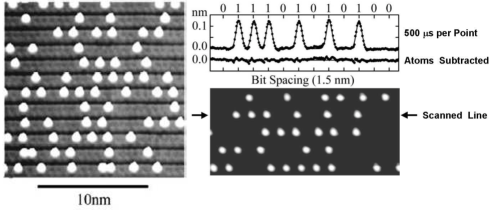
Storage of data in single atoms was demonstrated beautifully by Bennewitz et al. in 2002 Bennewitz2002 , who deposited silicon atoms from an STM tip onto a 52 reconstructed silicon-gold surface (Figure 8). Because of the nature of the reconstructed surface, every bit is stored into an area of 20 surface atoms, resulting in a density of . The method used by Bennewitz is a write-once technique, but one can also envision deposition of atoms from the gas phase, using, for instance, hydrogen (H) or chlorine (Cl) Bauschlicher2001 ; Rosi2001 .
III Positioning systems
A nanopositioner controls the position of an object with an accuracy on the order of nanometers. A probe data-storage system requires a miniature 2D nanopositioner, referred to as ‘the scanner’, to move the storage medium relative to the probe array. To be able to fully address the medium area, the displacement range must be equal to or larger than the distance between the probe tips in the probe array. This range, which is on the order of (see Section IV), must be combined with an accuracy on the order of a few nanometers. The access time of a probe data-storage system is mainly determined by the positioning system. The moving mass, the suspension spring stiffness, and the maximum actuator force determine this access time. The mechanical rigidity of the scanner puts a lower bound on the moving mass. The spring suspension must be sufficiently stiff to prevent undesired resonances and to provide shock resistance and vibration rejection. The actuator force should therefore be as large as possible, or at least on the order of millinewtons.
Several actuator types have been used for nanopositioner designs, such as piezoelectric, electromagnetic, electrostatic (e.g., comb drive and ‘inchworm’†††“An inchworm moves by gripping a surface with its hind legs while retracting its body”, Hubbard et al. Hubbard2006 .), electrothermal, and electrochemical actuators Hubbard2006 . The size of a probe data-storage device is an important constraint, severely restricting the space available for the nanopositioner. The actuators and scanner mechanics are commonly fabricated using microelectromechanical systems (MEMS) technology. The comparison of MEMS actuators by Bell et al. provides insight into which actuator types are most appropriate for a probe data-storage device Bell2005 . There are several suitable MEMS actuator types, whose displacement range is on the order of with nanometer resolution and whose maximum force is on the order of millinewtons. Electromagnetic, electrostatic (comb drive, dipole surface drive, inchworm), thermal, and piezoelectric actuators all seem promising candidates for use in a probe data-storage system, and scanner designs have been published for all these actuator types except for electrothermal actuators. A probable reason for the absence of thermally actuated scanners for probe data-storage is the high power required for fast thermal actuators.
Operating the scanner in closed-loop control is necessary to obtain nanometer positioning precision and adequate shock resistance Devasia2007 . The position sensors should have a large dynamic range; namely, nanometer accuracy over a 100- displacement range. Suitable position sensors have a small footprint and are based on a varying thermal conductance Lantz2005 ; Krijnen2011jmm ; Zhu2011thermcap ; Fowler2013 ; Mohammadi2014 , on a varying capacitance Chu2003 ; Lee2009 ; Pang2009 ; Huang2010 ; Zhu2011thermcap , on the position-dependent field of a permanent magnet Kartik2012 ; Tuma2014GMR , or on the piezoelectric effect Messenger2009 ; Bazaei2014 . Dedicated servo-pattern fields can enhance the positioning precision by providing a medium-derived position-error signal Eleftheriou2003 ; Pantazi2007 ; Sebastian2008nanopos ; Sebastian2012nanopos .
III.1 Electrodynamic actuation
Electromagnetic scanners use a coil to generate a magnetic field that leads to a force. All electromagnetic actuators designed for probe storage reported in the literature use a permanent magnet and a coil. An electromagnetic comb-drive actuator without permanent magnet has been constructed Schonhardt2008 , but has not been used in a scanner design yet. To distinguish electromagnetic actuators without and with permanent magnets, actuators with permanent magnets are referred to as electrodynamic actuators.
An advantage of electrodynamic scanners is the relatively straightforward linear actuator design (linear displacement-vs.-current curve), which simplifies controller design. Another advantage for mobile probe storage is that an electrodynamic scanner can operate at the generally low voltage available because it is current driven. A disadvantage is that permanent magnets are needed. Assembling an electrodynamic scanner is therefore more complicated than assembling, for instance, an electrostatic comb-drive scanner. It also means that it is difficult to make the scanner very thin. The energy consumption of electromagnetic scanners in general is relatively large because of the large currents required and the series resistance of the coils Engelen2013energy .
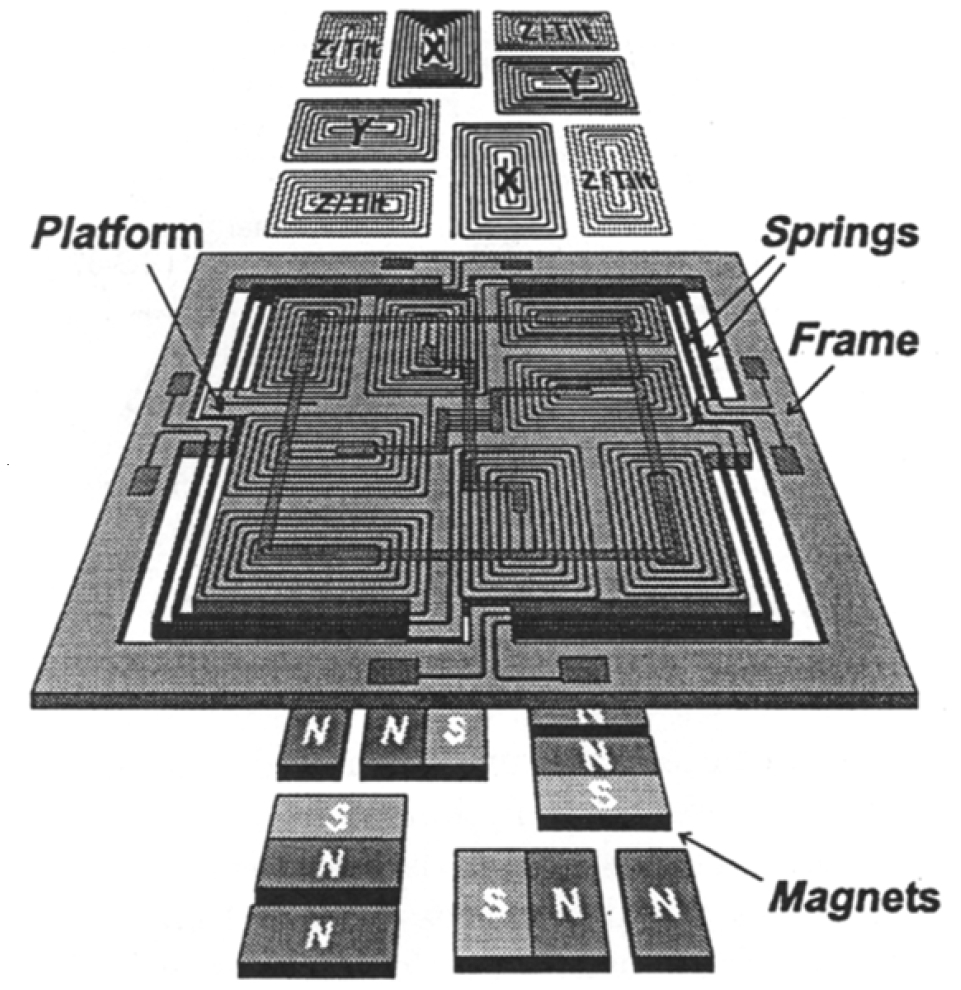
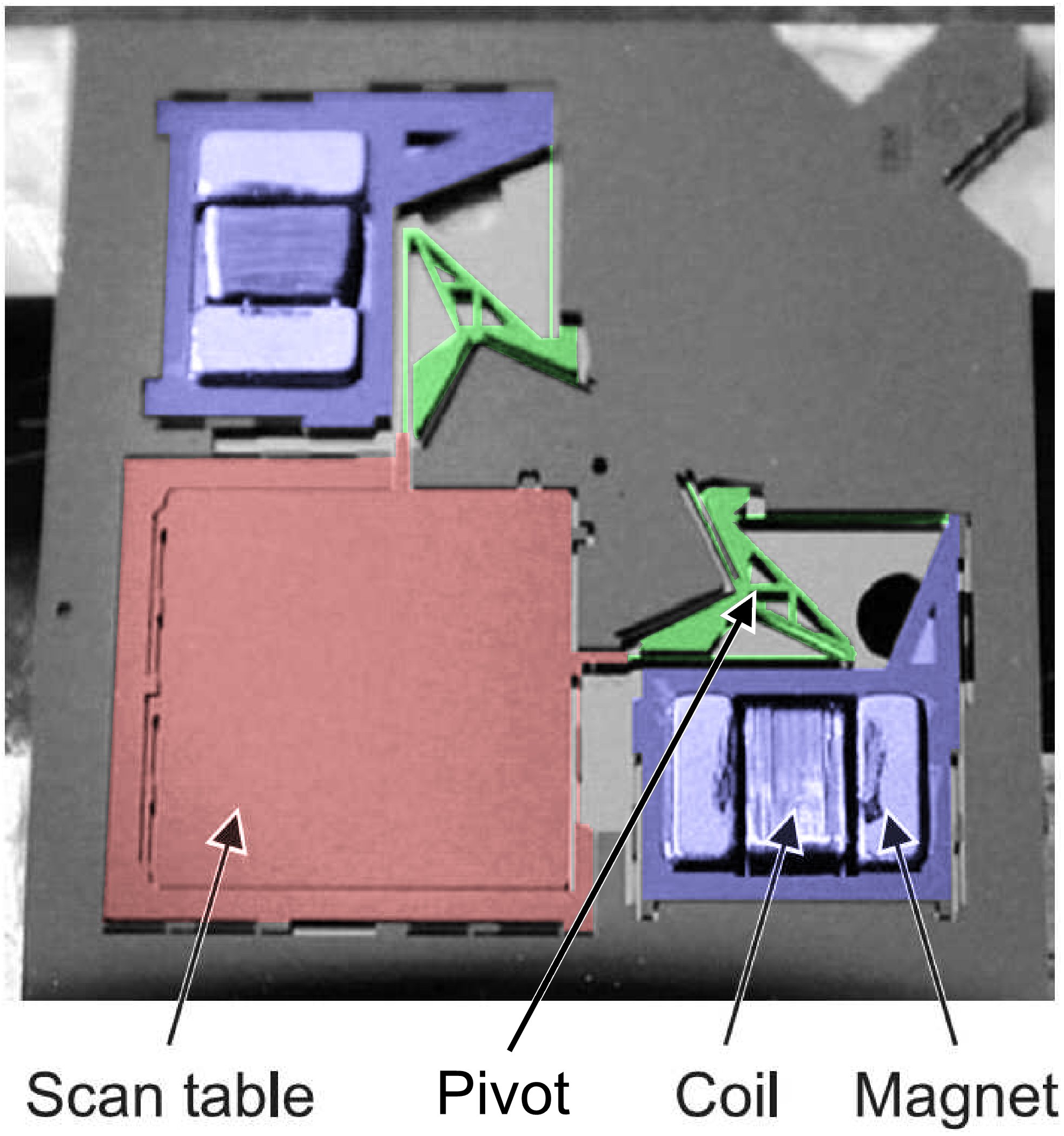
In 2000, Rothuizen et al. from IBM reported their proof-of-concept electrodynamic scanner for probe data storage (see Figure 9): a five degrees of freedom // scanner, including tilt about the - and -axes, fabricated from silicon and electroplated copper springs and coils. The scanner contains a moving platform held in a outer frame Rothuizen2000 . The displacement range is ; however the required power of about is very high. An improved design was reported two years later Rothuizen2002 , fabricated from a 200--thick SU-8 layer, which uses a similar configuration for the coil and magnet. It improves on power dissipation ( at displacement), fabrication cost, and compactness by placing the spring system below the moving platform. Two years later, a radical change in design was reported (Pantazi2004, ; Lantz2007, , see Figure 10). This new design is fabricated from a 400--thick silicon wafer by deep reactive-ion etching through the full thickness of the wafer, i.e., the design is an extrusion of a two-dimensional layout. It features a mass-balancing concept to render the system stiff against external shocks while keeping it compliant for actuation such that the power dissipation is low. The actuator and scan-table masses are linked via a rotation point, enforcing their movement in mutually opposite directions: when the actuator moves up, the table moves down and visa versa. External shocks exert inertial forces on the actuator and scan-table mass, but, because the directions of the inertial forces are equal, they cancel each other through the rotation point. Because the springs are high (wafer thickness), the stiffness in the -direction is large for passive shock rejection. Coils and magnets are glued manually onto the device. The actuator generates a force of . Its power usage at displacement is ( current); this has been improved to about ( current) ‡‡‡Private communication with Mark A. Lantz, IBM Research – Zurich.. The medium sled is , while the complete device is ; the areal efficiency is about 25% and has decreased dramatically in comparison to the earlier designs. The in-plane resonance frequencies lie around ; the first out-of-plane resonance frequency lies an order of magnitude higher.
Another electrodynamic scanner was reported in 2001 by Choi et al. from Samsung Choi2001a ; Choi2001b , see Figure 11. That scanner is fabricated from silicon; the coils are made by filling high-aspect-ratio silicon trenches. The medium sled size is . The displacement of at is smaller than that achieved by the scanner by IBM; however, the displacement was measured without the top magnets and yokes that were planned in the design to increase the magnetic field and force. The measured in-plane resonances are (translational) and (rotational).
A plastic electrodynamic scanner has been developed by Seagate Huang2009 ; however, little design and fabrication information is available. The scanner has three degrees of freedom: / translation and rotation about the -axis. The displacement range is large, but the resonance frequency is only .
III.2 Electrostatic comb-drive actuation
Electrostatic comb drives Tang1989 are microelectromechanical actuators that are often used in MEMS technology, because their design and fabrication are relatively straightforward. A comb drive consists of two interdigitated structures, shaped like combs, that attract each other when they are charged oppositely by application of an external voltage. The force generated, however, is small, and many fingers are needed to generate sufficient force, reducing the areal efficiency. Other electrostatic actuators, such as the dipole surface drive and the shuffle drive (see Section III.3), can generate more force, but are more complicated to manufacture and to control. The force generated is proportional to and in the direction of increasing capacitance; the combs attract each other because the increase in overlap between the comb fingers increases the capacitance Johnson1995a . The capacitance is a function of the spacing (the gap) between fingers, and there is a sideways force on a finger if the finger is not exactly centered between the two opposing fingers. Therefore, the spring suspension must restrict motion in the transverse direction to prevent this ‘side snap-in’. A comb drive’s force is proportional to the square of the applied voltage. Because of this quadratic dependence, the polarity of the applied voltage is unimportant, and the force is always attractive. To move a stage in both positive and negative direction, two or more comb-drive actuators are required. Because the spring suspension force depends linearly on the position, the displacement depends quadratically on the applied voltage. This relation can be linearised by driving the comb drives in differential mode, reducing the force of one comb drive by simultaneously applying a voltage on the comb drive pulling in the opposite direction Grade2004 .
The maximum force of a comb-drive actuator depends on the maximum available voltage, if not the breakdown voltage, across the finger gap. The breakdown voltage of comb drives is above for common micrometer-sized gaps Chen2006 , and is usually higher than the available voltage. To increase the maximum voltage, DC/DC step-up conversion is used. Examples of DC/DC converters specifically designed for MEMS applications are a high-voltage-CMOS design that converts voltages from to using an external coil Saheb2007 , and a standard CMOS design that is capable of converting to without external components Hong2003 .
Compared with electromagnetic actuators, an advantage of comb-drive actuators is their ease of fabrication. Moreover, their energy consumption is lower, but for a fair comparison with other scanners, also the energy consumption of the driving (DC/DC conversion) circuitry must be taken into account. Although a comb drive is a non-linear actuator, driving one is much simpler than driving the electrostatic stepper motors discussed below. A comb-drive actuator can simultaneously be used as a position sensor by measuring the capacitance which changes as a function of position Chu2003 ; Pang2009 ; Huang2010 . The capacitance is measured electrically, and the frequency of the measurement voltage is chosen well above the mechanical resonance frequencies to not interfere with the actuation. Disadvantages include the generally high voltage required and the low areal efficiency because of the large area needed for comb fingers to generate sufficient force. The force output highly depends on the minimum gap size that can be fabricated; reduced gap sizes achieved with improved fabrication methods will result in stronger comb-drive actuators. In practice, the maximum force and voltage are limited by side pull-in because of insufficient spring suspension stiffness Zhang2014pullin . When the spring suspension is not sufficiently stiff in the in-plane direction perpendicular to the direction of travel, the moving part of the comb drive may snap sideways against the stationary part, generally resulting in terminal failure of the device. Several suspension designs have been published that improve on the common folded-flexure design Tang1989 in order to specifically prevent snap-in while maintaining a large compliance in the desired travel direction Olfatnia2013 ; Krijnen2014 . However, these improved suspension designs substantially increase the footprint of the actuator, reducing their attractiveness for use in a high-density data storage device. Note that these suspension designs are not restricted to comb drives and can also be used for the other actuator types.
Already in 1992, a nanopositioner with an integrated probe tip was described Yao1992 . It featured electrostatic parallel-plate (gap-closing) actuators, moving the probe instead of the ‘medium’. However, its displacement range of at is very limited. Another early design included position sensing and control, obtaining a displacement of at just Cheung1996 . However, the actuator is too thin to carry a load.
In 2000, Carley et al. from Carnegie Mellon University described a comb-drive scanner for probe storage that had originally been designed for a vibratory-rate gyroscope Carley2000 ; Carley2001 . The scanner reaches displacement at ; it contains 800 fingers in total, with height and gap. This design was improved using parametric optimization to optimize the footprint for stroke, keeping the topology fixed Alfaro2002 (see Figure 12). Although Figure 12 is not drawn to scale, it is indicative of the generally low areal efficiency of comb-drive scanners.
The comb-drive scanner reported by Kim et al. uses 27,552 3--thick fingers with height and gap Kim2003 (see Figure 13). These dimensions are common for comb-drive designs, where the maximum aspect ratio (height-to-gap ratio) is limited to approx. 20:1 by the deep reactive-ion etching fabrication process Jansen2009abrev . The scan table is large, and static displacement is reached at . Because of the large number of fingers, the force is large and the required voltage is low; however, this also leads to a low areal efficiency of approximately 11%.
Kwon et al. published an /-scanner for optical applications Kwon2006 , but the design could also be applied to probe storage. The design uses ‘L’-shaped suspension springs and rotational comb drives (see Figure 14). Its displacement range is at ; however it is unclear whether the suspension is stiff enough for use in probe storage.
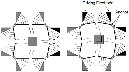
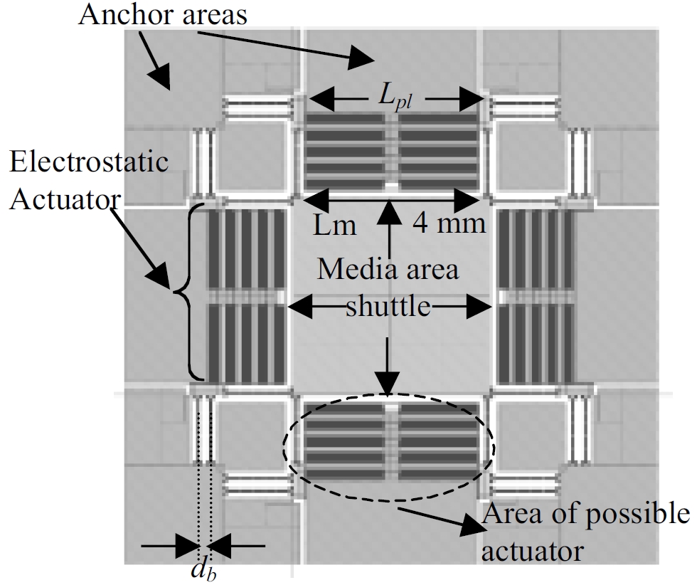
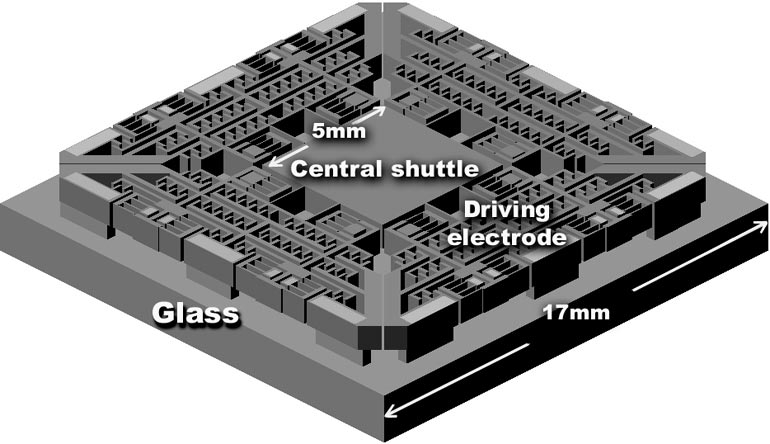
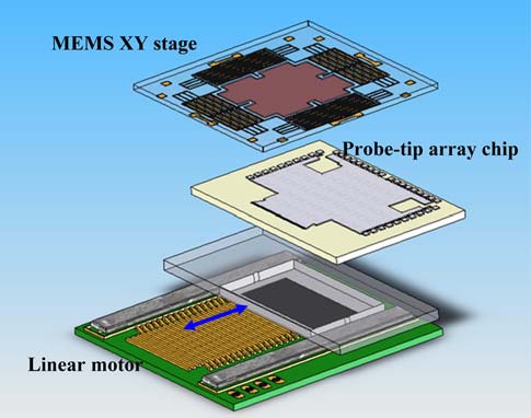
The somewhat unconventional positioning system design by the Data Storage Institute in Singapore features an electrostatic comb-drive /-scanner Lu2005 for precise positioning and a 1D miniature electromagnetic linear motor for coarse positioning of a 1D probe array Yang2007 ; Pang2009 (see Figure 15). By using an extra coarse positioner, a small number of probes in a 1D array can be used instead of a 2D probe array. The comb-drive scanner features a scan table of ; the areal efficiency is 36%. Simulations indicate a static displacement of at , but no measurement results are reported.
All comb-drive scanners mentioned above directly link the actuators to the scan table. This means that in-plane shocks have to be compensated actively for by the actuators. Especially at large displacements, when the available force is low, this leads to a low shock-rejection capability. The shape of the comb-drive fingers may be tailored to increase the available force and to provide improved shock rejection Engelen2009 ; Engelen2010optim . The electrostatic scanner designs by Sasaki et al. use mass balancing for internal shock force rejection Sasaki2008 . Inertial forces due to fast acceleration in the -direction may influence the comb finger gap in the -direction, which may lead to instability in the comb drives for the -direction. To cancel these inertia forces in the -direction, the scan table is split into two plates of equal mass that are actuated in mutually opposite directions. External inertial forces are not cancelled as opposite movement is not mechanically enforced. The best of the three designs investigated reached static displacements of at and at for the - and -directions, respectively Sasaki2008 .
A very direct comparison between comb drives and electrodynamic actuation is the retrofitting of IBM’s mass-balanced scanner Pantazi2004 ; Lantz2007 with electrostatic comb drives Engelen2008 . The comb-drive scanner uses tapered comb-drive fingers, obtaining displacement ranges of at and at in the - and -directions, respectively. The resonance frequencies in both directions (around ) are slightly lower than those of the electrodynamic scanner. The total area of the scanner is larger in both directions than the total area of the electrodynamic scanner. However, because no permanent magnets are needed, the comb-drive version can be made thinner than the electrodynamic scanner.
III.3 Electrostatic stepper motors
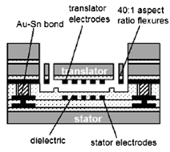
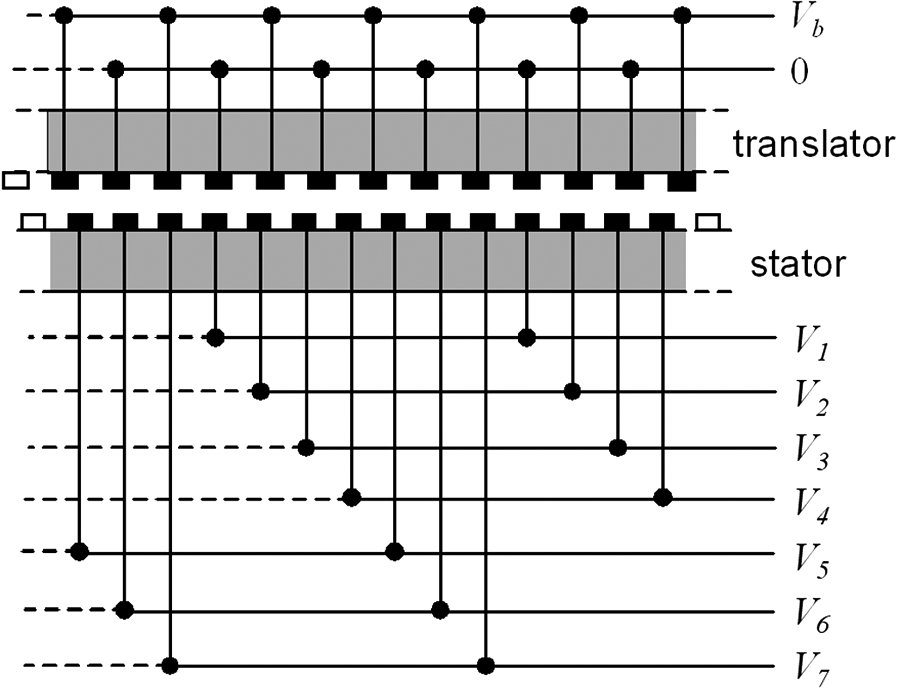
Figure 16 shows the electrostatic dipole surface drive of Agilent Hoen2003 ; Agarwal2006 . The translator features a periodic pattern of electrodes and is suspended above the stator, which also has a periodic pattern of electrodes but with a different pitch. Oppositely charged translator and stator electrodes will try to align with each other, increasing the capacitance between them, and creating a translational force. Sequentially applying a voltage on , , …, , Figure 16, results in a stepping motion of the translator to the left. The step size of is determined by the difference in electrode pitch between stator and translator. Smaller displacements are made by adjusting the voltage on one of the electrodes. In the design reported by Agarwal et al. Agarwal2006 , the gap between the stator and translator electrodes is . A high out-of-plane to in-plane stiffness ratio is required, because the available force is limited by the vertical snap-in voltage ( in this case). A displacement of was reached with bias; larger displacements of up to were reached, but in that case significant out-of-plane motion was observed Agarwal2006 . The out-of-plane force can be cancelled by another dipole surface drive placed ‘upside-down’ on top of the translator.
The dipole surface drive can potentially provide a large force at low voltages, because the capacitance (and thus the force) between translator and stator electrodes can be made large owing to the small gap size that is not limited by lithography or deep reactive-ion etching. Because the actuator is placed under the scan table, the areal efficiency is greatly increased compared with, e.g., comb-drive designs. However, the fabrication process and drive circuitry are more complex than for electromagnetic actuators and electrostatic comb drives. To make the design more shock-resistant, perhaps a 2D mass-balancing scheme could be used similar to IBM’s electrodynamic scanner Lantz2007 without decreasing the areal efficiency.
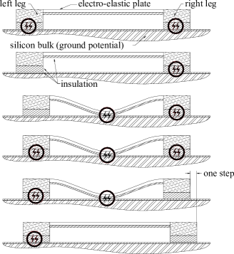
Another electrostatic stepper motor is the ‘inchworm’ shuffle drive by Tas et al. Tas1998 from the University of Twente. The shuffle drive consists of two clamp ‘feet’ connected by a thin plate. The feet and plate can be pulled towards the bulk individually. Figure 17 shows how the motor makes a step. The actuator’s output force and step size are determined by how much plate deformation is obtained when applying a voltage on the plate. The step size is on the order of tens of nanometers, but highly depends on the displacement because of the restoring force of the spring suspension Patrascu2007b . The force generated is large, because the capacitance change of the parallel-plate gap-closing actuator is relatively large and because the plate acts as a mechanical lever. Sarajlic et al. describe a shuffle motor with a displacement range and an output force of at driving voltages of and for the plate and clamps, respectively Sarajlic2005d . A 2D shuffle motor reached displacements of (corresponding to force) at driving voltages of and for the plate and clamps, respectively, being limited only by the design layout Sarajlic2005a . Unfortunately, stiction and friction of the feet are a large problem for reliable operation Patrascu2006 . Moreover, a complex control loop is required Patrascu2007b . Interestingly, because the device is electrostatically clamped to the base plate, it is inherently shock-resistant, but when the shock force plus the spring force exceed the stiction force, there is no way to compensate for them.
III.4 Piezoelectric actuation
Piezoelectric actuation is commonly used for scanning probe microscopy, where there is ample space for the actuator. Piezoelectric materials deform when a voltage is applied, resulting in a translational, rotational, or bending motion. Piezoelectric elements need to be quite large to provide the required displacement range for probe storage Muralt2000 . Fortunately because the generated force is large, mechanical stroke amplification can be used to increase the displacement range of small piezoelectric elements. Commonly required voltages are comparable to the voltages required for electrostatic actuators.
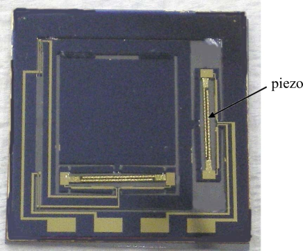
Several scanner designs using PZT actuators and stroke amplification are described by Zhang et al. Zhang2003 . An improved design reached at an applied voltage of Faizul2009b . That scanner consists of a silicon MEMS displacement stage to which PZT actuators have been attached manually (see Figure 18). The scan table is in size. Although the fabrication of a micromachined stacked PZT actuator especially designed for the scanner is discussed, only measurements using larger commercial PZT actuators are shown Faizul2009b . The PZT actuators generate large forces () and their small displacement is mechanically amplified 20 times to move the scan table. The maximum force of on the scan table is more than an order of magnitude larger than those of the scanners discussed above. The displacement versus voltage measurements show hysteresis, but this can be reduced by using charge control instead of voltage control Comstock1981 . It will be interesting to see whether the stiff suspension provides a passive shock-resistance comparable to the shock resistance of IBM’s mass-balanced electrodynamic scanner. The fabrication complexity of attaching the PZT actuators on the silicon stage is comparable to the glueing of permanent magnets onto IBM’s electrodynamic scanner shown in Figure 10.
IV Probe arrays and parallel readout
Although the probes used in probe-based data storage are originally derived from standard AFM and STM probes, they have become very complex over time. Not only do the probes require electrical actuation and readout, they also have to be extremely wear resistant and have to fit into a restricted area. Another challenging task is to realize probe arrays with thousands of tips in parallel. Readout of these arrays is far from trivial, especially as the number of probes increases.
IV.1 Probe technology and arrays
The most advanced probe arrays have been realized by the IBM–Research Zurich probe-storage team. Already in 1999, Lutwyche et al. realized a 55 array of probes with tip heaters and piezoresistive deflection readout Lutwyche1999 . Ultrasharp tips were obtained by oxidation sharpening of isotropically etched tips. The tips were located at the end of cantilevers that are bent towards the medium by purposely introducing stress gradients to clear the lever anchors from the medium. Boron implantation in specific regions of Si cantilevers was used to define piezoresistors and tip heaters. To increase the sensitivity up to a / of , where is the resistance, constrictions were introduced at the base of the cantilever, but these constrictions led to higher resistance, increasing the pink noise.
In the subsequent 3232 array, piezoresistive sensing was abandoned Despont2000 . In this array, the cell size was reduced from to , while keeping the cantilever spring constant at with a resonance frequency of . The array size was 3 mm 3 mm, and thermal expansion deteriorating the tip alignment became an issue. Integrated heaters were positioned in the array to keep temperature variations within over the chip. The array worked remarkably well: of the cantilevers worked Lutwyche2000 and a density of at net data rate was shown Durig2000 .
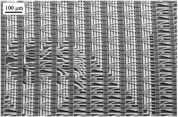
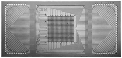
An impressively tight integration of the probe array with CMOS was demonstrated by Despont et al. Despont2004 . In this method only the integrated cantilevers are transferred to the CMOS chip, and the MEMS carrier wafer is first ground and then etched away. On , as many as 300 electrical copper interconnects of were realized. An array of 4096 probes with outer dimensions of 6.4 mm 6.4 mm was constructed (Figure 19), and the interconnects had a yield of .
As tip wear can be reduced by applying less force to the tip, the probe design was modified so that the spring constant reduced to . As a result, the probe applies very little force to the tip during read actions. During write actions, this force can be electrostatically increased up to by means of a capacitive platform at a potential of .
The work of IBM triggered the interest of other companies. For heated tip writing on piezoelectric and phase-change media, researchers at LG Electronics in Korea built a small array of thermal probes Lee2002a . Heater platforms were integrated into boron-doped silicon by creating a constriction at the cantilever end and covering the cantilever legs with gold. Conductive tungsten tips were grown by focused ion-beam deposition. In the next generation, readout was added by integrating piezoelectric PZT layers on the cantilever legs Lee2003 . Feature heights of could easily be distinguished. The array was extended to a size of 128128 probes, and the sensitivity improved to Nam2007 . A wafer-transfer method was developed for a 3434 array Kim2006 ; Kim2007 , very much along the lines of the IBM process. Rather than silicon, -nm-thick silicon nitride probes were used with integrated polysilicon heaters. The spring constant was still relatively high (). Sharp tips were realized by KOH etching of pits into the silicon wafer and subsequent filling of the pits with silicon nitride, enabling bit dimensions of .
At the University of Twente, cantilever arrays with small variations in tip-sample distance were fabricated Koelmans2011a . As tip wear increases with load force, it is important that the tip-sample distance is similar for each tip in an array. The well-known KOH etching process for single tips, reported in Albrecht1990 , was extended to arrays of cantilevers that feature self-aligned tips. The simple and easily scalable fabrication method was demonstrated in an array of 10 tips that showed a standard error of in tip-sample spacing Koelmans2011a .
Researchers at the Shanghai Institute of Microsystems and Information Technology have realized a small cantilever array, with integrated heater tips and piezoelectric deflection detection Yang2006 . These arrays have been used to characterize the wear of polymer recording media as a function of tip temperature and radius Bao2008 .
At the Data Storage Institute in Singapore, Chong et al. realized 201 and 152 arrays, using a fabrication technique along the lines of the early IBM work Chong2005 . The scanning concept, however, is different, and features a large stroke actuator in one direction. The total storage area can thus be much larger than the size of the array Yang2007 . The --long and --thick cantilevers of the array had a spring constant of and a resonance frequency of . The tip radius was rather large (), resulting in bit dimensions on the order of . Cooling times of were measured by monitoring the heater platform temperature with an infrared camera.
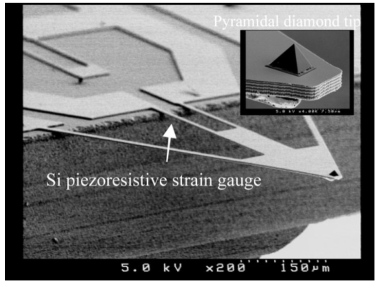
Researchers at Pioneer and at the Tohoku University in Japan investigated arrays of probes with diamond tips and integrated piezoresistive sensors for ferroelectric data storage Takahashi2006a , see Fig. 20. The boron-implanted Si piezoresistive Wheatstone bridge was very sensitive, with a / of Takahashi2006 . In contrast, the diamond probes had a relatively poor radius of curvature. Attempts were made to replace the diamond tips by metal versions, and it was demonstrated that Ruthenium tips perform relatively well Takahashi2007 .
IV.2 Parallel operation
The massive parallelism of the probe arrays, which is prerequisite for obtaining data rates comparable to those of magnetic hard-disk heads, poses a large challenge in probe-based data storage. Several thousands of probes have to be addressed simultaneously. The main functions of each probe are positioning, reading and writing. Positioning, as described in section III, is in most cases done by moving the complete array or the storage medium in plane and parallel to the probe array, simplifying the task of each probe.
Scanning the medium has two distinct advantages over scanning the probes. To obtain desired read and write speeds, arrays have to scan at considerable rate, thereby inducing high-frequency vibrations that create unwanted cantilever movement. Preventing the occurrence of these vibrations is a major additional challenge for any control loop. Secondly, electrical connections to the probes can be realized more easily, because the probes do not move with respect to the read-channel electronics. Researchers at the Data Storage Institute presented a solution where the coarse-positioning stage has a flexible wire to the readout electronics, although also in this design the fine positioning is directly connected to the cantilever array Yang2007 .
Movement in the -direction, where is defined as the direction normal to the medium, can be done on a per-array basis instead of on a per-probe basis. This hugely simplifies the control required to operate an array of thousands of probes. However, the fabrication tolerances of the array and the medium have to be such that every probe in the array is in the appropriate tip-medium distance range. Too large a tip-sample separation results in a failure when an attempt to write or read a bit is done. The other extreme leads to a probe that is pushed into the medium with considerable force (depending on the spring constant of the cantilever), leading to excessive tip wear. Without independent -motion, these demands on the medium and probe array increase tremendously. The technically most mature probe-storage system, described in Pantazi2008 , is based on thermomechanical storage and features a 6464 cantilever array, of which are active. By determining the electrostatic pull-in voltage for each cantilever, the initial tip-sample separation is calculated to have a standard deviation of . With a cantilever spring constant of , this would lead to an additional loading force of hundreds of nN.
The read and write operations require the independent addressing of each probe. Traditionally, AFM probes are monitored by an optical readout system, mainly based on the optical beam-deflection technique Meyer1988 ; Meyer1988er . Although optical readout has been demonstrated for arrays of cantilevers Lang1998 ; Sulchek2001 ; Alvarez2005 ; Koelmans2010 ; Koelmans2011thesis ; Pjetri2011 ; Honschoten2011 none of the readout schemes has been implemented in probe storage. Optical readout alone, however, would not suffice. The probes have to be actuated for the write operation. Wired schemes are implemented to achieve this. Wireless schemes and passing signals through the storage medium have been proposed Abelmann2003 , but not yet realized.
Wiring solutions are based on a time-multiplexing scheme to address the array row by row Despont2000 ; Kim2007 , as is usually done in DRAM. With a growing number of probes, the maximum current passed through a row or signal line increases. For higher numbers of probes, an electrically stable wiring material, capable of carrying high current densities and also having a low resistivity, must be used. As shown in Figure 21, Despont and co-workers have used two-level wiring of both gold and nickel in the 3232 array Despont2000 . Schottky diodes formed by doped silicon/nickel interfaces were introduced to avoid crosstalk between probes.
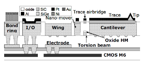
In the 6464 array reported in Despont2004 , the number of connections has increased to three per probe. In this case, a second wafer with the CMOS circuitry is used to which the probes are bonded, as done in Kim2007 . An alternative integration with CMOS is the single-wafer process described in Severi2009 . Here first the CMOS circuitry is created, and on the last metalization layer, a chemical mechanical polishing (CMP) step is performed. Next an insulating layer of -nm-thick silicon carbide and a sacrificial oxide layer of are deposited. A structural silicon germanium layer of is later deposited to allow definition of the cantilevers. Then the cantilevers are etched and the sacrificial oxide is removed to allow cantilever actuation, see Figure 22.
V Final remarks
Probe-based data storage has been a very active area of research, leading to a prototype demonstration in 2005 using topographic storage. Topographic probe-storage is the most mature probe-storage technology. Very high densities of , have been achieved in combination with excellent retention, endurance, and read and write speeds.
Phase-change probe storage is severely limited by the difficulty of amorphizing crystalline regions of the storage medium. Most of the work on phase-change probe storage has been discontinued, and the results feed into the currently ongoing realization of solid-state phase-change memory cells. Probes have successfully demonstrated the scalability of phase-change memory and allow rapid nanoscale characterization.
Magnetic probe storage was jump-started by hard-disk research, leading to many demonstrations of and insights into the switching of bit-patterned media, which are currently an active topic of research in the hard-disk industry. Demonstrations are limited to a density of a few . Such densities give rise to the question whether magnetic probe storage should be pursued any further.
Ferroelectric storage shows promising densities, read speeds and endurance numbers, and has attracted the interest of academia and industry.
The research into probe storage has led to huge contributions to probe and array technologies, medium development, positioning, and sensory and control systems for the nanometer scale. In probe and array technology, much work was done scale up the single probe used in scanning probe microscopy to an array of probes reading and writing data. Wear of probe and media have been greatly reduced. The most prominent positioning systems are MEMS scanners using electrodynamic (using a coil and a permanent magnet) or electrostatic comb-drive actuators, achieving sub-nanometer positioning accuracy. The mature positioning system of the 2005 prototype demonstration uses electrodynamic actuators with a mechanical design for shock-resistance, bringing it closer to productization. Probe-storage research has strongly impacted and contributed to a variety of other application areas, e.g., probe-based nanolithography, probe-based nanofabrication, 3D probe patterning and fast nano-scale imaging.
No commercial probe-storage product exists as of today. One of the reasons that major efforts by industry to develop a probe-storage system have stopped is the accelerated introduction of Flash memory, driven by the introduction of the digital cameras and the USB memory stick.
Mechanically addressed storage does offer a cost advantage over lithographically-defined storage. For mechanically-addressed storage, the relatively large cost of the initial system dominates the total device cost, whereas the media cost is relatively low. In contrast, electrically-addressed storage has little initial overhead cost, and the total cost is dominated by the capacity. Therefore, scaling to more media per device (adding platters in an HDD) or using exchangable media (tape storage) is significantly more cost-effective than increasing the die area of a Flash memory chip. This is why the magnetic hard-disk remains the nonvolatile storage system of choice for data centers in terms of capacity, and why tape storage is a thriving industry for data storage at even larger capacities. For a probe-based storage device, we envision a cost structure similar to that of the other mechanically-addressed storage devices. Moreover, mechanically-addressed storage systems are much less dependent on the lithographic capabilities to scale the data density, e.g., chemical etching techniques are used to reach the probe dimension required and the probe, in turn, creates very high data densities on a relatively cheap medium.
Current commercial storage technologies have reached such scale that the cost has been reduced to a point where other performance characteristics besides the areal density, such as low access time, high readback data rate, and small form factor, strongly influence the choice of technology. However, to reach atomic densities or atomic nano-manipulation capability, the probe-based approach is clearly the best suited and most mature technology.
The authors hope this review will provide future researchers a quick and comprehensive insight into the amazing achievements in probe-based data storage that paved the way for future nanotechnology research and applications.
Acknowledgments
We gratefully acknowledge our (former) colleagues in the SPAM team at the University of Twente for the many stimulating discussions that laid the basis for this work. We thank M. Gemelli, M. Khatib and O. Zaboronski for discussion and valuable input. We also thank C. Bolliger and M. Lantz for proofreading the manuscript, A. Sebastian, H. Bhaskaran and D. Wright for fruitful discussions and E. Eleftheriou for his support of this work.
References
- (1) M. Lutwyche, C. Andreoli, G. Binnig, J. Brugger, U. Drechsler, W. Häberle, H. Rohrer, H. Rothuizen, P. Vettiger, G. Yaralioglu, C. Quate, 2D AFM cantilever arrays a first step towards a terabit storage device, Sens. Actuators A 73 (1-2) (1999) 89–94. doi:10.1016/S0924-4247(98)00259-3.
- (2) Y. Zhao, E. Johns, M. Forrester, A MEMS read-write head for ferroelectric probe storage, in: Proc. MEMS 2008, Tucson, AZ, USA, 2008, pp. 152–5. doi:10.1109/MEMSYS.2008.4443615.
- (3) Y. Hiranaga, T. Uda, Y. Kurihashi, H. Tochishita, M. Kadota, Y. Cho, Nanodomain formation on ferroelectrics and development of hard-disk-drive-type ferroelectric data storage devices, Jpn. J. Appl. Phys. 48 (9 Part 2) (2009) 09KA18–1–5. doi:10.1143/JJAP.48.09KA18.
- (4) H. F. Hamann, M. O’Boyle, Y. C. Martin, M. Rooks, H. K. Wickramasinghe, Ultra-high-density phase-change storage and memory, Nat. Mater. 5 (5) (2006) 383–387. doi:10.1038/nmat1627.
- (5) P. Kappenberger, F. Luo, L. J. Heyderman, H. H. Solak, C. Padeste, C. Brombacher, D. Makarov, T. V. Ashworth, L. Philippe, H. J. Hug, M. Albrecht, Template-directed self-assembled magnetic nanostructures for probe recording, Appl. Phys. Lett. 95 (2) (2009) 023116. doi:10.1063/1.3176937.
- (6) D. Wiesmann, C. Rawlings, R. Vecchione, F. Porro, B. Gotsmann, A. Knoll, D. Pires, U. Duerig, Multi Tbit/in2 storage densities with thermomechanical probes, Nano Lett. 9 (9) (2009) 3171–3176. doi:10.1021/nl9013666.
- (7) K. Tanaka, Y. Cho, Actual information storage with a recording density of 4 Tbit/in2 in a ferroelectric recording medium, Appl. Phys. Lett. 97 (9) (2010) 092901. doi:10.1063/1.3463470.
- (8) C. D. Wright, M. Armand, M. M. Aziz, Terabit-per-square-inch data storage using phase-change media and scanning electrical nanoprobes, IEEE Trans. Nanotechnol. 5 (1) (2006) 50–61. doi:10.1109/TNANO.2005.861400.
- (9) M. H. Kryder, E. C. Gage, T. W. Mcdaniel, W. A. Challener, R. E. Rottmayer, G. Ju, Y. T. Hsia, M. F. Erden, Heat assisted magnetic recording, Proc. IEEE 96 (11) (2008) 1810–1835. doi:10.1109/JPROC.2008.2004315.
- (10) Y. Cho, S. Hashimoto, N. Odagawa, K. Tanaka, Y. Hiranaga, Realization of 10 Tbit/in2 memory density and subnanosecond domain switching time in ferroelectric data storage, Appl. Phys. Lett. 87 (23) (2005) 232907–1. doi:10.1063/1.2140894.
- (11) T. Onoue, H. Siekman, L. Abelmann, J. C. Lodder, Heat-assisted magnetic probe recording onto a thin film with perpendicular magnetic anisotropy, J. Appl. Phys. D 41 (15) (2008) 155008. doi:10.1088/0022-3727/41/15/155008.
- (12) A. Sebastian, D. Wiesmann, P. Baechtold, H. Rothuizen, M. Despont, U. Drechsler, Feedback enhanced thermo-electric topography sensing, in: Proc. 15th Int. Conf. on Solid-State Sensors, Actuators and Microsystems (Transducers ’09), Denver, CO, 2009, pp. 1963–1966. doi:10.1109/SENSOR.2009.5285675.
- (13) R. J. Cannara, B. Gotsmann, A. Knoll, U. Dürig, Thermo-mechanical probe storage at Mbps single-probe data rates and Tbit in-2 densities, Nanotechnol. 19 (39) (2008) 395305. doi:10.1088/0957-4484/19/39/395305.
- (14) Y. Cho, S. Hashimoto, N. Odagawa, K. Tanaka, Y. Hiranaga, Nanodomain manipulation for ultrahigh density ferroelectric data storage, Nanotechnol. 17 (7) (2006) S137–S141. doi:10.1088/0957-4484/17/7/S06.
- (15) H. Bhaskaran, A. Sebastian, U. Drechsler, M. Despont, Encapsulated tips for reliable nanoscale conduction in scanning probe technologies, Nanotechnol. 20 (10) (2009) 105701. doi:10.1088/0957-4484/20/10/105701.
- (16) M. A. Lantz, D. Wiesmann, B. Gotsmann, Dynamic superlubricity and the elimination of wear on the nanoscale, Nat. Nanotechnol. 4 (9) (2009) 586–591. doi:10.1038/nnano.2009.199.
- (17) N. Tayebi, Y. Zhang, R. J. Chen, Q. Tran, R. Chen, Y. Nishi, Q. Ma, V. Rao, An ultraclean tip-wear reduction scheme for ultrahigh density scanning probe-based data storage, ACS Nano 4 (10) (2010) 5713–5720. doi:10.1021/nn1013512.
- (18) J. Yang, MEMS-based probe recording technology, J. Nanosci. Nanotechnol. 7 (1) (2007) 181–192. doi:10.1166/jnn.2007.015.
- (19) C. D. Wright, M. M. Aziz, P. Shah, L. Wang, Scanning probe memories – technology and applications, Curr. Appl. Phys. 11 (2, Supplement) (2011) e104–e109. doi:10.1016/j.cap.2010.11.130.
- (20) M. Gemelli, L. Abelmann, J. B. C. Engelen, M. G. Khatib, W. W. Koelmans, O. Zaboronski, Memory Mass Storage, Springer-Verlag, 2011, Ch. Probe storage, pp. 99–167.
- (21) R. Garcia, A. W. Knoll, E. Riedo, Advanced scanning probe lithography, Nat. Nanotechnol. 9 (8) (2014) 577–587. doi:10.1038/nnano.2014.157.
- (22) D. Pires, J. L. Hedrick, A. De Silva, J. Frommer, B. Gotsmann, H. Wolf, M. Despont, U. Duerig, A. W. Knoll, Nanoscale three-dimensional patterning of molecular resists by scanning probes, Science 328 (5979) (2010) 732–735. doi:10.1126/science.1187851.
- (23) P. Vettiger, M. Despont, U. Drechsler, U. Dürig, W. Häberle, M. I. Lutwyche, H. E. Rothuizen, R. Stutz, R. Widmer, G. K. Binnig, ‘Millipede’ - more than one thousand tips for future AFM data storage, IBM J. Res. Dev. 44 (3) (2000) 323–340. doi:10.1147/rd.443.0323.
- (24) A. Knoll, P. Bachtold, J. Bonan, G. Cherubini, M. Despont, U. Drechsler, U. Durig, B. Gotsmann, W. Haberle, C. Hagleitner, D. Jubin, M. A. Lantz, A. Pantazi, H. Pozidis, H. Rothuizen, A. Sebastian, R. Stutz, P. Vettiger, D. Wiesmann, E. S. Eleftheriou, Integrating nanotechnology into a working storage device, Microelectron. Eng. 83 (4-9 SPEC ISS) (2006) 1692–1697. doi:10.1016/j.mee.2006.01.206.
- (25) H. Pozidis, W. Häberle, D. Wiesmann, U. Drechsler, M. Despont, T. R. Albrecht, E. Eleftheriou, Demonstration of thermomechanical recording at 641 Gbit/in2, IEEE Trans. Magn. 40 (4) (2004) 2531–2536. doi:10.1109/TMAG.2004.830470.
- (26) H. J. Mamin, D. Rugar, Thermomechanical writing with an atomic force microscope tip, Appl. Phys. Lett. 61 (8) (1992) 1003–1005. doi:10.1063/1.108460.
- (27) W. P. King, T. W. Kenny, K. E. Goodson, G. Cross, M. Despont, U. Dürig, H. Rothuizen, G. K. Binnig, P. Vettiger, Atomic force microscope cantilevers for combined thermomechanical data writing and reading, Appl. Phys. Lett. 78 (9) (2001) 1300–1302. doi:10.1063/1.1351846.
- (28) U. Drechsler, N. Burer, M. Despont, U. Dürig, B. Gotsmann, F. Robin, P. Vettiger, Cantilevers with nano-heaters for thermomechanical storage application, Microelectron. Eng. 67-68 (2003) 397–404. doi:10.1016/S0167-9317(03)00095-9.
- (29) M. A. Lantz, B. Gotsmann, U. T. Dürig, P. Vettiger, Y. Nakayama, T. Shimizu, H. Tokumoto, Carbon nanotube tips for thermomechanical data storage, Appl. Phys. Lett. 83 (6) (2003) 1266–1268. doi:10.1063/1.1600835.
- (30) U. Dürig, G. Cross, M. Despont, U. Drechsler, W. Häberle, M. I. Lutwyche, H. Rothuizen, R. Stutz, R. Widmer, P. Vettiger, G. K. Binnig, W. P. King, K. E. Goodson, “Millipede” - an AFM data storage system at the frontier of nanotribology, Tribology Letters 9 (1-2) (2000) 25–32. doi:10.1023/A:1018844124754.
- (31) W. P. King, T. W. Kenny, K. E. Goodson, G. L. W. Cross, M. Despont, U. T. Durig, H. Rothuizen, G. Binnig, P. Vettiger, Design of atomic force microscope cantilevers for combined thermomechanical writing and thermal reading in array operation, J. Microelectromech. Syst. 11 (6) (2002) 765–774. doi:10.1109/JMEMS.2002.803283.
- (32) U. Dürig, Fundamentals of micromechanical thermoelectric sensors, J. Appl. Phys. 98 (4) (2005) 044906. doi:10.1063/1.2006968.
- (33) H. Rothuizen, M. Despont, U. Drechsler, C. Hagleitner, A. Sebastian, D. Wiesmann, Design of power-optimized thermal cantilevers for scanning probe topography sensing, in: 22nd IEEE International Conference on Micro Electro Mechanical Systems, MEMS 2009, Sorrento, Italy, 2009, pp. 603–606. doi:10.1109/MEMSYS.2009.4805454.
- (34) G. Binnig, M. Despont, U. Drechsler, W. Häberle, M. Lutwyche, P. Vettiger, H. J. Mamin, B. W. Chui, T. W. Kenny, Ultrahigh-density atomic force microscopy data storage with erase capability, Appl. Phys. Lett. 74 (9) (1999) 1329–1331. doi:10.1063/1.123540.
- (35) P. Vettiger, G. Cross, M. Despont, U. Drechsler, U. Dürig, B. Gotsmann, W. Häberle, M. A. Lantz, H. E. Rothuizen, R. Stutz, G. K. Binnig, The “Millipede”—Nanotechnology entering data storage, IEEE Trans. Nanotechnol. 1 (1) (2002) 39–54. doi:10.1109/TNANO.2002.1005425.
- (36) B. Gotsmann, U. T. Duerig, S. Sills, J. Frommer, C. J. Hawker, Controlling nanowear in a polymer by confining segmental relaxation, Nano Lett. 6 (2) (2006) 296–300. doi:10.1021/nl0520563.
- (37) B. Gotsmann, U. Duerig, J. Frommer, C. J. Hawker, Exploiting chemical switching in a diels-adler polymer for nanoscale probe lithography and data storage, Adv. Funct. Mater. 16 (11) (2006) 1499–1505. doi:10.1002/adfm.200500724.
- (38) D. Pires, B. Gotsmann, F. Porro, D. Wiesmann, U. Duerig, A. Knoll, Ultraflat templated polymer surfaces, Langmuir 25 (9) (2009) 5141–5145. doi:10.1021/la804191m.
- (39) A. Knoll, D. Wiesmann, D. Pires, B. Gotsmann, U. Dürig, Probe based surface modification of polymers below 30 nm pitch, J. Nanosci. Nanotechnol. 10 (7) (2010) 4538–4542. doi:10.1166/jnn.2010.2367.
- (40) B. Gotsmann, A. W. Knoll, R. Pratt, J. Frommer, J. L. Hedrick, U. Dürig, Designing polymers to enable nanoscale thermomechanical data storage, Adv. Funct. Mater. 20 (8) (2010) 1276–1284. doi:10.1002/adfm.200902241.
- (41) T. Kaule, Y. Zhang, S. Emmerling, S. Pihan, R. Foerch, J. Gutmann, H. J. Butt, R. Berger, U. Dürig, A. W. Knoll, Nanoscale thermomechanics of wear-resilient polymeric bilayer systems, ACS Nano 7 (1) (2013) 748–759. doi:10.1021/nn305047m.
- (42) Y.-S. Kim, C. Sunyong Lee, W.-H. Jin, S. Jang, H.-J. Nam, J.-U. Bu, thermo-piezoelectric cantilever array for SPM nano-data-storage application, Sensors and Materials 17 (2) (2005) 57–63.
- (43) H. Bao, X. Li, A heater-integrated scanning probe microscopy probe array with different tip radii for study of micro-nanosize effects on silicon-tip/polymer-film friction, Rev. Sci. Instrum. 79 (3) (2008) 033701. doi:10.1063/1.2885682.
- (44) H. J. Mamin, B. D. Terris, L. S. Fan, S. Hoen, R. C. Barrett, D. Rugar, High-density data storage using proximal probe techniques, IBM J. Res. Dev. 39 (6) (1995) 681–699. doi:10.1147/rd.396.0681.
- (45) H. J. Mamin, R. P. Ried, B. D. Terris, D. Rugar, High-density data storage based on the atomic force microscope, Proc. IEEE 87 (6) (1999) 1014–1027. doi:10.1109/5.763314.
- (46) H. Bhaskaran, B. Gotsmann, A. Sebastian, U. Drechsler, M. A. Lantz, M. Despont, P. Jaroenapibal, R. W. Carpick, Y. Chen, K. Sridharan, Ultralow nanoscale wear through atom-by-atom attrition in silicon-containing diamond-like carbon, Nat. Nanotechnol. 5 (3) (2010) 181–185. doi:10.1038/nnano.2010.3.
- (47) M. A. Lantz, B. Gotsmann, P. Jaroenapibal, T. D. B. Jacobs, S. D. O’Connor, K. Sridharan, R. W. Carpick, Wear-resistant nanoscale silicon carbide tips for scanning probe applications, Adv. Funct. Mater. 22 (8) (2012) 1639–1645. doi:10.1002/adfm.201102383.
- (48) D. R. Sahoo, W. Haberle, P. Bachtold, A. Sebastian, H. Pozidis, E. Eleftheriou, On intermittent-contact mode sensing using electrostatically-actuated micro-cantilevers with integrated thermal sensors, in: 2008 American Control Conference, ACC, Seattle, WA, 2008, pp. 2034–2039. doi:10.1109/ACC.2008.4586792.
- (49) A. Knoll, H. Rothuizen, B. Gotsmann, U. Duerig, Wear-less floating contact imaging of polymer surfaces, Nanotechnol. 21 (18) (2010) 185701. doi:10.1088/0957-4484/21/18/185701.
- (50) T. Tohda, H. Kado, Ultra-high density recording on phase change material using an atomic force microscope, National Technical Report 41 (6) (1995) 31–36.
- (51) H. Kado, T. Tohda, Nanometer-scale erasable recording using atomic force microscope on phase change media, Jpn. J. Appl. Phys., Part 1 36 (1B) (1997) 523–525.
- (52) T. Gotoh, K. Sugawara, K. Tanaka, Minimal phase-change marks produced in amorphous Ge2Sb2Te5 films, Jpn. J. Appl. Phys. 43 (6 B) (2004) L818–L821. doi:10.1143/JJAP.43.L818.
- (53) O. Bichet, C. D. Wright, Y. Samson, S. Gidon, Local characterization and transformation of phase-change media by scanning thermal probes, J. Appl. Phys. 95 (5) (2004) 2360–2364. doi:10.1063/1.1644899.
- (54) S. Gidon, O. Lemonnier, B. Rolland, O. Bichet, C. Dressler, Y. Samson, Electrical probe storage using joule heating in phase change media, Appl. Phys. Lett. 85 (26) (2004) 6392–6394. doi:10.1063/1.1834718.
- (55) C. D. Wright, M. Armand, M. M. Aziz, S. Senkader, W. Yu, Understanding the electro-thermal and phase-transformation processes in phase-change materials for data storage applications, in: Proc. MRS, Vol. 803, Boston, MA, 2003, pp. 61–72.
- (56) M. M. Aziz, C. D. Wright, A slope-theory approach to electrical probe recording on phase-change media, J. Appl. Phys. 97 (10) (2005) 103537. doi:10.1063/1.1904156.
- (57) C. D. Wright, M. Armand, M. M. Aziz, H. Bhaskaran, B. C. Choo, C. Davies, M. Despont, S. Gidon, M. Klein, O. Lemonnier, A. Maisse, A. Pauza, M. Salinga, A. Sebastian, L. Wang, M. Wuttig, Scanning probe-based phase-change terabyte memories, in: Proc. EPCOS 2008, Prague, Czech Republic, 2008.
- (58) C. D. Wright, P. Shah, L. Wang, M. M. Aziz, A. Sebastian, H. Pozidis, Write strategies for multiterabit per square inch scanned-probe phase-change memories, Appl. Phys. Lett. 97 (2010) 173104. doi:10.1063/1.3506584.
- (59) L. Wang, C. D. Wright, P. Shah, M. M. Aziz, A. Sebastian, H. Pozidis, A. Pauza, Ultra high density scanning electrical probe phase-change memory for archival storage, Jap. Journ. of Appl. Phys. 50 (9S1) (2011) 09MD04. doi:10.1143/JJAP.50.09MD04.
- (60) L. Wang, D. Wright, M. Aziz, J. Ying, G. W. Yang, A contact resistance model for scanning probe phase-change memory, J. Micromech. Microeng. 24 (3) (2014) 037001.
- (61) L. Wang, C. Wright, M. Aziz, C. Yang, G. W. Yang, Optimisation of readout performance of phase-change probe memory in terms of capping layer and probe tip, Electron. Mater. Lett. 10 (6) (2014) 1045–1049. doi:10.1007/s13391-014-4021-x.
- (62) S. Naberhuis, Probe-based recording technology, J. Magn. Magn. Mater. 249 (3) (2002) 447–451. doi:10.1016/S0304-8853(02)00459-6.
- (63) H. Satoh, K. Sugawara, K. Tanaka, Nanoscale phase changes in crystalline Ge2Sb2Te5 films using scanning probe microscopes, J. Appl. Phys. 99 (2) (2006) 1–7. doi:10.1063/1.2163010.
- (64) D. W. Lee, T. Ono, M. Esashi, Electrical and thermal recording techniques using a heater integrated microprobe, J. Micromech. Microeng. 12 (6) (2002) 841–848. doi:10.1088/0960-1317/12/6/315.
- (65) H. Bhaskaran, A. Sebastian, A. Pauza, L. Wang, C. D. Wright, M. Despont, H. Pozidis, E. Eleftheriou, Recent advances in conduction mode scanning probes for phase change probe storage applications, in: Proc. EPCOS 2009, Aachen, Germany, 2009, pp. 49–56.
- (66) G. W. Burr, M. J. Breitwisch, M. Franceschini, D. Garetto, K. Gopalakrishnan, B. Jackson, B. Kurdi, C. Lam, L. A. Lastras, A. Padilla, B. Rajendran, S. Raoux, R. S. Shenoy, Phase change memory technology, J. Vac. Sci. Technol. B 28 (2) (2010) 223–262. doi:10.1116/1.3301579.
- (67) T. Nishimura, M. Iyoki, S. Sadayama, Observation of recording pits on phase-change film using a scanning probe microscope, Ultramicroscopy 91 (1-4) (2002) 119–126. doi:10.1016/S0304-3991(02)00090-6.
- (68) H. S. P. Wong, S. Raoux, S. Kim, J. Liang, J. P. Reifenberg, B. Rajendran, M. Asheghi, K. E. Goodson, Phase change memory, Proc. IEEE 98 (12) (2010) 2201–2227. doi:10.1109/JPROC.2010.2070050.
- (69) D. Lencer, M. Salinga, B. Grabowski, T. Hickel, J. Neugebauer, M. Wuttig, A map for phase-change materials, Nat. Mater. 7 (12) (2008) 972–977. doi:10.1038/nmat2330.
- (70) M. Wuttig, N. Yamada, Phase-change materials for rewriteable data storage, Nat. Mater. 6 (11) (2007) 824–832. doi:10.1038/nmat2009.
- (71) H. Bhaskaran, A. Sebastian, M. Despont, Nanoscale PtSi tips for conducting probe technologies, IEEE Trans. Nanotechnol. 8 (1) (2009) 128–131. doi:10.1109/TNANO.2008.2005199.
- (72) H. Bhaskaran, A. Sebastian, A. Pauza, H. Pozidis, M. Despont, Nanoscale phase transformation in Ge2Sb2Te5 using encapsulated scanning probes and retraction force microscopy, Rev. Sci. Instrum. 80 (8) (2009) 083701. doi:10.1063/1.3204449.
- (73) W. W. Koelmans, A. Sebastian, M. Despont, H. Pozidis, Force modulation for improved conductive-mode atomic force microscopy, in: Proc. IEEE NANO 2010, Seoul, South Korea, 2010, pp. 875–878. doi:10.1109/NANO.2010.5697835.
- (74) W. W. Koelmans, A. Sebastian, L. Abelmann, M. Despont, H. Pozidis, Force modulation for enhanced nanoscale electrical sensing, Nanotechnol. 22 (2011) 355706. doi:10.1088/0957-4484/22/35/355706.
- (75) K. Takimoto, R. Kuroda, S. Shido, S. Yasuda, H. Matsuda, K. Eguchi, T. Nakagiri, Writing and reading bit arrays for information storage using conductance change of a Langmuir-Blodgett film induced by scanning tunneling microscopy, J. of Vac. Sci. & Technol. B 15 (4) (1997) 1429–1431. doi:10.1116/1.589466.
- (76) D. X. Shi, L. P. Ma, S. S. Xie, S. J. Pang, Nanometer-scale data storage on 3-phenyl-1-ureidonitrile thin film using scanning tunneling microscopy, J. Vac. Sci. Technol. B 18 (3) (2000) 1187–1189. doi:10.1116/1.591357.
- (77) M. Esashi, T. Ono, S. Yoshida, Multiprobe systems for data storage and other applications, in: Proc. IEEE Sensors, Vol. 2005, Irvine, CA, USA, 2005, pp. 258–259. doi:10.1109/ICSENS.2005.1597685.
- (78) S. Yoshida, T. Ono, S. Oi, M. Esashi, Reversible electrical modification on conductive polymer for proximity probe data storage, Nanotechnol. 16 (11) (2005) 2516–2520. doi:10.1088/0957-4484/16/11/009.
- (79) S. Yoshida, T. Ono, M. Esashi, Conductive polymer patterned media for scanning multiprobe data storage, Nanotechnol. 18 (50) (2007) 505302. doi:10.1088/0957-4484/18/50/505302.
- (80) S. Yoshida, S. Fujinami, M. Esashi, Investigation of mechanical and tribological properties of polyaniline brush by atomic force microscopy for scanning probe-based data storage:, e-J. Surf. Sci. Nanotechnol. 11 (2013) 53–59.
- (81) A. Jo, W. Joo, W.-H. Jin, H. Nam, J. Kim, Ultrahigh-density phase-change data storage without the use of heating, Nat. Nanotechnol. 4 (11) (2009) 727–731. doi:10.1038/nnano.2009.260.
- (82) V. L. Mironov, O. L. Ermolaeva, Optimization of a data storage system based on the array of ferromagnetic particles and magnetic force microscope, J. Surf. Invest. 3 (5) (2009) 840–845. doi:10.1134/S1027451009050292.
- (83) V. L. Mironov, B. A. Gribkov, S. N. Vdovichev, S. A. Gusev, A. A. Fraerman, O. L. Ermolaeva, A. B. Shubin, A. M. Alexeev, P. A. Zhdan, C. Binns, Magnetic force microscope tip-induced remagnetization of copt nanodisks with perpendicular anisotropy, J. Appl. Phys. 106 (5) (2009) 053911. doi:10.1063/1.3202354.
- (84) T. Ohkubo, J. Kishigami, K. Yanagisawa, R. Kaneko, Submicron magnetizing and its detection based on the point magnetic recording concept, IEEE Trans. Magn. 27 (6 pt 2) (1991) 5286–5288. doi:10.1109/20.278814.
- (85) T. Ohkubo, J. Kishigami, K. Yanagisawa, R. Kaneko, Sub-micron magnetizing and its detection based on the point magnetic recording concept, NTT R&D 42 (4) (1993) 545–556.
- (86) T. Ohkubo, K. Yanagisawa, R. Kaneko, J. Kishigami, Magnetic force microscopy for high-density point magnetic recording, Electronics & Communications in Japan, Part II: Electronics (English translation of Denshi Tsushin Gakkai Ronbunshi) 76 (5) (1993) 94–103.
- (87) T. Ohkubo, Y. Maeda, Y. Koshimoto, Point magnetic recording using a force microscope tip on Co–Cr perpendicular media with compositionally separated microstructures, IEICE Trans. on Electron. E78-C (11) (1995) 1523–1529.
- (88) S. Manalis, K. Babcock, J. Massie, V. Elings, M. Dugas, Submicron studies of recording media using thin-film magnetic scanning probes, Appl. Phys. Lett. 66 (19) (1995) 2585–2587. doi:10.1063/1.113509.
- (89) R. T. El-Sayed, L. R. Carley, Performance analysis of a 0.3-Tb/in2 low-power MFM-based scanning-probe device, IEEE Trans. Magn. 39 (6) (2003) 3566–3574. doi:10.1109/TMAG.2003.819457.
- (90) R. T. El-Sayed, L. R. Carley, Analytical and micromagnetic-based modeling of quantization noise in MFM-based pulse-width-modulation perpendicular recording, IEEE Trans. Magn. 40 (4 II) (2004) 2326–2328. doi:10.1109/TMAG.2004.829172.
- (91) J. de Vries, T. Bolhuis, L. Abelmann, Energy barrier versus switching field for patterned Co80Pt20 alloy and Co/Pt multilayer films, J. Appl. Phys. 113 (17) (2013) 17B910. doi:10.1063/1.4801399.
- (92) J. J. M. Ruigrok, R. Coehoorn, S. R. Cumpson, H. W. Kesteren, Disk recording beyond 100 Gb/in: Hybrid recording?, J. Appl. Phys. 87 (9) (2000) 5398–5403. doi:10.1063/1.373356.
- (93) M. A. Seigler, W. A. Challener, E. Gage, N. Gokemeijer, G. Ju, B. Lu, K. Pelhos, C. Peng, R. E. Rottmayer, X. Yang, H. Zhou, T. Rausch, Integrated heat assisted magnetic recording head: Design and recording demonstration, IEEE Trans. Magn. 44 (1) (2008) 119–124. doi:10.1109/TMAG.2007.911029.
- (94) O. Watanuki, Y. Sonobe, S. Tsuji, F. Sai, Small magnetic patterns written with a scanning tunneling microscope, IEEE Trans. Magn. 27 (6 pt 2) (1991) 5289–5291. doi:10.1109/20.278815.
- (95) S. Hosaka, H. Koyanagi, A. Kikukawa, M. Miyamoto, R. Imura, J. Ushiyama, Fabrication of nanometer-scale structures on insulators and in magnetic materials using a scanning probe microscope, J. of Vac. Sci. & Technol. B 13 (3) (1995) 1307–1311. doi:10.1116/1.587843.
- (96) J. Nakamura, M. Miyamoto, S. Hosaka, H. Koyanagi, High-density thermomagnetic recording method using a scanning tunneling microscope, J. Appl. Phys. 77 (2) (1995) 779–781. doi:10.1063/1.359000.
- (97) L. Zhang, J. A. Bain, J.-G. Zhu, L. Abelmann, T. Onoue, The role of MFM signal in mark size measurement in probe-based magnetic recording on CoNi/Pt multilayers, Physica B Cond. Matt. 387 (1-2) (2007) 328–332. doi:10.1016/j.physb.2006.04.028.
- (98) L. Zhang, J. A. Bain, J. G. Zhu, L. Abelmann, T. Onoue, Characterization of heat-assisted magnetic probe recording on CoNi/Pt multilayers, J. Magn. Magn. Mater. 305 (1) (2006) 16–23. doi:10.1016/j.jmmm.2005.11.022.
- (99) L. Zhang, J. A. Bain, J. G. Zhu, L. Abelmann, T. Onoue, Dynamic domain motion of thermal-magnetically formed marks on CoNi/Pt multilayers, J. Appl. Phys. 100 (053901) (2006) 1–5. doi:10.1063/1.2336505.
- (100) L. Zhang, J. A. Bain, J. G. Zhu, L. Abelmann, T. Onoue, The effect of external magnetic field on mark size in heat-assisted probe recording on coni/pt multilayers, J. Appl. Phys. 99 (2). doi:10.1063/1.2162272.
- (101) L. Zhang, J. A. Bain, J. G. Zhu, L. Abelmann, T. Onoue, A model of heat transfer in STM-based magnetic recording on CoNi/Pt multilayers, Physica B 381 (2006) 204–208. doi:10.1016/j.physb.2006.01.007.
- (102) L. Zhang, J. A. Bain, J. G. Zhu, L. Abelmann, T. Onoue, Heat-assisted magnetic probe recording on a granular coni/pt multilayered film, J. Phys. D: Appl. Phys. 39 (12) (2006) 2485–2487. doi:10.1088/0022-3727/39/12/002.
- (103) L. Zhang, J. A. Bain, J. G. Zhu, L. Abelmann, T. Onoue, A model for mark size dependence on field emission voltage in heat-assisted magnetic probe recording on CoNi/Pt multilayers, IEEE Trans. Magn. 40 (4) (2004) 2549–2551. doi:10.1109/TMAG.2004.830220.
- (104) Z. Y. Zhong, L. Zhang, H. W. Zhang, Demonstration of close-bit writing in probe storage on magnetic perpendicular media, EPJ Applied Physics 38 (3) (2007) 259–262. doi:10.1051/epjap:2007071.
- (105) T. Onoue, M. H. Siekman, L. Abelmann, J. C. Lodder, Probe recording on CoNi/Pt multilayered thin films by using an MFM tip, J. Magn. Magn. Mater. 272-276 (2004) 2317–2318. doi:10.1016/j.jmmm.2003.12.940.
- (106) T. Onoue, M. H. Siekman, L. Abelmann, J. C. Lodder, Heat-assisted magnetic probe recording on a CoNi/Pt multilayered film, J. Magn. Magn. Mater. 287 (SPEC ISS) (2005) 501–506. doi:10.1016/j.jmmm.2004.10.083.
- (107) E. Algre, G. Gaudin, A. Bsiesy, J. P. Nozieres, Improved patterned media for probe-based heat assisted magnetic recording, IEEE Trans. Magn. 41 (10) (2005) 2857–2859. doi:10.1109/TMAG.2005.854680.
- (108) E. Sarajlic, R. Vermeer, M. Y. Delalande, M. H. Siekman, R. Huijink, H. Fujita, L. Abelmann, Batch fabrication of scanning microscopy probes for thermal and magnetic imaging using standard micromachining, in: Proc. 23rd Int. Conf. on Micro Electro Mechanical Systems (MEMS 2006), Hong Kong, 2010, pp. 328–331. doi:10.1109/MEMSYS.2010.5442498.
- (109) D. Petit, D. Atkinson, S. Johnston, D. Wood, R. P. Cowburn, Room temperature performance of submicron bismuth hall probes, IEE Proc.: Science, Measurement and Technology 151 (2) (2004) 127–130. doi:10.1049/ip-smt:20040167.
- (110) A. Oral, S. J. Bending, M. Henini, Real-time scanning hall probe microscopy, Appl. Phys. Lett. 69 (9) (1996) 1324–1326.
- (111) D. Gregusova, J. Martaus, J. Fedor, R. Kudela, I. Kostic, V. Cambel, On-tip sub-micrometer Hall probes for magnetic microscopy prepared by AFM lithography, Ultramicroscopy 109 (8) (2009) 1080–1084. doi:10.1016/j.ultramic.2009.03.018.
- (112) K. Hatakeyama, R. Vermeer, M. H. Siekman, E. Sarajlic, N. R. Tas, L. Abelmann, Batch fabricated scanning hall probes for quantitative imaging of magnetic stray fields, in: INTERMAG 2014, Dresden, Germany, 2014, pp. 1741–1742.
- (113) C. B. Craus, T. Onoue, K. Ramstock, W. J. M. A. Geerts, M. H. Siekman, L. Abelmann, J. C. Lodder, A read and write element for magnetic probe recording, J. Phys. D: Appl. Phys. 38 (2005) 363–370. doi:10.1088/0022-3727/38/3/002.
- (114) T. Takezaki, D. Yagisawa, K. Sueoka, Magnetic field measurement using scanning magnetoresistance microscope with spin-valve sensor, Jpn. J. Appl. Phys. 45 (3B) (2006) 2251–2254. doi:10.1143/JJAP.45.2251.
- (115) S. H. Charap, P. L. Lu, Y. He, Thermal stability of recorded information at high densities, IEEE Trans. Magn. 33 (1) (1997) 978–983. doi:10.1109/20.560142.
- (116) E. Lectard, C. H. Allibert, R. Ballou, Saturation magnetization and anisotropy fields in the sm(co1-xcu phases, J. Appl. Phys. 75 (10) (1994) 6277–6279. doi:10.1063/1.355423.
- (117) J. C. Lodder, Methods for preparing patterned media for high-density recording, J. Magn. Magn. Mater. 272-276 (III) (2004) 1692–1697. doi:10.1016/j.jmmm.2003.12.259.
- (118) B. D. Terris, T. Thomson, G. Hu, Patterned media for future magnetic data storage, Microsyst. Technol. 13 (2) (2007) 189–196. doi:10.1007/s00542-006-0144-9.
- (119) R. Wood, M. Williams, A. Kavcic, J. Miles, The feasibility of magnetic recording at 10 terabits per square inch on conventional media, IEEE Trans. Magn. 45 (2) (2009) 917–921. doi:10.1109/TMAG.2008.2010676.
- (120) N. A. Pertsev, J. Rodriguez Contreras, V. G. Kukhar, B. Hermanns, H. Kohlstedt, R. Waser, Coercive field of ultrathin Pb(Zr0.52TiO3 epitaxial films, Appl. Phys. Lett. 83 (16) (2003) 3356–3358. doi:10.1063/1.1621731.
- (121) C. E. Zybill, B. Li, F. Koch, T. Graf, Substrate influence on the domain structure of (111) PZT PbTi0.75Zr0.25O3 films, Phys. Status Solidi A 177 (1) (2000) 303–309. doi:10.1002/(SICI)1521-396X(200001)177:1<303::AID-PSSA303>3.0.CO;2-G.
- (122) K. Franke, J. Besold, W. Haessler, C. Seegebarth, Modification and detection of domains on ferroelectric PZT films by scanning force microscopy, Surf. Sci. 302 (1-2) (1994) L283–L288. doi:10.1016/0039-6028(94)91089-8.
- (123) T. Hidaka, T. Maruyama, M. Saitoh, N. Mikoshiba, M. Shimizu, T. Shiosaki, L. A. Wills, R. Hiskes, S. A. Dicarolis, J. Amano, Formation and observation of 50 nm polarized domains in Pbzr1-xtixo3 thin film using scanning probe microscope, Appl. Phys. Lett. 68 (17) (1996) 2358–2359. doi:10.1063/1.115857.
- (124) T. Maruyama, M. Saitoh, I. Sakai, T. Hidaka, Y. Yano, T. Noguchi, Growth and characterization of 10-nm-thick c-axis oriented epitaxial PbZr0.25Ti0.75O thin films on (100)Si substrate, Appl. Phys. Lett. 73 (24) (1998) 3524–3526. doi:10.1063/1.122824.
- (125) M. G. Forrester, J. W. Ahner, M. D. Bedillion, C. Bedoya, D. G. Bolten, K. C. Chang, G. De Gersem, S. Hu, E. C. Johns, M. Nassirou, J. Palmer, A. Roelofs, M. Siegert, S. Tamaru, V. Vaithyanathan, F. Zavaliche, T. Zhao, Y. Zhao, Charge-based scanning probe readback of nanometer-scale ferroelectric domain patterns at megahertz rates, Nanotechnol. 20 (22) (2009) 225501. doi:10.1088/0957-4484/20/22/225501.
- (126) F. Saurenbach, B. D. Terris, Imaging of ferroelectric domain walls by force microscopy, Appl. Phys. Lett. 56 (17) (1990) 1703–1705. doi:10.1063/1.103122.
- (127) F. Saurenbach, B. D. Terris, Electrostatic writing and imaging using a force microscope, IEEE Trans. Ind. Appl. 28 (1) (1992) 256–260. doi:10.1109/28.120239.
- (128) Y. Cho, K. Fujimoto, Y. Hiranaga, Y. Wagatsuma, A. Onoe, K. Terabe, K. Kitamura, Tbit/inch2 ferroelectric data storage based on scanning nonlinear dielectric microscopy, Appl. Phys. Lett. 81 (23) (2002) 4401–4403. doi:10.1063/1.1526916.
- (129) B. M. Kim, D. E. Adams, Q. Tran, Q. Ma, V. Rao, Scanning probe charge reading of ferroelectric domains, Appl. Phys. Lett. 94 (6) (2009) 063105. doi:10.1063/1.3081020.
- (130) H. Shin, K.-M. Lee, W.-K. Moon, J. U. Jeon, G. Lim, Y. E. Pak, J. H. Park, K. H. Yoon, Application of polarized domains in ferroelectric thin films using scanning probe microscope, IEEE Trans. Ultrason. Ferr. Freq. Control 47 (4) (2000) 801–807. doi:10.1109/58.852061.
- (131) Y. Kim, Y. Cho, S. Hong, S. Buhlmann, H. Park, D.-K. Min, S.-H. Kim, K. No, Correlation between grain size and domain size distributions in ferroelectric media for probe storage applications, Appl. Phys. Lett. 89 (16) (2006) 162907. doi:10.1063/1.2363942.
- (132) Y. Hiranaga, K. Fujimoto, Y. Cho, Y. Wagatsuma, A. Onoe, K. Terabe, K. Kitamura, Nano-sized inverted domain formation in stoichiometric litao3 single crystal using scanning nonlinear dielectric microscopy, Integrated Ferroelectrics 49 (2002) 203–209. doi:10.1080/10584580215489.
- (133) Y. Cho, K. Fujimoto, Y. Hiranaga, Y. Wagatsuma, A. Onoe, K. Terabe, K. Kitamura, Terabit inch-2 ferroelectric data storage using scanning nonlinear dielectric microscopy nanodomain engineering system, Nanotechnol. 14 (6) (2003) 637–642. doi:10.1088/0957-4484/14/6/314.
- (134) Y. Hiranaga, Y. Cho, K. Fujimoto, Y. Wagatsuma, A. Onoe, Ultrahigh-density ferroelectric data storage using scanning nonlinear dielectric microscopy, Jpn. J. Appl. Phys., Part 1 42 (9 B) (2003) 6050–6054. doi:10.1143/JJAP.42.6050.
- (135) Y. Cho, Y. Hiranaga, K. Fujimoto, Y. Wagatsuma, A. Onoe, Fundamental study on ferroelectric data storage with the density above 1 Tbit/inch2 using congruent lithium tantalate, Integrated Ferroelectrics 61 (2004) 77–81. doi:10.1080/10584580490458810.
- (136) Y. Cho, K. Fujimoto, Y. Hiranaga, Y. Wagatsuma, A. Onoe, K. Terabe, K. Kitamura, Tbit/inch2 data storage using scanning nonlinear dielectric microscopy, Ferroelectrics 292 (2003) 51–58. doi:10.1080/00150190390222817.
- (137) K. Tanaka, Y. Hiranaga, Y. Cho, Study of servo tracking technique for ferroelectric data storage system, Record of Electrical and Commun. Eng. Conversazione Tohoku University 76 (1) (2008) 384–385.
- (138) Y. Hiranaga, T. Uda, Y. Kurihashi, K. Tanaka, Y. Cho, Novel HDD-type sndm ferroelectric data storage system aimed at high-speed data transfer with single probe operation, IEEE Trans. Ultrason. Ferr. Freq. Control 54 (12) (2007) 2523–2528.
- (139) K. Tanaka, Y. Kurihashi, T. Uda, Y. Daimon, N. Odagawa, R. Hirose, Y. Hiranaga, Y. Cho, Scanning nonlinear dielectric microscopy nano-science and technology for next generation high density ferroelectric data storage, Jpn. J. Appl. Phys. 47 (5 PART 1) (2008) 3311–3325. doi:10.1143/JJAP.47.3311.
- (140) H. Takahashi, Y. Mimura, S. Mori, M. Ishimori, A. Onoe, T. Ono, M. Esashi, Multi-probe with metallic tips for ferroelectric recording probe storage, in: Int. Solid-State Sensors, Actuators and Microsystems Conf. (TRANSDUCERS 2007 & EUROSENSORS XXI), Lyon, France, 2007, pp. 2509–2512. doi:10.1109/SENSOR.2007.4300681.
- (141) H. Takahashi, A. Onoe, T. Ono, Y. Cho, M. Esashi, High-density ferroelectric recording using diamond probe by scanning nonlinear dielectric microscopy, Jpn. J. Appl. Phys., Part 1 45 (3 A) (2006) 1530–1533. doi:10.1143/JJAP.45.1530.
- (142) H. Takahashi, T. Ono, Y. Cho, M. Esashi, Diamond probe for ultra-high-density ferroelectric data storage based on scanning nonlinear dielectric microscopy, in: Proc. IEEE MEMS 2004, Maastricht, Netherlands, 2004, pp. 536–539. doi:10.1109/MEMS.2004.1290640.
- (143) H. Takahashi, Y. Mimura, S. Mori, M. Ishimori, A. Onoe, T. Ono, M. Esashi, The fabrication of metallic tips with a silicon cantilever for probe-based ferroelectric data storage and their durability experiments, Nanotechnol. 20 (36) (2009) 362501. doi:10.1088/0957-4484/20/36/365201.
- (144) N. Tayebi, Y. Narui, N. Franklin, C. P. Collier, K. P. Giapis, Y. Nishi, Y. Zhang, Fully inverted single-digit nanometer domains in ferroelectric films, Appl. Phys. Lett. 96 (2) (2010) 023103. doi:10.1063/1.3280371.
- (145) N. Belov, D. Adams, P. Ascanio, T.-K. Chou, J. Heck, B. Kim, G. Knight, Q. Ma, V. Rao, J.-S. Park, R. Stark, G. Tchelepi, Nanochip: a MEMS-based ultra-high data density memory device, Sens. & Transduc. Journ. 7, Special Issue (2009) 34–46.
- (146) D. Adams, B. T. K., J. Chou, B. Heck, G. Kim, Q. Knight, V. Ma, G. Rao, G. Tchelepi, Nanochip - ultra-high data density MEMS memory device, in: Nanotech. Conf. and Expo, Houston, TX, USA, 2009, pp. 526–529.
- (147) N. Tayebi, Y. Narui, R. J. Chen, C. P. Collier, K. P. Giapis, Y. Zhang, Nanopencil as a wear-tolerant probe for ultrahigh density data storage, Appl. Phys. Lett. 93 (10) (2008) 103112. doi:10.1063/1.2981641.
- (148) N. Tayebi, A. Yanguas-Gil, N. Kumar, Y. Zhang, J. R. Abelson, Y. Nishi, Q. Ma, V. R. Rao, Hard HfB2 tip-coatings for ultrahigh density probe-based storage, Appl. Phys. Lett. 101 (9) (2012) 091909. doi:10.1063/1.4748983.
- (149) M. T. Cuberes, R. R. Schlittler, J. K. Gimzewski, Room-temperature repositioning of individual C60 molecules at Cu steps: operation of a molecular counting device, Appl. Phys. Lett. 69 (20) (1996) 3016–3018. doi:10.1063/1.116824.
- (150) D. V. Nicolau, Simulation of the chemical storage of data via metal-ligand chelation, Current Applied Physics 4 (2-4) (2004) 312–315.
- (151) R. Bennewitz, J. N. Crain, A. Kirakosian, J. L. Lin, J. L. McChesney, D. Y. Petrovykh, F. J. Himpsel, Atomic scale memory at a silicon surface, Nanotechnol. 13 (2002) 499–502. doi:10.1088/0957-4484/13/4/312.
- (152) C. W. Bauschlicher Jr., C. R. So, Using hydrogen and chlorine on Si(111) to store data, Chem. Phys. Lett. 333 (1-2) (2001) 1–5. doi:10.1016/S0009-2614(00)01340-3.
- (153) M. Rosi, C. W. Bauschlicher Jr., Using hydrogen and chlorine on Si(1 1 1) to store data, an improved model, Chem. Phys. Lett. 347 (4-6) (2001) 291–296. doi:10.1016/S0009-2614(01)01060-0.
- (154) J. Repp, G. Meyer, F. E. Olsson, M. Persson, Controlling the charge state of individual gold adatoms, Science 305 (5683) (2004) 493–495. doi:10.1126/science.1099557.
- (155) S. Loth, M. Etzkorn, C. P. Lutz, D. M. Eigler, A. J. Heinrich, Measurement of fast electron spin relaxation times with atomic resolution, Science 329 (5999) (2010) 1628–1630. doi:10.1126/science.1191688.
- (156) N. B. Hubbard, M. L. Culpepper, L. L. Howell, Actuators for micropositioners and nanopositioners, Appl. Mech. Rev. 59 (1-6) (2006) 324–334. doi:10.1115/1.2345371.
- (157) D. J. Bell, T. J. Lu, N. A. Fleck, S. M. Spearing, MEMS actuators and sensors: Observations on their performance and selection for purpose, J. Micromech. Microeng. 15 (7) (2005) 153–164. doi:10.1088/0960-1317/15/7/022.
- (158) S. Devasia, E. Eleftheriou, S. O. R. Moheimani, A survey of control issues in nanopositioning, IEEE Trans. Control Syst. Technol. 15 (5) (2007) 802–823. doi:10.1109/TCST.2007.903345.
- (159) M. A. Lantz, G. K. Binnig, M. Despont, U. Drechsler, A micromechanical thermal displacement sensor with nanometre resolution, Nanotechnol. 16 (8) (2005) 1089–1094. doi:10.1088/0957-4484/16/8/016.
- (160) B. Krijnen, R. P. Hogervorst, J. W. Van Dijk, J. B. C. Engelen, L. A. Woldering, D. M. Brouwer, L. Abelmann, H. M. J. R. Soemers, A single-mask thermal displacement sensor in MEMS, J. Micromech. Microeng. 21 (7) (2011) 074007. doi:10.1088/0960-1317/21/7/074007.
- (161) Y. Zhu, S. O. R. Moheimani, M. R. Yuce, Simultaneous capacitive and electrothermal position sensing in a micromachined nanopositioner, IEEE Electron Dev. Lett. 32 (8) (2011) 1146–1148. doi:10.1109/LED.2011.2155027.
- (162) A. G. Fowler, A. Bazaei, S. O. R. Moheimani, Design and analysis of nonuniformly shaped heaters for improved MEMS-based electrothermal displacement sensing, J. Microelectromech. Syst. 22 (3) (2013) 687–694. doi:10.1109/JMEMS.2013.2240261.
- (163) A. Mohammadi, A. G. Fowler, Y. K. Yong, S. O. R. Moheimani, A feedback controlled MEMS nanopositioner for on-chip high-speed AFM, J. Microelectromech. Syst.doi:10.1109/JMEMS.2013.2287506.
- (164) L. L. Chu, Y. B. Gianchandani, A micromachined 2D positioner with electrothermal actuation and sub-nanometer capacitive sensing, J. Micromech. Microeng. 13 (2) (2003) 279. doi:10.1088/0960-1317/13/2/316.
- (165) J.-I. Lee, X. Huang, P. B. Chu, Nanoprecision MEMS capacitive sensor for linear and rotational positioning, J. Microelectromech. Syst. 18 (3) (2009) 660–670. doi:10.1109/JMEMS.2009.2016275.
- (166) C. K. Pang, Y. Lu, C. Li, J. Chen, H. Zhu, J. Yang, J. Mou, G. Guo, B. M. Chen, T. H. Lee, Design, fabrication, sensor fusion, and control of a micro X-Y stage media platform for probe-based storage systems, Mechatronics 19 (2009) 1158–1168. doi:10.1016/j.mechatronics.2009.03.005.
- (167) X. Huang, J.-I. Lee, N. Ramakrishnan, M. Bedillion, P. Chu, Nano-positioning of an electromagnetic scanner with a MEMS capacitive sensor, Mechatronics 20 (1) (2010) 27–34. doi:10.1016/j.mechatronics.2009.06.005.
- (168) V. Kartik, A. Sebastian, T. Tuma, A. Pantazi, H. Pozidis, D. R. Sahoo, High-bandwidth nanopositioner with magnetoresistance based position sensing, Mechatronics 22 (3) (2012) 295–301. doi:10.1016/j.mechatronics.2011.07.009.
- (169) T. Tuma, A. Pantazi, D. R. Sahoo, P. Eib, G. Salis, H. Pozidis, A. Sebastian, A high-bandwidth spintronic position sensor, Nanotechnology 25 (37) (2014) 375501. doi:10.1088/0957-4484/25/37/375501.
- (170) R. K. Messenger, Q. T. Aten, T. W. McLain, L. L. Howell, Piezoresistive feedback control of a MEMS thermal actuator, J. Microelectromech. Syst. 18 (6) (2009) 1267–1278. doi:10.1109/JMEMS.2009.2035370.
- (171) A. Bazaei, M. Maroufi, A. Mohammadi, S. O. R. Moheimani, Displacement sensing with silicon flexures in MEMS nanopositioners, J. Microelectromech. Syst. 23 (3) (2014) 502–504. doi:10.1109/JMEMS.2014.2316325.
- (172) E. Eleftheriou, T. Antonakopoulos, G. K. Binnig, G. Cherubini, M. Despont, A. Dholakia, U. Dürig, M. A. Lantz, H. Pozidis, H. E. Rothuizen, P. Vettiger, Millipede—A MEMS-based scanning-probe data-storage system, IEEE Trans. Magn. 39 (2 I) (2003) 938–945. doi:10.1109/TMAG.2003.808953.
- (173) A. Pantazi, A. Sebastian, G. Cherubini, M. A. Lantz, H. Pozidis, H. E. Rothuizen, E. Eleftheriou, Control of MEMS-based scanning-probe data-storage devices, IEEE Trans. Contr. Syst. Technol. 15 (5) (2007) 824–841. doi:10.1109/TCST.2006.890286.
- (174) A. Sebastian, A. Pantazi, S. O. R. Moheimani, H. Pozidis, E. Eleftheriou, Achieving subnanometer precision in a MEMS-based storage device during self-servo write process, IEEE Trans. Nanotechnol. 7 (5) (2008) 586–595. doi:10.1109/TNANO.2008.926441.
- (175) A. Sebastian, A. Pantazi, Nanopositioning with multiple sensors: A case study in data storage, IEEE Trans. on Contr. Syst. Technology 20 (2) (2012) 382–394. doi:10.1109/TCST.2011.2177982.
- (176) S. Schonhardt, J. G. Korvink, J. Mohr, U. Hollenbach, U. Wallrabe, Magnetic comb drive actuator, in: 21st Int. Conf. on Micro Electro Mechanical Systems (MEMS 2008), Tucson, AZ, USA, 2008, pp. 479–482. doi:10.1109/MEMSYS.2008.4443697.
- (177) J. B. C. Engelen, M. G. Khatib, L. Abelmann, M. C. Elwenspoek, Nanopositioner actuator energy cost and performance, Sensors and Actuators A: Physical 199 (2013) 353–365. doi:10.1016/j.sna.2013.05.020.
- (178) H. Rothuizen, U. Drechsler, G. Genolet, W. Häberle, M. Lutwyche, R. Stutz, R. Widmer, P. Vettiger, Fabrication of a micromachined magnetic scanner for parallel scanning probe applications, Microelectron. Eng. 53 (1) (2000) 509–512. doi:10.1016/S0167-9317(00)00366-X.
- (179) A. Pantazi, M. A. Lantz, G. Cherubini, H. Pozidis, E. Eleftheriou, A servomechanism for a micro-electromechanical-system-based scanning-probe data storage device, Nanotechnol. 15 (10) (2004) 612–621. doi:10.1088/0957-4484/15/10/019.
- (180) H. Rothuizen, M. Despont, U. Drechsler, G. Genolet, W. Haberle, M. Lutwyche, R. Stutz, P. Vettiger, Compact copper/epoxy-based electromagnetic scanner for scanning probe applications, in: 15th Int. Conf. on Micro Electro Mechanical Systems (MEMS 2002), Las Vegas, NV, 2002, pp. 582–585. doi:10.1109/MEMSYS.2002.984338.
- (181) M. A. Lantz, H. E. Rothuizen, U. Drechsler, W. Häberle, M. Despont, A vibration resistant nanopositioner for mobile parallel-probe storage applications, J. Microelectromech. Syst. 16 (1) (2007) 130–139. doi:10.1109/JMEMS.2006.886032.
- (182) J.-J. Choi, H. Park, K. Y. Kim, J. U. Jeon, Electromagnetic micro x-y stage for probe-based data storage, J. Semicond. Technol. Sci. 1 (2001) 84–93.
- (183) J.-J. Choi, H. Park, K. Y. Kim, J. U. Jeon, Electromagnetic micro x-y stage with very thick Cu coil for probe-based mass data storage device, in: Proc. SPIE, Vol. 4334, 2001, pp. 363–371. doi:10.1117/12.436622.
- (184) X. Huang, J.-I. Lee, N. Ramakrishnan, M. Bedillion, P. Chu, Nano-positioning of an electromagnetic scanner with a MEMS capacitive sensor, Mechatronics 20 (2010) 27–34. doi:10.1016/j.mechatronics.2009.06.005.
- (185) W. C. Tang, T.-C. H. Nguyen, R. T. Howe, Laterally driven polysilicon resonant microstructures, Sens. Actuators 20 (1-2) (1989) 25–32. doi:10.1016/0250-6874(89)87098-2.
- (186) W. A. Johnson, L. K. Warne, Electrophysics of micromechanical comb actuators, J. Microelectromech. Syst. 4 (1) (1995) 49–59. doi:10.1109/84.365370.
- (187) J. D. Grade, K. Y. Yasumura, H. Jerman, Advanced, vibration-resistant, comb-drive actuators for use in a tunable laser source, Sens. Actuators A 114 (2-3) (2004) 413–422. doi:10.1016/j.sna.2003.11.012.
- (188) C.-H. Chen, J. A. Yeh, P.-J. Wang, Electrical breakdown phenomena for devices with micron separations, J. Micromech. Microeng. 16 (7) (2006) 1366–1373. doi:10.1088/0960-1317/16/7/034.
- (189) J.-F. Saheb, J.-F. Richard, M. Sawan, R. Meingan, Y. Savaria, System integration of high voltage electrostatic MEMS actuators, Analog Integr. Circ. and Signal Proc. 53 (1) (2007) 27–34. doi:10.1007/s10470-006-9020-x.
- (190) D. S. Hong, M. N. El-Gamal, Low operating voltage and short settling time CMOS charge pump for MEMS applications, Proc. ISCAS 2003. 5 (2003) 281–284. doi:10.1109/ISCAS.2003.1206254.
- (191) W.-M. Zhang, H. Yan, Z.-K. Peng, G. Meng, Electrostatic pull-in instability in MEMS/NEMS: A review, Sens. Actuators A 214 (2014) 187–218. doi:10.1016/j.sna.2014.04.025.
- (192) M. Olfatnia, L. Cui, P. Chopra, S. Awtar, Large range dual-axis micro-stage driven by electrostatic comb-drive actuators, J. Micromech. Microeng. 23 (10) (2013) 105008.
- (193) B. Krijnen, D. M. Brouwer, Flexures for large stroke electrostatic actuation in MEMS, J. Micromech. Microeng. 24 (1) (2014) 015006.
- (194) J. J. Yao, S. C. Arney, N. C. MacDonald, Fabrication of high frequency two-dimensional nanoactuators for scanned probe devices, J. Microelectromech. Syst. 1 (1) (1992) 14–22. doi:10.1109/84.128051.
- (195) P. Cheung, R. Horowitz, R. T. Rowe, Design, fabrication, position sensing, and control of an electrostatically-driven polysilicon microactuator, IEEE Trans. Magn. 32 (1) (1996) 122–128. doi:10.1109/20.477561.
- (196) L. R. Carley, J. A. Bain, G. K. Fedder, D. W. Greve, D. F. Guillou, M. S. C. Lu, T. Mukherjee, S. Santhanam, L. Abelmann, S. Min, Single-chip computers with microelectromechanical systems-based magnetic memory, J. Appl. Phys. 87 (9 pt 3) (2000) 6680–6685. doi:10.1063/1.372807.
- (197) L. R. Carley, G. Ganger, D. F. Guillou, D. Nagle, System design considerations for MEMS-actuated magnetic-probe-based mass storage, IEEE Trans. Magn. 37 (2001) 657–662. doi:10.1109/20.917597.
- (198) J. F. Alfaro, G. K. Fedder, Actuation for probe-based mass data storage, in: 2002 Int. Conf. on Modeling and Simulation of Microsystems - MSM 2002, San Juan, Puerto Rico, 2002, pp. 202–205.
- (199) C.-H. Kim, H.-M. Jeong, J.-U. Jeon, Y.-K. Kim, Silicon micro XY-stage with a large area shuttle and no-etching holes for SPM-based data storage, J. Microelectromech. Syst. 12 (4) (2003) 470–478. doi:10.1109/JMEMS.2003.809960.
- (200) H. V. Jansen, M. J. De Boer, S. Unnikrishnan, M. C. Louwerse, M. C. Elwenspoek, Black silicon method X, J. Micromech. Microeng. 19 (3) (2009) 033001. doi:10.1088/0960-1317/19/3/033001.
- (201) H. N. Kwon, J.-H. Lee, K. Takahashi, H. Toshiyoshi, MicroXY stages with spider-leg actuators for two-dimensional optical scanning, Sens. Actuators A 130-131 (2006) 468–477. doi:10.1016/j.sna.2005.10.037.
- (202) Y. Lu, C. K. Pang, J. Chen, H. Zhu, J. P. Yang, J. Q. Mou, G. X. Guo, B. M. Chen, T. H. Lee, Design, fabrication and control of a micro X-Y stage with large ultra-thin film recoding media platform, in: Proc. IEEE/ASME Int. Conf. Advanced Intelligent Mechatronics (AIM2005), Monterey, CA, USA, 2005, pp. 19–24. doi:10.1109/AIM.2005.1500959.
- (203) J. P. Yang, J. Q. Mou, N. B. Chong, Y. Lu, H. Zhu, Q. Jiang, W. G. Kim, J. Chen, G. X. Guo, E. H. Ong, Probe recording technology using novel MEMS devices, Microsyst. Technol. 13 (2007) 733–740. doi:10.1007/s00542-006-0267-z.
- (204) J. B. C. Engelen, M. A. Lantz, H. E. Rothuizen, L. Abelmann, M. C. Elwenspoek, Improved performance of large stroke comb-drive actuators by using a stepped finger shape, in: Int. Solid-State Sensors, Actuators and Microsystems Conf. (TRANSDUCERS 2009), Denver, CO, USA, 2009, pp. 1762–1765. doi:10.1109/SENSOR.2009.5285744.
- (205) J. B. C. Engelen, L. Abelmann, M. C. Elwenspoek, Optimized comb-drive finger shape for shock-resistant actuation, J. Micromech. Microeng. 20 (2010) 105003. doi:10.1088/0960-1317/20/10/105003.
- (206) M. Sasaki, F. Bono, K. Hane, Large-displacement micro--stage with paired moving plates, Jpn. J. Appl. Phys. 47 (4 PART 2) (2008) 3226–3231. doi:10.1143/JJAP.47.3226.
- (207) J. B. C. Engelen, H. E. Rothuizen, U. Drechsler, R. Stutz, M. Despont, L. Abelmann, M. A. Lantz, A mass-balanced through-wafer electrostatic /-scanner for probe data storage, Microelectron. Eng. 86 (2009) 1230–1233. doi:10.1016/j.mee.2008.11.032.
- (208) M. Agarwal, D. T. Dutton, J. A. Theil, Q. Bai, E. Par, S. Hoen, Characterization of a dipole surface drive actuator with large travel and force, J. Microelectromech. Syst. 15 (6) (2006) 1726–1734. doi:10.1109/JMEMS.2006.883886.
- (209) S. Hoen, Q. Bai, J. A. Harley, D. A. Horsley, F. Matta, T. Verhoeven, J. Williams, K. R. Williams, A high-performance dipole surface drive for large travel and force, in: 12th Int. Conf. on Solid-State Sensors, Actuators and Microsystems (TRANSDUCERS 2003), Vol. 1, 2003, pp. 344–347. doi:10.1109/SENSOR.2003.1395506.
- (210) M. Patrascu, S. Stramigioli, M. J. de Boer, G. J. M. Krijnen, Nanometer range closed-loop control of a stepper micro-motor for data storage, in: Proc. 2007 ASME, ASME, Seattle, WA, USA, 2007, pp. 1–9.
- (211) N. Tas, J. Wissink, L. Sander, T. Lammerink, M. C. Elwenspoek, Modeling, design and testing of the electrostatic shuffle motor, Sens. Actuators A 70 (1-2) (1998) 171–178. doi:10.1016/S0924-4247(98)00129-0.
- (212) E. Sarajlic, J. W. Berenschot, N. R. Tas, H. Fujita, G. J. M. Krijnen, M. C. Elwenspoek, High performance bidirectional electrostatic inchworm motor fabricated by trench isolation technology, in: Proc. 13th Int. Conf. on Solid-State Sensors (TRANSDUCERS 2005), Vol. 1, Seoul, South Korea, 2005, pp. 53–56. doi:10.1109/SENSOR.2005.1496357.
- (213) E. Sarajlic, J. W. Berenschot, H. Fujita, G. J. M. Krijnen, M. C. Elwenspoek, Bidirectional electrostatic linear shuffle motor with two degrees of freedom, in: Proc. 18th Int. Conf. on Micro Electro Mechanical Systems (MEMS 2005), Miami, FL, 2005, pp. 391–394. doi:10.1109/MEMSYS.2005.1453949.
- (214) M. Patrascu, Characterization, modeling and control of the Walker - a micro actuator for data storage, Ph.D. thesis, ,University of Twente,, Enschede, the Netherlands (Sept. 2006).
- (215) P. Muralt, PZT thin films for microsensors and actuators: Where do we stand?, IEEE Trans. Ultrason. Ferr. Freq. Control 47 (4) (2000) 903–915. doi:10.1109/58.852073.
- (216) M. S. Faizul, T. Ono, M. Esashi, A large displacement piezodriven silicon XY-microstage, in: Int. Solid-State Sensors, Actuators and Microsystems Conf. (TRANSDUCERS 2009), Denver, CO, USA, 2009, pp. 2405–2408. doi:10.1109/SENSOR.2009.5285429.
- (217) D. Zhang, C. Chang, T. Ono, M. Esashi, A piezodriven XY-microstage for multiprobe nanorecording, Sens. Actuators A 108 (1-3) (2003) 230–233. doi:10.1016/S0924-4247(03)00373-X.
- (218) M. S. Faizul, T. Ono, M. Esashi, Modeling and experimental validation of the performance of a silicon XY-microstage driven by PZT actuators, J. Micromech. Microeng. 19 (9) (2009) 095004. doi:10.1088/0960-1317/19/9/095004.
- (219) R. H. Comstock, Charge control of piezoelectric actuators to reduce hysteresis effects, Patent 4 263 527.
- (220) M. Despont, J. Brugger, U. Drechsler, U. Durig, W. Haberle, M. Lutwyche, H. Rothuizen, R. Stutz, R. Widmer, G. Binnig, H. Rohrer, P. Vettiger, VLSI-NEMS chip for parallel AFM data storage, Sens. Actuators A 80 (2) (2000) 100–107. doi:10.1016/S0924-4247(99)00254-X.
- (221) M. I. Lutwyche, M. Despont, U. Drechsler, U. Dürig, W. Häberle, H. Rothuizen, R. Stutz, R. Widmer, G. K. Binnig, P. Vettiger, Highly parallel data storage system based on scanning probe arrays, Appl. Phys. Lett. 77 (20) (2000) 3299–3301. doi:10.1063/1.1326486.
- (222) M. Despont, U. Drechsler, R. Yu, H. B. Pogge, P. Vettiger, Wafer-scale microdevice transfer/interconnect: Its application in an AFM-based data-storage system, J. Microelectromech. Syst. 13 (6) (2004) 895–901. doi:10.1109/JMEMS.2004.835769.
- (223) C. S. Lee, H.-J. Nam, Y.-S. Kim, W.-H. Jin, S.-M. Cho, J. Bu, Microcantilevers integrated with heaters and piezoelectric detectors for nano data-storage application, Appl. Phys. Lett. 83 (23) (2003) 4839–4841. doi:10.1063/1.1633009.
- (224) H.-J. Nam, Y.-S. Kim, C. S. Lee, W.-H. Jin, S.-S. Jang, I.-J. Cho, J.-U. Bu, W. B. Choi, S. W. Choi, Silicon nitride cantilever array integrated with silicon heaters and piezoelectric detectors for probe-based data storage, Sens. Actuators A 134 (2) (2007) 329–333. doi:10.1016/j.sna.2006.05.030.
- (225) Y.-S. Kim, H.-J. Nam, S. Jang, C. S. Lee, W.-H. Jin, I.-J. Cho, J.-U. Bu, S.-I. Chang, E. Yoon, Wafer-level transfer of thermo-piezoelectric Si3N4 cantilever array on a CMOS circuit for high density probe-based data storage, in: 19th Int. Conf. on Micro Electro Mechanical Systems (MEMS 2006), Istanbul, Turkey, 2006, pp. 922–925. doi:10.1109/MEMSYS.2006.1627951.
- (226) Y.-S. Kim, S. Jang, C. Lee, W.-H. Jin, I.-J. Cho, M.-H. Ha, H.-J. Nam, J.-U. Bu, S.-I. Chang, E. Yoon, Thermo-piezoelectric Si3N4 cantilever array on CMOS circuit for high density probe-based data storage, Sens. Actuators A 135 (1) (2007) 67–72. doi:10.1016/j.sna.2006.10.021.
- (227) W. W. Koelmans, E. Berenschot, M. de Boer, T. Peters, M. Siekman, L. Abelmann, Cantilever arrays with self-aligned nanotips of uniform height, Nanotechnol. 23 (2012) 135301. doi:10.1088/0957-4484/23/13/135301.
- (228) T. R. Albrecht, S. Akamine, T. E. Carver, C. F. Quate, Microfabrication of cantilever styli for the atomic force microscope, J. Vac. Sci. Technol., A 8 (1990) 3386–3396. doi:10.1116/1.576520.
- (229) Z. Yang, Y. Yu, X. Li, H. Bao, Nano-mechanical electro-thermal probe array used for high-density storage based on nems technology, Microelectron. Reliab. 46 (5-6) (2006) 805–810. doi:10.1016/j.microrel.2005.07.117.
- (230) N. B. Chong, J. Yang, J. Mou, G. Guo, Thermo-mechanical data bit formation of small-sized microcantilever probe tip array, in: Proc. SPIE, Vol. 5852 part I, 2005, pp. 270–275. doi:10.1117/12.621530.
- (231) H. Takahashi, T. Ono, A. Onoe, Y. Cho, M. Esashi, A diamond-tip probe with silicon-based piezoresistive strain gauge for high-density data storage using scanning nonlinear dielectric microscopy, J. Micromech. Microeng. 16 (8) (2006) 1620–1624. doi:10.1088/0960-1317/16/8/025.
- (232) A. Pantazi, A. Sebastian, T. A. Antonakopoulos, P. Bächtold, A. R. Bonaccio, J. Bonan, G. Cherubini, M. Despont, R. A. DiPietro, U. Drechsler, U. Dürig, B. Gotsmann, W. Häberle, C. Hagleitner, J. L. Hedrick, D. Jubin, A. Knoll, M. A. Lantz, J. Pentarakis, H. Pozidis, R. C. Pratt, H. E. Rothuizen, R. Stutz, M. Varsamou, D. Wiesmann, E. Eleftheriou, Probe-based ultrahigh-density storage technology, IBM J. Res. Dev. 52 (4-5) (2008) 493–511. doi:10.1147/rd.524.0493.
- (233) G. Meyer, N. M. Amer, Novel optical approach to atomic force microscopy, Appl. Phys. Lett. 53 (12) (1988) 1045–1047. doi:10.1063/1.100061.
- (234) G. Meyer, N. M. Amer, Erratum: Novel optical approach to atomic force microscopy [appl. phys. lett. 53, 1045 (1988)], Appl. Phys. Lett. 53 (24) (1988) 2400–2402. doi:10.1063/1.100425.
- (235) H. P. Lang, R. Berger, C. Andreoli, J. Brugger, M. Despont, P. Vettiger, Ch. Gerber, J. K. Gimzewski, J. P. Ramseyer, E. Meyer, H.-J. Güntherodt, Sequential position readout from arrays of micromechanical cantilever sensors, Appl. Phys. Lett. 72 (3) (1998) 383–385. doi:10.1063/1.120749.
- (236) T. Sulchek, R. J. Grow, G. G. Yaralioglu, S. C. Minne, C. F. Quate, S. R. Manalis, A. Kiraz, A. Aydine, A. Atalar, Parallel atomic force microscopy with optical interferometric detection, Appl. Phys. Lett. 78 (12) (2001) 1787–1789. doi:10.1063/1.1352697.
- (237) M. Alvarez, J. Tamayo, Optical sequential readout of microcantilever arrays for biological detection, Sens. Actuators B 106 (2) (2005) 687–690. doi:10.1016/j.snb.2004.09.016.
- (238) W. W. Koelmans, J. Van Honschoten, J. De Vries, P. Vettiger, L. Abelmann, M. C. Elwenspoek, Parallel optical readout of cantilever arrays in dynamic mode, Nanotechnol. 21 (39) (2010) 395503. doi:10.1088/0957-4484/21/39/395503.
- (239) W. W. Koelmans, Parallel probe readout: for data storage, Ph.D. thesis, University of Twente, Enschede, the Netherlands (Jun. 2011). doi:10.3990/1.9789036531924.
- (240) O. Pjetri, W. W. Koelmans, L. Abelmann, M. H. Siekman, M. C. Elwenspoek, Using diffraction to detect deflection of the cantilevers in an array, in: Proc. Micromech. and Microsyst. Europe, Toensberg, Norway, 2011, pp. 278–281.
- (241) J. Van Honschoten, H. W. De Jong, W. W. Koelmans, T. P. Parnell, O. V. Zaboronski, Information storage and retrieval for probe storage using optical diffraction patterns, J. Appl. Phys. 110 (2011) 104309. doi:10.1063/1.3657945.
- (242) L. Abelmann, T. Bolhuis, A. M. Hoexum, G. J. M. Krijnen, J. C. Lodder, Large capacity probe recording using storage robots, IEE Proc. Sci. Meas. and Technol. 150 (2003) 218–221. doi:10.1049/ip-smt:20030693.
- (243) S. Severi, J. Heck, T.-K. A. Chou, N. Belov, J.-S. Park, D. Harrar, A. Jain, R. V. Hoof, B. D. Bois, J. D. Coster, O. V. Pedreira, M. Willegems, J. Vaes, G. Jamieson, L. Haspeslagh, D. Adams, V. Rao, S. Decoutere, A. Witvrouw, CMOS-integrated poly-SiGe cantilevers with read/write system for probe storage device, in: Proc. Int. Conf. on Solid-State Sensors (TRANSDUCERS 2009), Denver, CO, USA, 2009, pp. 2409–2412. doi:10.1109/SENSOR.2009.5285430.