Andreev reflection at the edge of a two-dimentional semimetal.
Abstract
We investigate electron transport through the interface between a niobium superconductor and the edge of a two-dimensional semimetal, realized in a 20 nm wide HgTe quantum well. Experimentally, we observe that typical behavior of a single Andreev contact is complicated by both a pronounced zero-bias resistance anomaly and shallow subgap resistance oscillations with periodicity. These results are demonstrated to be independent of the superconducting material and should be regarded as specific to a 2D semimetal in a proximity with a superconductor. We interpret these effects to originate from the Andreev-like correlated process at the edge of a two-dimensional semimetal.
pacs:
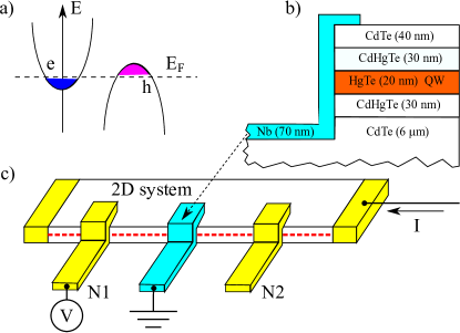
73.40.Qv 71.30.+hRecent interest to transport properties of semimetals is connected with a number of new two-dimensional (2D) systems, like bilayer graphene graphene1 ; graphene2 , BiSe thin films bise and wide HgTe quantum wells kvon ; kvon_s1 ; kvon_s2 . Similarly to a classical bismuth semimetal, all these materials are characterized by a small overlap between the valence and conduction bands, see Fig. 1 (a), so both electrons and holes contribute to transport. In the regime of equal electron and hole concentrations, while recombination between the carriers from different bands is strongly suppressed, Coulomb correlations become important mott ; rice .
Two-component correlated systems are expected to demonstrate non-trivial physics in proximity with a superconductor. In the case of a Weyl semimetal weyl , which is an example of the correlated system, the proximity leads to specular Andreev reflection spec at the interface, or even to superconducting correlations within a semimetal corr1 ; corr2 ; corr3 . Also, a correlated four-particle Andreev process has been predicted bilayer_theor ; golubov at the interface between a superconductor and a bilayer exiton structure bilayer_exp . One can also expect non-trivial proximity effects for ’classical’ 2D semimetals with indirect band structure, because of the allowed exciton formation in the regime of equal electron and hole concentrations rice .
Here, we investigate electron transport through the interface between a niobium superconductor and the edge of a two-dimensional semimetal, realized in a 20 nm wide HgTe quantum well. Experimentally, we observe that typical behavior of a single Andreev contact is complicated by both a pronounced zero-bias resistance anomaly and shallow subgap resistance oscillations with periodicity. These results are demonstrated to be independent of the superconducting material and should be regarded as specific to a 2D semimetal in a proximity with a superconductor. We interpret these effects to originate from the Andreev-like correlated process at the edge of a two-dimensional semimetal.
Our quantum well with (013) surface orientation is grown by molecular beam epitaxy. The layer sequence is shown in Fig. 1 (b), a detailed description can be found elsewhere growth1 ; growth2 . At high nm width, a 2D system in the quantum well represents an indirect 2D semimetal kvon_s1 ; kvon_s2 with a low overlap between the valence and conduction bands, as depicted in Fig. 1 (a). For the undoped well, both electrons and holes contribute to transport. As obtained from standard magnetoresistance measurements, the carriers’ concentrations are low enough, about cm-2 and cm-2 for electrons and holes, respectively. Electrons’ mobility is high enough, about cm2/Vs, because the holes (with lower cm2/Vs mobility) provide efficient disorder screening kvon_scat .
Fig. 1 (c) demonstrates a sample sketch. A 100 m wide mesa is formed by 200 nm deep dry Ar plasma etching. We use magnetron sputtering to deposit a superconducting film over the mesa step, with low (2-3 m) overlap, see Fig. 1 (b-c). The 10 m wide superconducting electrode is formed by lift-off technique, and the surface is mildly cleaned by Ar plasma before sputtering. To avoid mobility degradation, the sample is kept at room temperature during the sputtering process. Ohmic source-drain contacts and the potential probes N1 and N2 are obtained by thermal evaporation of 100 nm thick Au (yellow in Fig. 1 (c)). The potential probes are usually placed at a 100 m distance from the superconducting electrode.
Our samples differ by the material of a superconducting contact. It is formed either by a 70 nm thick film, or by a bilayer from a 35 nm thick layer and a 30 nm thick permalloy layer. In both cases the 2D system is in a direct contact with the Nb film, which ensures similar scattering at the SN (superconductor – semimetal) interface. On the other hand, a premagnetized layer partially suppresses superconductivity in Nb, so the bilayer behaves like a Nb superconductor with a strongly reduced gap.
Without annealing, only a side contact is possible at the mesa step between the metallic electrode (either superconducting or normal) and a 2D system, because of the insulating CdTe layer on the top of the structure, see Fig. 1 (b). We study electron transport across a single SN (Nb – semimetal) junction in a standard three-point technique, see Fig. 1 (c): the superconducting contact is grounded; a current is fed through one of the normal Ohmic contacts; the normal contact N1 (or N2) traces the quantum well potential. We sweep a dc current component from -2 to +2 A. To obtain characteristics, this dc current is additionally modulated by a low ac (30 pA, 110 Hz) component. We measure both, dc () and ac (), components of the quantum well potential by using a dc voltmeter and a lock-in, respectively. The obtained curves are verified to be independent of the mutual positions of the normal Ohmic contacts, so they only reflect the transport parameters, and , of a particular SN (i.e. Nb-2D) interface. We check, that the lock-in signal is independent of the modulation frequency in the 60 Hz – 300 Hz range, which is defined by applied ac filters. To extract features specific to a 2D semimetal, the measurements are performed at a temperature of 30 mK.
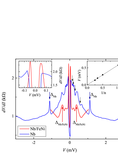
Fig. 2 presents the examples of characteristics of a single SN junction between the edge of a 2D semimetal and the superconducting electrode. The main behavior is consistent with the standard one tinkham of a single Andreev SN junction: every curve demonstrates a clearly defined superconducting gap (denoted by colored arrows), the subgap resistance is undoubtedly finite, which is only possible due to Andreev reflection. The superconducting gap for a single-layer Nb junction 1.15 mV is in a good correspondence with the expected K for niobium. The gap is reduced to meV for a bilayer electrode, as obtained from the red arrows in Fig. 2. The maximum subgap resistance k exceeds the normal junction resistance k, so a single-particle scattering is significant at the Nb-2D interface tinkham . We can be sure, that the upper layer is not affecting the interface scattering, because of the similar for both superconducting materials. A transmission of the interface can be estimated tinkham as , which corresponds to the BTK barrier strength tinkham .
Specifics of the 2D semimetal appears in two striking observations, which can not be expected tinkham for a standard single Andreev contact. (i) The first one is a strong, twice below , zero-bias differential resistance anomaly. The anomaly width and strength are almost the same for a single-layer Nb and for a bilayer , see Fig. 2 and the left inset to it. (ii) The second observation is the shallow subgap resistance oscillations in Fig. 2. They clearly demonstrate periodicity, as depicted in the right inset to Fig. 2. The number of visible oscillations is reduced for , since the available bias range is effectively diminished by the reduced gap at constant zero-bias anomaly width. These features are gradually diminishing with temperature and disappear at 0.62 K–0.88 K for both and junctions, despite the much higher in the last case.
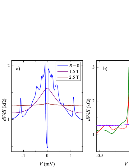
The effect of the magnetic field is more complicated, see Figs. 3, 4. To avoid orbital effects, the field is oriented within the 2D plane (with accuracy) along the mesa edge. Thus, it is strictly in-plane oriented also for the superconducting film at the mesa step. We obtain similar low-field results for the normally oriented magnetic field.
Fig. 3 (a) demonstrates that the superconductivity can be completely suppressed above 2.5 T for the SN junction with a single-layer Nb electrode, which well corresponds to the Nb critical field (about 3 T for our films). In the intermediate fields, e.g. 1.5 T in Fig. 3 (a), the curve is non-linear and monotonous. The zero-bias anomaly and the oscillations are suppressed simultaneously by very low, below 30 mT, magnetic field. Qualitatively similar results are obtained for the junction with a bilayer, see Fig. 3 (b).
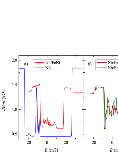
The low-field behavior of the zero-bias resistance anomaly is shown in Fig. 4 (a) in detail. We fix the bias and sweep the magnetic field slowly. For both the superconducting materials, the resistance is almost field-independent within some interval around zero field. At the edges of this interval, both ’s demonstrate step-like increase. This is important, that despite the strongly different for the Nb and electrodes, the zero-bias anomaly is characterized by even quantitatively similar behavior in Fig. 4. We should connect it with a normal side of the junction, i.e. with a 2D semimetal.
One can see some irregular fluctuations in Fig. 4 (a) around zero field. These fluctuations becomes to be extremely strong, if we place the Au potential probe in a close vicinity (5 m) of the superconducting electrode, see Fig. 4 (b). The fluctuations can not be seen outside the zero-bias anomaly (in respect to bias and magnetic field intervals), so they are specific for this regime.
Thus, for transport through a single SN junction between a superconductor and a 2D semimetal, realized in a wide HgTe quantum well, two experimental observations have to be understood: (i) the strong zero-bias resistance dip; (ii) the shallow subgap resistance oscillations with the periodicity. These results are independent of the superconducting material and should be regarded as specific to a 2D semimetal in a proximity with a superconductor gasb .
The curves in Fig. 2 are obtained for a single SN contact. On the other hand, the resonances in the subgap resistance require some space restriction on the normal side of the junction. We can not connect this restriction with trivial disorder: it can only provide a small, weak antilocalization-like, correction at zero bias, known as disorder-enhanced Andreev reflection wal1 ; wal2 . In contrast, the zero-bias resistance drops twice below the normal junction’s value in Figs. 2 and 4. Moreover, trivial backscattering can not provide subsequent energy increase in multiple reflections, which is responsible for the periodicity tinkham . Thus, our experiment essentially demands non-trivial (i.e. Andreev-like) scattering on the normal side of the junction, within the 2D semimetal.
Since the data in Fig. 2 are qualitatively resemble the typical SNS behavior kvon_sns , we have to connect both experimental findings with scattering on some correlated state near the edge of a 2D semimetal. This correlated state can naturally appear in the regime of equal carriers’ concentrations (balance), . The balance regime is necessary realized within the stripe of finite width due to the edge reconstruction shklovskii ; image02 , as depicted in Fig. 5. The edge of the sample is a potential barrier for both electrons and holes konig . In our two-component system, the hole concentration is dominant in the bulk. The edge potential profile is smooth because of electrostatics shklovskii ; image02 , so the carriers’ concentrations are gradually diminishing to the edge. The dominant (hole) concentration is diminishing faster until the regime of equal concentrations is reached. This picture agrees with the observed mesoscopic resistance fluctuations in Fig. 4: the balance stripe is especially sensitive to the long-range potential disorder because of inefficient screening halperin at .
We can propose two possible realizations of a correlated state within the balance stripe.
(i) The simplest way is to assume, following Refs. corr1, ; corr2, ; corr3, , intrinsic superconductive correlations in this regime. In this case a single SN junction effectively behaves as a SNS-like structure, where Josephson current and multiple Andreev reflections (MAR) are naturally allowed tinkham ; kvon_sns .
(ii) Another candidate for the correlated state is the excitonic phase within the balance stripe. In this case one can expect both the coherent transport at low energies bilayer_theor ; golubov (responsible for zero-bias anomaly) and the specific correlated Andreev-like process at the edge of the stripe. The latter is an analogue of the Andreev process proposed in Refs. bilayer_theor, for a bilayer exciton condensate bilayer_exp and of the spinlike Andreev reflection proposed in Refs. wang, ; sham, at the interface of a semimetal and an excitonic phase.
Until now, there are no experimental confirmations for these predictions (i) and (ii), so both these possibilities should be regarded with care. The magnetic field behavior in Fig. 4 is more consistent with the excitonic assumption (ii). Indeed, the induced superconductivity (i) is directly connected with the bulk superconductor. On the other hand, the excitonic phase seems to be independent of the superconductor characteristics. In our experiment, the step-like field dependence in Fig. 4 is almost the same for two strongly different superconducting electrodes and . Thus, the dependence in Fig. 4 should be connected with the magnetic field effect on transport to the excitonic phase.
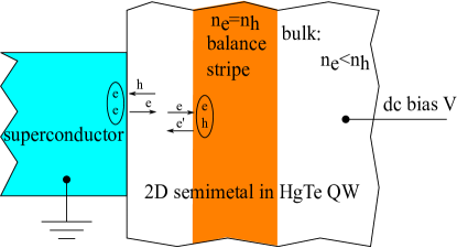
If we consider an electron between the superconductor and the excitonic phase within the balance stripe, see Fig. 5, it experience usual Andreev reflection at the superconductor (left in Fig. 5) interface. At the excitonic (right) interface, charge conservation requires reflection of an electron to add an exciton to the excitonic phase. This electron, however, belongs to a different, ’hole’, band of the semimetal spectrum wang ; sham in Fig. 1 (a), since recombination between the carriers from different bands is strongly suppressed in semimetal. This is the key difference from usual backscattering, which makes this reflection similar bilayer_theor ; golubov ; wang ; sham to usual Andreev process. In a combination with Andreev reflection at the superconductor interface, the subsequent energy increase is allowed in multiple reflections, which seems to be responsible for the oscillations periodicity, observed in our experiment.
As a conclusion, we investigate electron transport through the interface between a niobium superconductor and the edge of a two-dimensional semimetal, realized in a 20 nm wide HgTe quantum well. Experimentally, we observe that typical behavior of a single Andreev contact is complicated by both a pronounced zero-bias resistance anomaly and shallow subgap resistance oscillations with periodicity. These results are independent of the superconducting material and should be regarded as specific to a 2D semimetal in a proximity with a superconductor. We interpret these effects to originate from the Andreev-like correlated process at the edge of a two-dimensional semimetal.
We wish to thank A.M. Bobkov, I.V. Bobkova, Ya. Fominov, V.T. Dolgopolov, and T.M. Klapwijk for fruitful discussions. We gratefully acknowledge financial support by the RFBR (projects No. 13-02-00065 and 13-02-12127), RAS and the Ministry of Education and Science of the Russian Federation under Contract No. 14.B25.31.0007.
References
- (1) B. E. Feldman, J. Martin, and A. Yacoby, Nat. Phys. 5, 889 (2009).
- (2) E. McCann and M. Koshino, Rep. Prog. Phys. 76, 056503 (2013).
- (3) C. Kastl, T. Guan, X. Y. He, K. H. Wu, Y. Q. Li, and A. W. Holleitner, Appl. Phys. Lett. 101, 251110 (2012).
- (4) Z. D. Kvon,E. B. Olshanetsky, D. A. Kozlov, N. N. Mikhailov and S. A. Dvoretskii, JETP Letters, 87, 502 (2008)
- (5) Z. D. Kvon, E. B. Olshanetsky, E. G. Novik, D. A. Kozlov, N. N. Mikhailov, I. O. Parm, and S. A. Dvoretsky, Phys. Rev. B 83, 193304 (2011).
- (6) E. B. Olshanetsky, Z. D. Kvon, Y. A. Gerasimenko, V. Prudkoglyad, V. Pudalov, N. N. Mikhailov, and S. A. Dvoretsky, Pis’ma v ZhETF 98, 947 (2013).
- (7) N. F. Mott, Phil. Mag. 6 , 287 (1961).
- (8) D. Jerome, T. M. Rice, and W. Kohn Phys. Rev. 158, 462 ( 1967)
- (9) A. A. Burkov, M. D. Hook, and L. Balents, Phys. Rev. B 84, 235126 (2011)
- (10) Wei Chen, Liang Jiang, R. Shen, L. Sheng, B. G. Wang, D. Y. Xing EPL 103, 27006 (2013)
- (11) T. Meng and L. Balents, Phys. Rev. B 86, 054504 (2012).
- (12) G. Y. Cho, J. H. Bardarson, Y.-M. Lu, and J. E. Moore, Phys. Rev. B 86, 214514 (2012).
- (13) H. Wei, S. P. Chao, and V. Aji, Phys. Rev. B 89, 014506 (2014).
- (14) Fabrizio Dolcini, Diego Rainis, Fabio Taddei, Marco Polini, Rosario Fazio, and A. H. MacDonald, Phys. Rev. Lett. 104, 027004 (2010); Sebastiano Peotta, Marco Gibertini, Fabrizio Dolcini, Fabio Taddei, Marco Polini, L. B. Ioffe, Rosario Fazio, and A. H. MacDonald, Phys. Rev. B 84, 184528 (2011)
- (15) M. Veldhorst, M. Hoek, M. Snelder, H. Hilgenkamp, A. A. Golubov, and A. Brinkman, Phys. Rev. B 90, 035428
- (16) I. B. Spielman et al., Phys. Rev. Lett. 84, 5808 (2000); I. B. Spielman et al., ibid. 87, 036803 (2001); J. P. Eisenstein and A. H. MacDonald, Nature (London) 432, 691 (2004) and work cited therein.
- (17) N.N. Mikhailov, R.N. Smirnov, S.A. Dvoretsky et. al., Int. J. Nanotechnology, 3, 120 (2006)
- (18) E.B. Olshanetsky, S. Sassine, Z. D. Kvon, et. al., JETP Lett., 84, 661 (2006).
- (19) E. B. Olshanetsky, Z. D. Kvon, M. V. Entin, L. I. Magarill, N. N. Mikhailov, I. O. Parm, and S. A. Dvoretsky, JETP Lett. 89, 290 (2009).
- (20) G.E. Blonder, M. Tinkham, T.M. Klapwijk, Physical Review B, 25, 4515 (1982); M. Tinkham, Introduction to Superconductivity (2d ed., McGraw–Hill, New York, 1996).
- (21) We have reproduced these results for a InAs/GaSb semimetal, so they are also independent of the particular 2D semimetal realization, which will be published elsewhere.
- (22) I. K. Marmorkos, C. W. J. Beenakker, R. A. Jalabert, Physical Review B, 48, 2811 (1993)
- (23) D. I. Pikulin, J. P. Dahlhaus, M. Wimmer, H. Schomerus and C. W. J. Beenakker, New J. Phys. 14, 125011 (2012).
- (24) For an example of experimental observation, see, e.g., Z. D. Kvon, T. I. Baturina, R. A. Donaton, M. R. Baklanov, K. Maex, E. B. Olshanetsky, A. E. Plotnikov, J. C. Portal, Phys. Rev. B 61, 11340 (2000).
- (25) M. König, S. Wiedmann, C. Brüne, A. Roth, H. Buhmann, L. W. Molenkamp, X.-L. Qi, and S.-C. Zhang, Science 318, 766 (2007).
- (26) B.A. Volkov and O.A. Pankratov, Pis’ma Zh. Eksp. Teor. Fiz. 42, 145 (1985) [JETP Lett. 42, 178 (1985)].
- (27) D. B. Chklovskii, B. I. Shklovskii, and L. I. Glazman, Phys. Rev. B 46, 4026 (1992).
- (28) E. Ahlswede, J. Weis, K. v. Klitzing, K. Eberl, Physica E, 12, 165 (2002).
- (29) Michael Knap, Jay D. Sau, Bertrand I. Halperin, and Eugene Demler, Phys. Rev. Lett. 113, 186801 (2014).
- (30) Baigeng Wang, Ju Peng, D. Y. Xing, and Jian Wang, Phys. Rev. Lett. 95, 086608 (2005).
- (31) Massimo Rontani, L. J. Sham, arxiv:1301.1726