The Silicon Vertex Tracker for the
Heavy Photon Search Experiment
Abstract
The Heavy Photon Search (HPS) is a new, dedicated experiment at Thomas Jefferson National Accelerator Facility (JLab) to search for a massive vector boson, the heavy photon (a.k.a. dark photon, ), in the mass range 20-500 MeV/c2 and with a weak coupling to ordinary matter. An can be radiated from an incoming electron as it interacts with a charged nucleus in the target, accessing a large open parameter space where the is relatively long-lived, leading to displaced vertices. HPS searches for these displaced to e+e- decays using actively cooled silicon microstrip sensors with fast readout electronics placed immediately downstream of the target and inside a dipole magnet to instrument a large acceptance with a relatively small detector. With typical particle momenta of 0.5-2 GeV/c, the low material budget of 0.7% per tracking layer is key to limiting the dominant multiple scattering uncertainty and allowing efficient separation of the decay vertex from the prompt QED trident background processes. Achieving the desired low-mass acceptance requires placing the edge of the silicon only 0.5 mm from the electron beam. This results in localized hit rates above 4 MHz/mm2 and radiation levels above 1 MeV neutron equivalent /cm2 dose. Hit timing at the ns level is crucial to reject out-of time hits not associated with the decay products from the almost continuous CEBAF accelerator beam. To avoid excessive beam-gas interactions the tracking detector is placed inside the accelerator beam vacuum envelope and is retractable to allow safe operation in case of beam motion. This contribution will discuss the design, construction and first performance results from the first data-taking period in the spring of 2015.
I Introduction
Recent astrophysical results [1, 2] have generated intense interest in physics models beyond the Standard Model with a new force, mediated by a massive, sub-GeV scale, U(1) gauge boson (a.k.a. the Heavy Photon, Dark Photon or ) that couples very weakly to ordinary matter through ”kinetic mixing” [3, 4]. The existence of such a new force is in accord with astrophysical and cosmological constraints. Its weak coupling to the electric charge could be the only non-gravitational window into the existence of hidden sectors consisting of particles that do not couple to any of the known forces [5].
II The Heavy Photon Search Experiment
The Heavy Photon Search experiment (HPS) is a new fixed-target experiment [6] specifically designed to discover an with m MeV, produced through bremsstrahlung in a tungsten target and decaying into an pair. In particular, the HPS experiment has sensitivity to the challenging region with small cross sections out of reach from collider experiments and where thick absorbers, as used in beam-dump experiments to reject backgrounds, are ineffective due to the relatively short decay length ( m) [7]. This is accomplished by placing a compact silicon tracking and vertex detector (SVT) in a magnetic field, immediately downstream (10 cm) of a thin () target to reconstruct the mass and decay vertex position of the . A rendered overview of HPS is shown in Fig. 1.
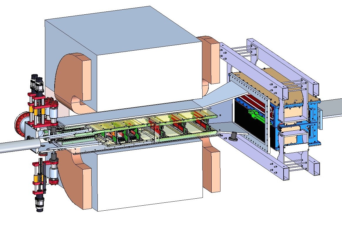
HPS runs in Hall B at Thomas Jefferson National Accelerator Facility (JLab) using the CEBAF accelerator electron beam with an energy of 1.05 GeV and 50 nA current, with planned operation of up to 6.6 GeV and 450 nA. The kinematics of production typically result in final state particles within a few degrees of the beam, especially at low . Because of this, the detector must accommodate passage of the beam downstream of the target and operate as close to the beam as possible. Because background rates in this region from the scattered beam are very large, a fast lead-tungstate crystal calorimeter trigger with 250 MHz flash ADC readout [8] and excellent time tagging of hits is used to trigger on interesting events and reduce the bandwidth required to transfer data from the detector. This method of background reduction is the motivation for operating HPS in a nearly continuous beam: in a beam with large per-bunch charge, background from a single bunch would fully occupy the detector at the required beam intensity.
III The Silicon Vertex Tracking Detector
The Silicon Vertex Tracker (SVT) allows for precise and efficient reconstruction of charged particles and their trajectories. At beam energies between 1.0-6.6 GeV, the electron and positron from the decay will be produced with momenta in the range of 0.4-2 GeV and angles of 10-100 mrad from the beam. The dominant tracking uncertainty in this regime is multiple Coulomb scattering, so the SVT needs to minimize the amount of material in the tracking volume. With an approximate goal of 2% mass resolution in the 1 m long tracking volume (determined by an existing magnet and vacuum chamber) with 0.25 T magnetic field (for 1 GeV beam energy); 1% or less material per 3D tracking hit and six layers was deemed adequate. For weak couplings, the may be long-lived and the pair decay vertex might be displaced several cm downstream of the target foil. To discover rare displaced decays, the SVT typically needs a prompt rejection of roughly 107 at 1 cm vertex resolution [6]. In order to reach that performance, the first layer of the SVT needs to be placed 10 cm from the target. At that distance, the large hit rates from beam electrons undergoing Coulomb scattering in the target allow placing the first layer 1.5 mm from the beam. No instrumentation can be placed inside that 15 mrad angle creating a ”dead zone” throughout the experiment. The expected radiation dose peaks at electrons/cm2/month, or roughly 1 MeV neutron equivalent/cm2/month [9], close to the beam and places further constraints on the sensor technology. Furthermore, the whole tracker has to operate in vacuum to avoid secondary backgrounds from beam gas interactions, and have retractable tracking planes and easy access for sensor replacement to increase safety. Given the high hit density, the fast time response, and good resolution and radiation hardness needed; silicon microstrip sensors are the technology of choice for the tracker. Pixel sensors suitable for instrumenting our large acceptance are either too slow or have an unacceptable material budget.
III-A Layout
| Layer | 1-3 | 4-6 |
|---|---|---|
| pos. (cm) | 10-30 | 50-90 |
| Stereo angle (mrad) | 100 | 50 |
| Non-bend plane resolution (m) | ||
| Bend plane resolution (m) |
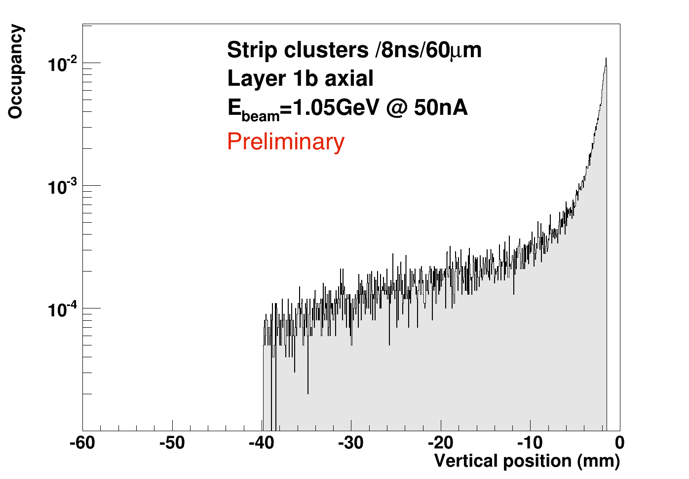
Each of the six tracking layers, arranged in two halves both above and below the beam to avoid the ”dead zone”, consists of silicon microstrip sensors placed back-to-back. The first three layers have a 100 mrad stereo angle between the sensors and the last three have 50mrad in order to improve the pointing resolution to the vertex. The first layer is located only 10 cm downstream of the target to give excellent 3D vertexing performance which, with the 15 mrad dead zone above and below the beam axis, puts the active silicon only 1.5 mm from the center of the beam. Hit densities in the most active region reach 4 MHz/mm2 and about 1% occupancy for the strips closest to the beam, see Fig. 3.
III-B Sensors and Front-End Readout
The sensors are -on-, single-sided, AC-coupled, polysilicon-biased microstrip sensors fabricated by Hamamatsu Photonics Corporation for the cancelled DØ Run 2b upgrade [10]. These m thick sensors are cm2 with 30 and 60 m pitch for sense and readout strips, respectively, matching the required material budget and single hit spatial resolution. The sensors were qualified to withstand at least 1 kV bias in order to tolerate the 1 MeV neutron equivalent/cm2 for a six month run without significant degradation.
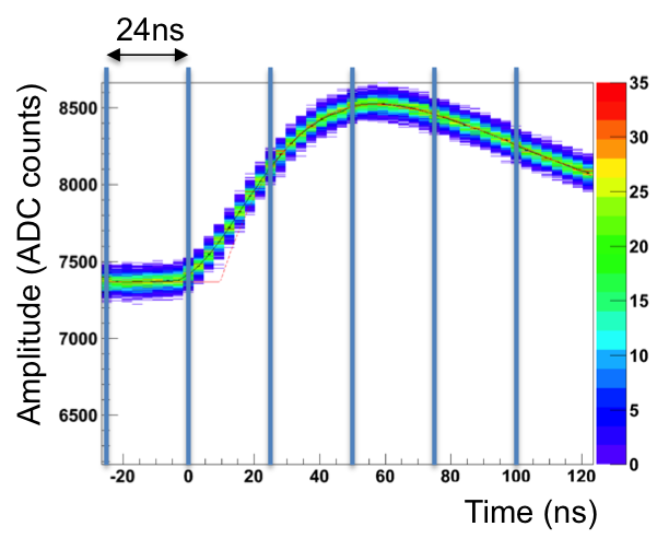
One of the key requirements for the SVT is hit time resolution of ns in order to reject background and improve pattern recognition accuracy for close to the beam where occupancies are high. This is achieved by using the APV25 front-end readout ASIC [11], developed for the Compact Muon Solenoid experiment at the Large Hadron Collider. The APV25 is an analog pipeline ASIC with 128 channels of preamplifier and shaper, feeding a 192 long analog memory pipeline. In the so-called ”multi-peak” readout mode, the APV25 presents three consecutive samples of the pulse height in response to an APV25 readout trigger signal. By sending two APV25 readout triggers for every event trigger signal from the electromagnetic calorimeter, six analog samples of the pulse shape, see Fig. 4, are obtained at a sampling rate of 41 MSPS. This pulse shape can be analyzed and fitted to extract the t0 of the hit [12].
The main parameters of the APV25 ASIC are shown in Tab. II: the 44 m pitch, low noise and operation using either polarity together with the proven robustness and radiation hardness is a good fit for HPS.
| Technology | 0.25 m |
|---|---|
| Channels | 128 |
| Input pitch | 44 m |
| Noise [ENC e-] | C (pF) |
| Power consumption | 350mW |
The sensor and APV25 chip can be seen in Figure 5.
III-C Module Design
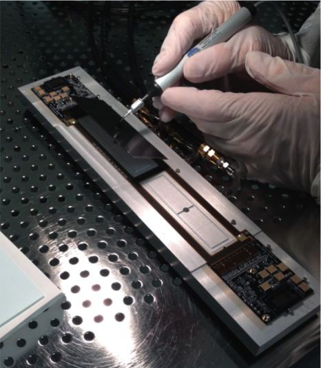
Five APV25 chips are mounted on a FR4 hybrid board and wire-bonded to the end of the sensor. The hybrid boards, located outside the tracking volume, provide power and filtering circuitry for the high voltage bias and a temperature sensor. A hybrid and a sensor, glued to a polyimide-laminated carbon fiber composite backing, make up a so-called ”half-module” for the first three layers and were re-used from the HPS Test detector [13]. To increase acceptance, the half-modules for layers 4-6 have two sensors mounted end-to-end and are read out from opposite ends. Space constraints required these hybrids to be slightly smaller and instead of Teflon-coated twisted pair wires soldered directly to the FR4 board as in layer 1-3, these have high density connectors to transfer signal, power and high voltage bias on and off the hybrid. Figures 5 and 6 show a complete layer 1-3 and a 4-6 half-module under assembly, respectively.
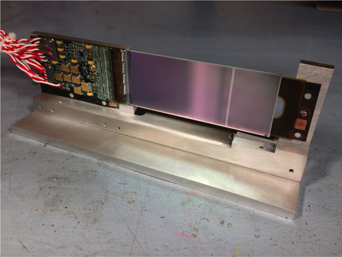
Modules are built by placing two half-modules back-to-back sandwiched around a aluminum cooling block at the hybrid end. The required 3D space point resolution is obtained by rotating one half-module by 50 or 100 mrad. For layer 1-3 modules, the cooling block serves as the fixed part of a support where the opposite end of the half-modules are screwed to an aluminum bar with a pivot engaging a screw-adjusted spring, as shown in Fig. 5. This spring-tensioned module support allows holding the sensors, with their carbon fiber backing, straight with very little support material and absorbs thermal expansion mismatch. The same principle is used for layer 4-6 where the cooling block at one end has an integrated spring pivot.
III-D Support and Cooling
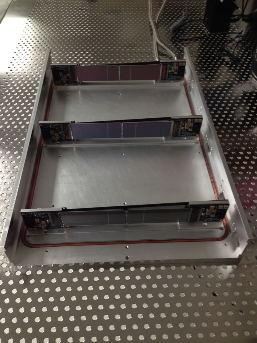
Three modules are screwed directly on an aluminum ”u-channel”, see Fig. 7 and 8, that are actively cooled by HFE 7000 coolant circulating in a 1/4” copper tube pressed into a machined groove.
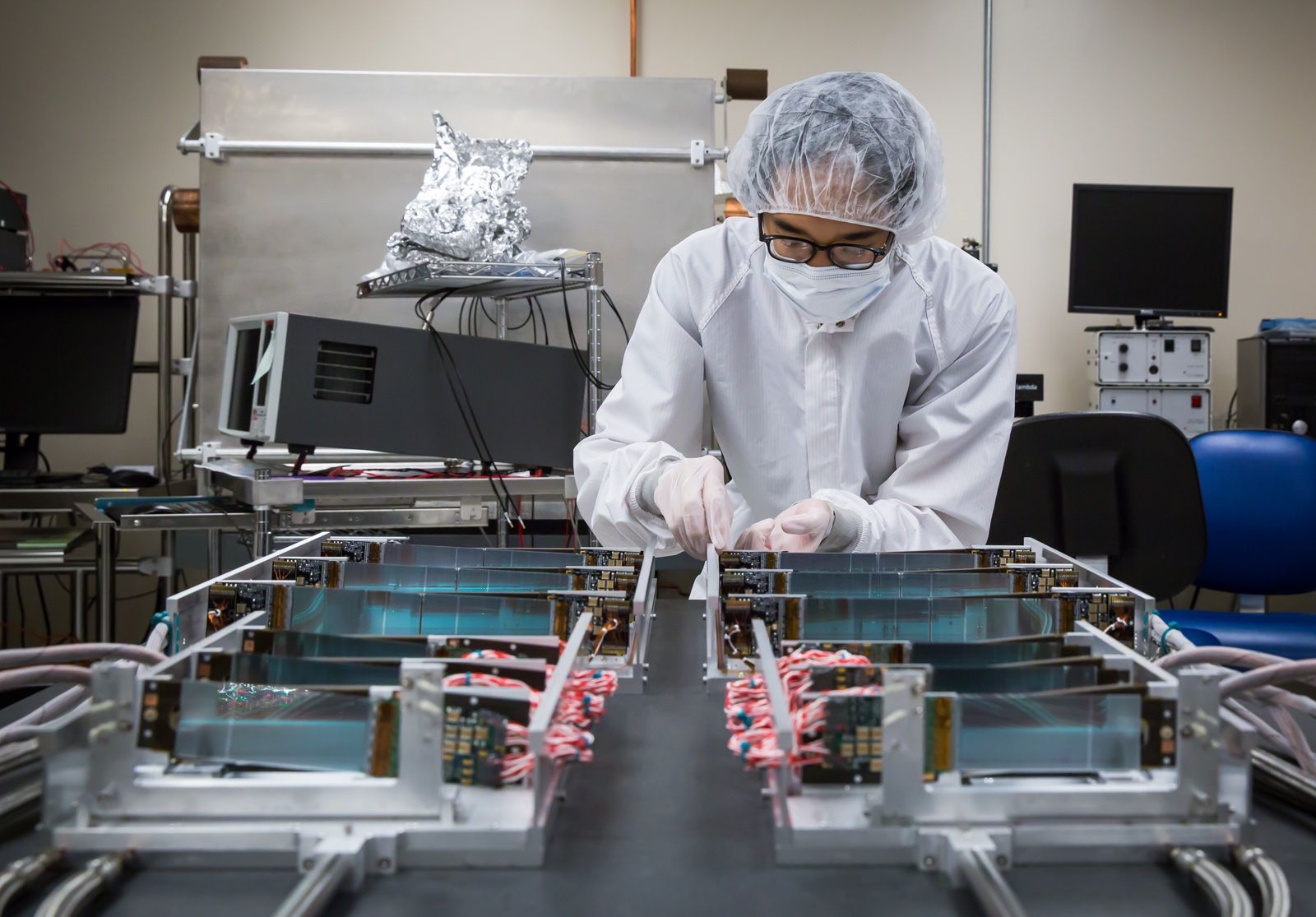
Four U-channels, two for layer 4-6 and two for layer 1-3, roll into a rigid support box on guide rails to precision kinematic mounts. The support box, shown in Fig. 9, sits inside the JLab Hall B analyzing magnet vacuum chamber on four adjustable supports. In order to provide the rigidity needed for precision mounting of the u-channels, a rectangular ”support ring” is located at the inner mounting point for the u-channels.
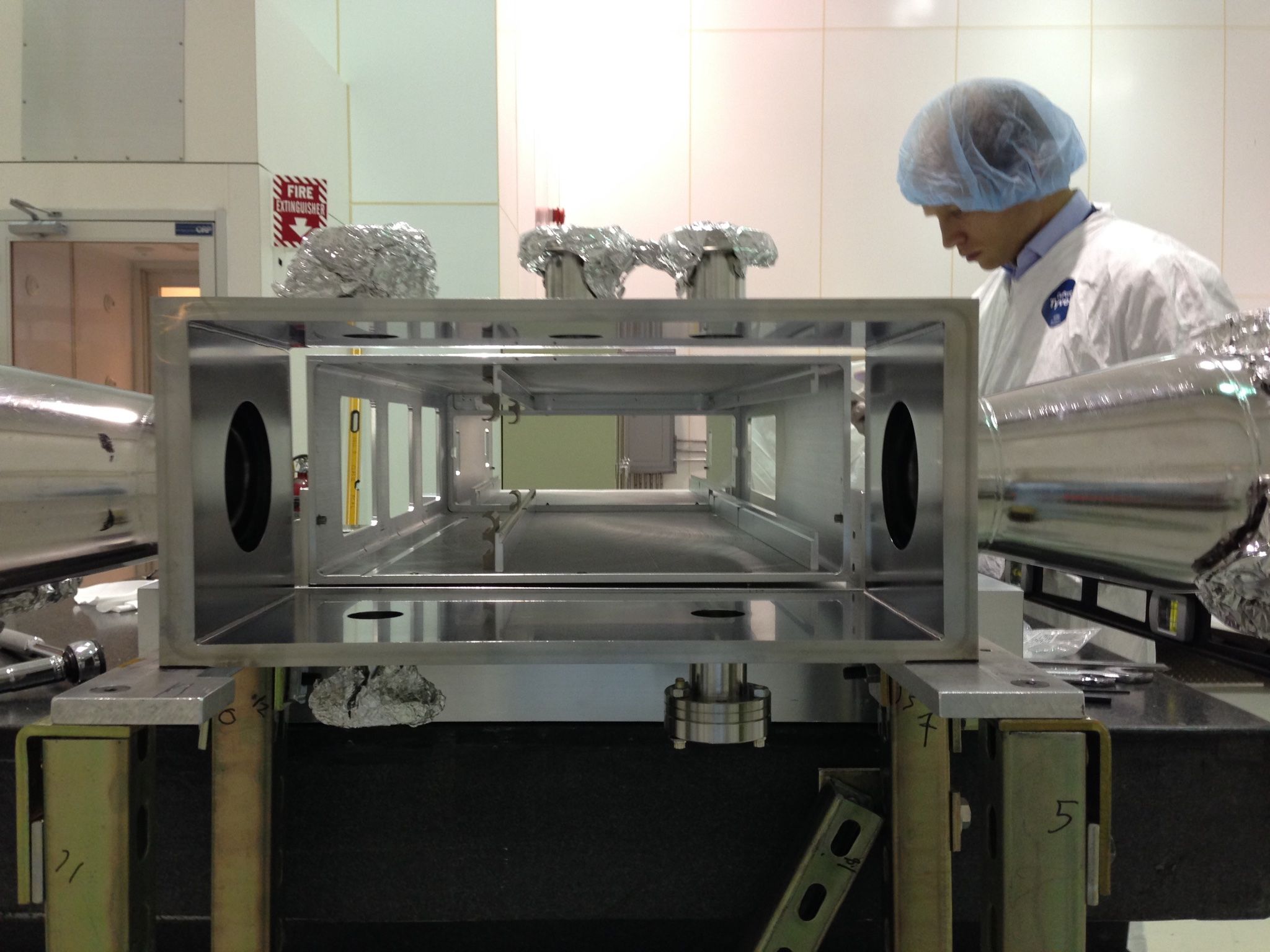
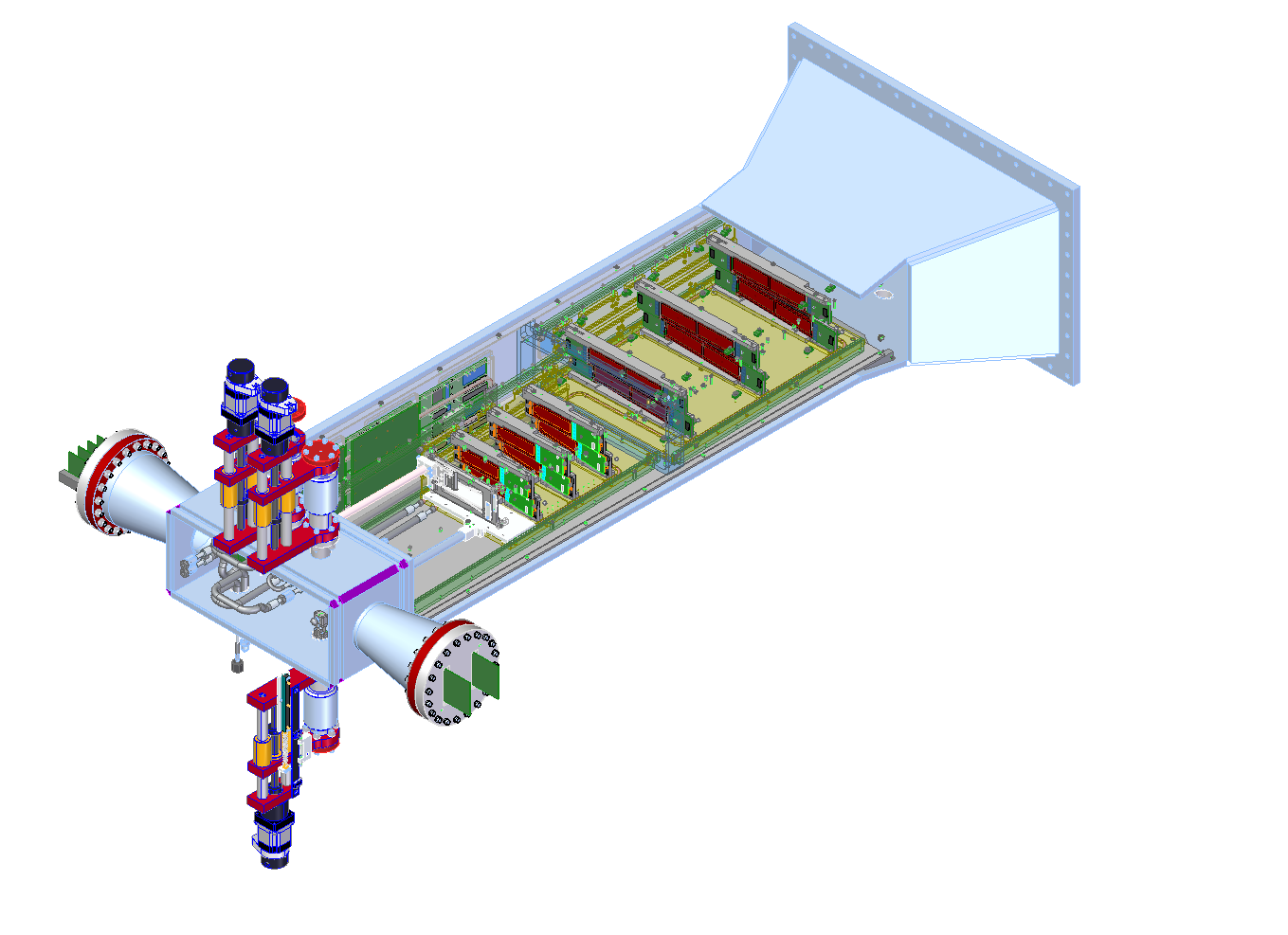
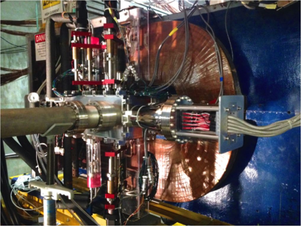
The upstream end of the layer 1-3 u-channels is attached to a rigid support rod extending upstream to vertical linear shifts. Moving the vertical linear shifts allows the layer 1-3 u-channels to rotate up to 1.3∘ and the layer 1 sensors to move more than 7 mm from the beam, allowing clean passage of the beam during beam setup. The linear shifts, one for top and one for bottom, penetrate vacuum through bellows and are remote-controlled by a precision stepper motor. The sensors closest to the beam can be positioned with 6 m steps and m reproducibility. A similar linear shift setup is used to hold and move the target in and out of the beam. The flanges for vacuum penetration are located on a custom support box that attaches to the upstream end of the magnet as seen in Fig. 10. In addition to the linear shift flanges, it has flanges for cooling lines and electrical services and the upstream interface to the beamline.
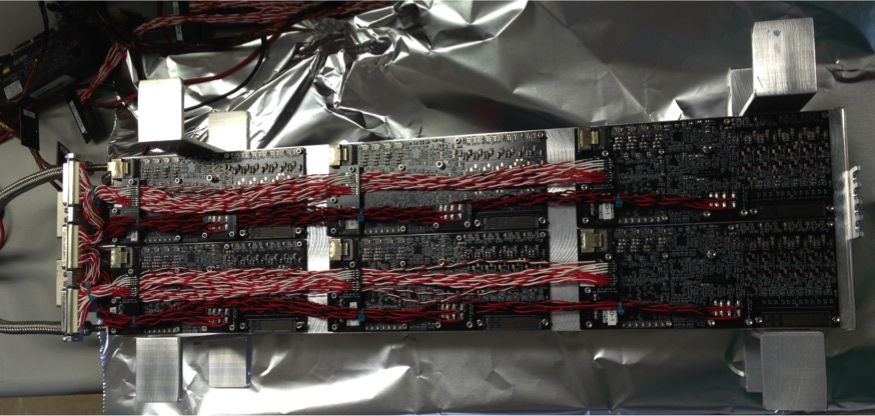
An aluminum plate with data acquisition boards, see Fig. 11, slides into the chamber in a machined groove in the support box.
Coolant is circulated through the u-channels (at about -20∘ C) keeping the silicon at approximately -10∘ C to improve performance after radiation damage. Water at 20∘ C is used to cool the data acquisition boards.
III-E Data Acquisition
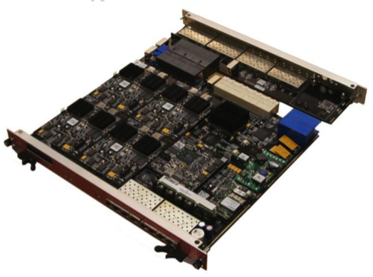
Analog samples at 41.667 MSPS from the APV25 chips are sent on twisted pair magnet wire to a total of 10 Front End Boards (FEB) seen in Fig. 11. Each FEB digitizes and transfers data, from up to four hybrids, at up to 3.3 Gb/s using high-speed serial links to Xilinx Zynq based data processing modules on the ATCA based SLAC RCE platform [13] for zero suppression and event building. Each FEB also handles power regulation and monitoring as well as high voltage sensor bias distribution to each of the attached hybrids. To shorten the analog signal distance, the FEBs are placed inside the vacuum chamber, pressed against thermal pads on each side of a 1/2 cooled support plate on the upstream positron side, rendering a less intense radiation environment. Borated high-density polyethylene is used to further lower the risk of damage from radiation emitted by the nearby target.
Data from the FEBs are routed via short, flexible miniSAS cables to four flange boards. These are FR4 boards potted through slots in the 8” vacuum flange on the upstream positron side of the vacuum box. On the out side of the boards, signals are converted to optical and transferred to the DAQ platform about 30 m away. A similar mechanical technique is used on the opposite side of the vacuum box to bring in low voltage power and high voltage sensor bias into the chamber; this can be seen in Fig. 10.
An overview of the data flow across the RCE platform is shown in Fig. 13.
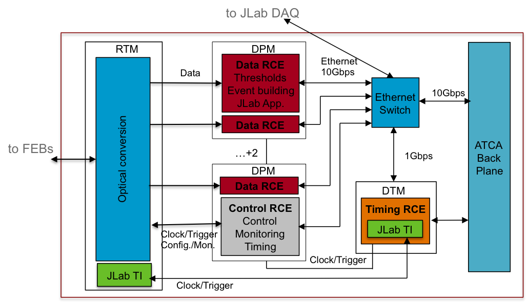
Data from 10 FEBs are split and sent to 14 processing nodes on two ATCA blades, called COBs (Cluster on board). The processing nodes, known as Reconfigurable Cluster Elements (RCE) are based on Xilinx Zync 7000 series system-on-chip which has a dual ARM Cortex A9 processor tightly coupled to a 28nm FPGA fabric. The independent operating nodes receive data from up to four hybrids, apply calibrated thresholds and build event frames in the firmware. A readout application from the JLab DAQ [14], running on the ARM processor, pulls the event frames from memory via DMA and transfers the event frames to the JLab DAQ event builder over 10 Gb/s ethernet. The COB also hosts a special RCE that handles the trigger and timing distribution across the processing nodes on each COB. This RCE implements the JLab trigger interface firmware and accepts the master clocks together with trigger information from the JLab DAQ from a special fiber attached on the custom rear transition board. One of the RCEs is allocated to handle control, trigger and timing signals to and from all the hybrids. It also hosts the slow control and environmental interfaces to the EPICS control system.
During running the system operated at about 20 kHz and with data rates up to 150 MB/s. It has been tested to 50 kHz and 200 MB/s.
III-F Performance
The first run of HPS with an electron beam was carried out in the spring of 2015. A primary goal of this engineering run was to prove the operational principles. Thanks to a 2-week extension of the running schedule HPS was able to take data with beam current and beam size as desired and the SVT in its nominal position with sensor edges only 0.5 mm from the the center of the beam. In all, roughly 1/3 of a week of physics data was taken at the nominal operating point with 1.05 GeV beam energy.
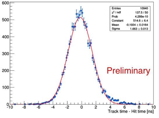
The SVT was operated with 180 V sensor high-voltage bias and had only five bad channels out of 23,004. Beam halo and occupancies were measured as expected (see Fig. 3). The preliminary results presented below show that key performance observables behave as expected at this early stage, where improvements in calibration and alignment are expected. A 2.2 ns time resolution can be extracted from the difference between the hit and track time (average of the hit times on the track) seen in Fig. 14.
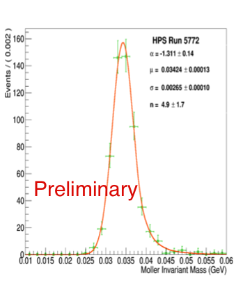
Further optimizations on the pulse shape fit will likely improve this. For the searches, the mass and vertex resolutions are key observables. The mass resolution is calibrated using e.g. Möller events, see Fig. 15; the data show good agreement with the expected distribution from simulated events.
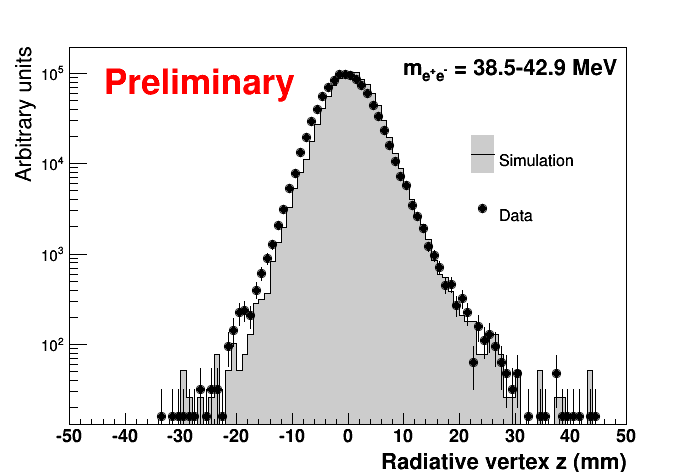
The vertex distribution of e+e- pairs after radiative QED trident selections in Fig. 16 show reasonable agreement with simulation at this stage. Understanding the tails of these distributions is fundamental to the displaced vertex search.
Results from this run are expected in 2016.
III-G Summary and Outlook
The SVT for the HPS experiment was designed and built during 2014. It has six layers of silicon microstrip sensor pairs with 50-100 mrad stereo angle distributed over approximately 80 cm and sits inside a dipole magnetic field. It is placed only 10 cm behind a thin tungsten target and with sensor edges only 0.5 mm from the beam to achieve the prompt e+e- vertex rejection and the acceptance close to the beam.
The SVT was successfully commissioned together with the whole HPS experiment at nominal operating conditions during a run in the spring of 2015. Preliminary results show expected occupancies and backgrounds with reasonable agreement between data and simulated events for key performance observables such as the mass and vertex resolution. Results are expected in the spring of 2016.
The SVT has been kept cold since the run to mitigate reverse annealing in the irradiated sensors in preparation for continuing running in 2016.
Acknowledgment
The authors are grateful for the support from Hall B at JLab and especially the Hall B engineering group for support during installation and decommissioning. They also would like to commend the CEBAF personnel for good beam performance during the spring run of 2015. The tremendous support from home institutions and supporting staff also needs praise from the authors.
References
- [1] O. Adriani et al. [PAMELA Collaboration], Nature 458, 607 (2009)
- [2] M. Ackermann et al. [Fermi LAT Collaboration], Phys. Rev. D 82, 092004 (2010)
- [3] N. Arkani-Hamed, D. P. Finkbeiner, T. R. Slatyer and N. Weiner, Phys. Rev. D 79, 015014 (2009).
- [4] B. Holdom, Phys. Lett. B 166, 196 (1986), P. Galison et al, Phys. Lett. B 136 (1984) 279
- [5] J. L. Hewett, et al., “Fundamental Physics at the Intensity Frontier,” arXiv:1205.2671 [hep-ex].
- [6] A. Grillo et al. [HPS Collaboration], JLab PAC37 PR-11-006, http://www.jlab.org/exp prog/PACpage/PAC37/proposals/Proposals/
- [7] J. D. Bjorken, R. Essig, P. Schuster and N. Toro, Phys. Rev. D 80, 075018 (2009) [arXiv:0906.0580 [hep-ph]].
- [8] E.Jastrzembski and H. Dong, https://coda.jlab.org/drupal/content/vme-payload-modules
- [9] Rashevskaya et al., Radiation damage of silicon structures with electrons of 900-MeV, Nucl. Instr. Meth. A, 485, 126-132, (2002)
- [10] D. S. Denisov and S. Soldner-Rembold, FERMILAB-PROPOSAL-0925.
- [11] M.J. French et al., Design and results from the APV25, a deep sub-micron CMOS front-end chip for the CMS tracker , Nucl. Instr. Meth. A, 466, 359-365 (2001)
- [12] Friedl et al. (2009), Readout of silicon strip detectors with position and timing information, Nucl. Instr. Meth. A, 598, 82-83 (2009)
- [13] P. Hansson Adrian et al. [HPS Collaboration], The Heavy Photon Search test detector, Nucl. Instr. Meth. A 777 (2015), 91-101, http://dx.doi.org/10.1016/j.nima.2014.12.017
- [14] https://coda.jlab.org