Nano-scale strain engineering of graphene and graphene-based devices
Abstract
Structural distortions in nano-materials can induce dramatic changes in their electronic properties. This situation is well manifested in graphene, a two-dimensional honeycomb structure of carbon atoms with only one atomic layer thickness. In particular, strained graphene can result in both charging effects and pseudo-magnetic fields, so that controlled strain on a perfect graphene lattice can be tailored to yield desirable electronic properties. Here we describe the theoretical foundation for strain-engineering of the electronic properties of graphene, and then provide experimental evidences for strain-induced pseudo-magnetic fields and charging effects in monolayer graphene. We further demonstrate the feasibility of nanoscale strain engineering for graphene-based devices by means of theoretical simulations and nano-fabrication technology.
I Introduction
The advances of nano-science and technology have enabled new approaches to designing and controlling the properties of materials at the atomic and molecular length scales. Graphene, a single layer of carbon atoms forming a honeycomb lattice structure, exhibits many interesting properties 1 ; 2 ; 3 and have shown significant dependence of the electronic properties on the nanoscale structural distortion, largely because of the nano-material nature and the characteristics of the Dirac fermions, 4 ; 5 ; 6 ; 7 ; 8 ; 9 ; 10 ; 11 ; 12 which are massless, relativistic carriers of graphene with a linear energy-momentum dispersion relation. 1
In general, structural distortions in graphene may be associated with surface ripples, topological defects, adatoms, vacancies, and extended defects such as edges, cracks and grain boundaries. 1 ; 4 ; 5 ; 6 ; 7 ; 8 The distortion-induced strain 9 in the graphene lattice typically gives rise to two primary effects on the Dirac fermions. One is an effective scattering scalar potential 4 ; 5 ; 6 and the other is an effective gauge potential. 7 ; 8 For instance, compression and dilation distortion can lead to charging effects in localized regions, 1 ; 4 ; 5 ; 6 which has been manifested as strain-enhanced local density of states by scanning tunneling microscopic and spectroscopic (STM/STS) studies of graphene 10 that was grown by means of the high-temperature chemical vapor deposition (CVD) technique. 13 ; 14 It has also been theoretically proposed that certain controlled strain can induce a nearly uniform pseudo-magnetic field by lifting the valley degeneracy of graphene. 12 ; 13 This prediction was first verified empirically via STM/STS studies of graphene nano-bubbles grown on Pt(111) substrates, 11 and subsequently reported in thermal CVD-grown graphene on copper. 10 The presence of significant pseudo-magnetic fields could lead to the localization of Dirac fermions, whereas the charging effect could lead to strong scattering of Dirac fermions, both contributing to the reduction of electrical mobility. Further, extended structural distortion may lead to long-range symmetry breaking, giving rise to fundamental changes in the electronic bandstructures such as gap opening in the Dirac spectra and spontaneous local time-reversal breaking. 12 ; 15 ; 16 The symmetry-breaking distortion may give rise to novel gauge potentials, such as certain non-Abelian gauge potentials 15 and the Kekule distortion, 16 yielding novel electronic states such as fractionally quantized energy spectra as seen in STS studies of strained graphene. 10 ; 12
The susceptibility of graphene to structural distortions can in fact provide opportunities for engineering unique electronic properties of graphene. 17 For instance, the presence of pseudo-magnetic fields could be applied to the development of “valleytronics” 18 ; 19 ; 20 by lifting the valley degeneracy of graphene. Proper nanoscale strain engineering may also produce tunable electronic density of states for nano-electronic devices such as electron beam collimators/deflectors or field effect transistors. 17 ; 20 On the other hand, the feasibility of nanoscale strain engineering relies on the premise of subjecting an ideal graphene sheet to controlled structural distortion. While exfoliated graphene could achieve nearly ideal graphene characteristics, the extremely small sheets and the non-scalable approaches to the production are not compatible with strain-engineering of practical devices. Alternatively, chemical vapor deposition (CVD) techniques at high temperatures (C) have been shown to produce large sheets of graphene, 13 although the resulting graphene often reveals significant spatial strain variations 10 unless numerous additional processing steps were taken. 14 The presence of uncontrollable strain distribution would not be suitable for nanoscale strain-engineering. In this context, the capability of reproducibly growing sizable high-quality and strain-free graphene is necessary for realizing the concept of strain engineering.
We have recently developed a new growth method based on plasma-enhanced chemical vapor deposition (PECVD) at reduced temperatures. 21 This new method has been shown to reproducibly achieve, in one step, high-mobility large-sheet graphene samples that are nearly strain free, 21 paving the way for realization of nanoscale strain-engineering. The objective of this work is to demonstrate the feasibility of nanoscale strain-engineering of graphene by means of both theoretical simulations and empirical development of PECVD-grown graphene on nanostructured substrates. The correlation between realistic designs of nanoscale strain distributions and the resulting effects on the electronic properties of graphene is evaluated by means of molecular dynamics. Empirical proof of concept for nanoscale strain engineering via nanostructured substrates for graphene is also demonstrated and compared with theoretical simulations. Finally, we discuss feasible device applications based on nanoscale strain-engineering of graphene.
II Effects of structural distortions on the electronic properties of graphene
The physical causes for the strain-induced effective scalar and gauge potentials in graphene may be understood in terms of the changes in the distance or angles between the orbitals that modify the hopping energies between different lattice sites, thereby giving rise to the appearance of a vector (gauge) potential and a scalar potential in the Dirac Hamiltonian. 1 ; 7 Under the preservation of global time-reversal symmetry, the presence of strain-induced vector potential leads to opposite pseudo-magnetic fields and for the two inequivalent Dirac cones at and , respectively. On the other hand, the presence of a spatially varying scalar potential can result in local charging effects known as self-doping. 1
II.1 Overview of the effect of strain on Dirac fermions of graphene
As mentioned in the introduction, disorder generally induces two types of contributions to the original Dirac Hamiltonian . One is associated with the charging effect of a scalar potential, and the other is associated with a pseudo-magnetic field from a strain-induced gauge potential. For an ideal graphene sample near its charge-neutral point, the massless Dirac Hamiltonian in the tight-binding approximation is given by: 1
| (1) |
where () annihilates (creates) an electron with spin () on site of the sublattice A, () annihilates (creates) an electron with spin on site of the sublattice B, eV ( eV) is the nearest-neighbor (next-nearest-neighbor) hopping energy for fermion hopping between different sublattices, and refers to the Hermitian conjugate. 1
The presence of lattice distortion results in a spatially varying in-plane displacement field and a spatially varying height displacement field . Therefore, in addition to changes in the distances or angles among the two-dimensional -bonds, distortion also induces changes in the distance or angle between the orbitals. Such three-dimensional lattice distortion gives rise to the following expressions for the strain tensor components (where = ): 1
| (2) |
so that an additional perturbative Hamiltonian must be introduced to describe the wave-functions of Dirac fermions in distorted graphene: 1 ; 4 ; 5
| (3) | |||||
where and are strain-induced modifications to the nearest and next nearest neighbor hopping energies, respectively, represents the () Pauli matrices, denotes the spinor operator for the two sublattices in the continuum limit, and () represents the strain-induced perturbation to the scalar (gauge) potential. We note that in the event of finite -axis corrugation, the modified hopping integrals for Dirac fermions from one site to another must involve not only the in-plane orbitals but also the orbitals of the distorted graphene sheet as the result of the three-dimensional distribution of electronic wavefunctions.
Specifically, the strain-induced gauge potential in Eq. (3) is related to the two-dimensional strain field by the following relation (with the x-axis chosen along the zigzag direction): 4 ; 5
| (4) |
where nm is the nearest carbon-carbon distance, and is a constant ranging from 2 to 3 in units of the flux quantum 1 . Similarly, the compression/dilation components of the strain can result in an effective scalar potential in addition to the aforementioned pseudo-magnetic field so that there may be a static charging effect 4 ; 5 ; 6 . Here is given by: 4 ; 5 ; 6
| (5) |
where eV, and is the dilation/compression strain.
By inserting the explicit expressions given in Eqs. (2), (4) and (5) into Eq. (3), we find that the excess strain components associated with the changes in the distances and angles of the -orbitals may be written in forms of and , respectively. We further note that in the event of strong -axis corrugation, the strain components resulting from the variations in the -orbitals may become dominant over the in-plane strain components according to Eq. (2).
Thus, the total Hamiltonian for the Dirac fermions of graphene becomes . The physical significance of the perturbed term is analogous to the contribution of a vector potential in a two-dimensional electron gas that gives rise to a vertical magnetic field and the formation of quantized orbitals. In this context, the Landau levels of Dirac fermions under a given satisfy the following relation: 1
| (6) |
where denotes the Fermi velocity of graphene and denotes integers. Additionally, the magnetic length associated with a given is ( in units of Tesla). 1 Similarly, the physical significance of the perturbed term is analogous to the contribution from a scalar potential . For strain primarily induced by corrugations along the out-of-plane () direction, the typical strain is of order from Eq. (2), where denotes the height fluctuations and is the size of the lateral strained region. In principle the charging effect associated with the scalar potential can be suppressed in a graphene layer suspended over a metal if . 7 ; 8 However, for , the strain-induced charging effect can no longer be effectively screened so that experimental observation of such an effect at the nanoscale may be expected. 10 ; 12
II.2 Empirical manifestation of giant pseudo-magnetic fields and local charging effects in strained graphene by STM/STS
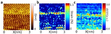
Significant charging effects and giant pseudo-magnetic fields in nanoscale strained graphene have been manifested by STM/STS studies of thermal CVD-grown graphene. 10 ; 11 ; 12 As exemplified in Fig. 1a for atomically resolved topography of a CVD-grown graphene on copper, significant lattice distortion along a ridge line is clearly visible. Using Eq. (5), the corresponding compression/dilation strain map obtained from the lattice distortions in Fig. 1a is shown in Fig. 1b, and the empirically determined zero-bias conductance map of the same area is shown in Fig. 1c. We find strong correlation among the maps of topography, strain and the tunneling conductance.
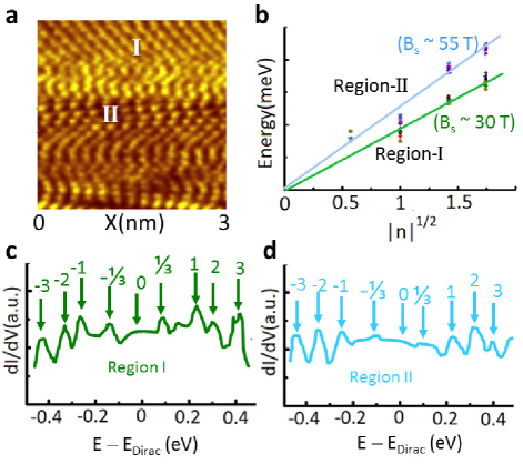
Empirically, the pseudo-magnetic fields can be determined from the strain-induced quantized conductance peaks superposed onto of the Dirac spectrum 7 ; 8 ; 10 ; 11 according to Eq. (6). As exemplified in Fig. 2, the tunneling conductance of strained graphene revealed quantized spectral peaks in addition to the generic Dirac tunneling spectrum. By plotting the peak positions in energy relative to the Dirac point versus , where being integers or fractional numbers () with and being an integer, 10 ; 12 we could identify the magnitude of by using Eq. (6). From Fig. 2, we note that the pseudo-magnetic fields exhibited spatial variations depending on the local strain, and larger strain generally induced stronger values. The strain-induced giant pseudo-magnetic fields, on the order of tens of Tesla, have the effect of confining the motion of Dirac fermions to the magnetic length , similar to the formation of electronic cyclotron orbit under an external magnetic field. Hence, the mobility of Dirac fermions becomes substantially compromised under the presence of giant pseudo-magnetic fields.
II.3 Empirical manifestation of macroscopic strain effects by Raman spectroscopy
The structural distortion-induced strain effects on graphene can also be determined by examining the Raman spectroscopy. 22 ; 23 Specifically, the biaxial strain in the PECVD-graphene on Cu can be estimated by considering the Raman frequency shifts and the Gruneisen parameter : 22 ; 23
| (7) |
where (= , 2) refers to the specific Raman mode. 22 ; 23 Using and , we can determine the average strain of graphene samples prepared under different conditions. As exemplified in Fig. 3a-d for the comparison of the Raman spectroscopy taken on a thermal CVD-grown graphene and a low-temperature PECVD-grown graphene, we found a general trend of downshifted G-band and 2D-band frequencies for all PECVD-grown graphene relative to thermal CVD-grown graphene on the same substrate, 21 indicating reduced strain in PECVD-grown graphene.
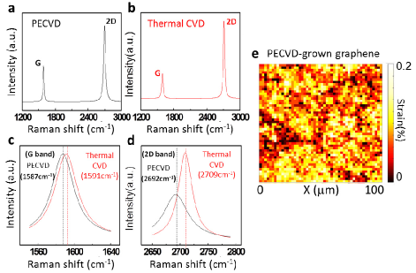
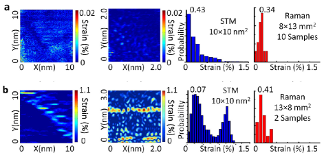
In general, using Eq. (7) we can determine the spatial strain distribution in a graphene sample over a substantially large area, as illustrated in Fig. 3e for a low-temperature PECVD-grown graphene sample over an area of that appears to be nearly strain-free with an average of 0.07% strain. This is in sharp contrast to the significant strain-induced effects found in thermal CVD-grown graphene. As further illustrated in Fig. 4 for both atomically resolved topographic studies by means of STM and for macroscopic-scale studies over multiple areas per sample and for multiple samples by means of Raman spectroscopy, we found that for the same Cu-foil substrates, the average strain in PECVD-grown graphene was consistently more than one order of magnitude smaller than that of our typical thermal CVD-grown graphene.
While the magnitude of strain derived from Raman spectroscopy with Eq. (7) does not contain the shear strain components, we remark that the information thus derived is still largely proportional to the total strain obtained from the displacement fields (, measured by STM) accordingly to Eq. (2) if the symmetry between and components is preserved and the -axis corrugation dominates. This is the reason why the empirical strain distributions shown in Fig. 4, which were obtained from both STM and Raman spectroscopic studies, are mostly consistent.
Our finding of much reduced strain is also consistent with the much better electrical mobility in the PECVD-grown graphene, typically at 300 K, which is more than one order of magnitude better than that of thermal CVD-grown graphene. 21 The availability of nearly strain-free graphene by means of our PECVD growth method clearly paves the way to strain-engineering of the electronic properties of graphene.
Having demonstrated the effect of strain on the electronic properties of graphene and our ability of developing nearly strain-free graphene, our next step is to employ theoretical simulations to assist our empirical designs of nanostructures on substrates in order to induce the desirable strain for graphene overlay on these substrates.
III Theoretical simulations of strain-induced psuedo-magnetic fields
We employed molecular dynamics (MD) techniques to compute the spatial distributions of the displacement field, strain tensor and pseudo-magnetic field for given engineered nanoscale structural distortions to graphene. For simplicity, we chose either a nano-sphere or a nano-hemisphere with a varying radius as the building block for constructing different nanostructures on the substrate.
III.1 Methods of the simulations
For the MD simulations, we used the software package LAMMPS, which is available on the website http://lammps.sandia.gov. We considered a monolayer squared-shape graphene sheet with a fixed number of monolayer carbon atoms, and assumed that the positions of the carbon atoms at the boundaries of this graphene sheet remained invariant throughout the simulations. To induce structural distortions, we moved the graphene sheet adiabatically towards either a nano-sphere or a nano-hemisphere of gold nanoparticle until a desirable maximum height relative to the boundaries of the graphene sheet was reached (Fig. 5a-b), and then relaxed the entire system until it reached equilibrium. Here the load necessary to move the graphene sheet towards the nanostructure was comparable to the combined effect of ambient air pressure and gravity.
Next, to ensure that the intrinsic properties of graphene were largely preserved without significant perturbations from the nanostructured substrate, we assumed that the attractive coupling between the graphene sheet and the underlying nanostructured substrate was sufficiently weak that it did not directly affect the graphene Hamiltonian. On the other hand, the attractive interaction must also be sufficiently strong to ensure proper conformation of graphene to the nanostructured substrate. We found that this situation could be realized by inserting a monolayer of hexagonal boron nitride (h-BN) in-between the graphene sheet and the nanostructure/substrate, provided that the crystalline structure of the h-BN layer was aligned at an incommensurate angle relative to the graphene sheet so that no superlattice structures formed within the finite sheet of graphene under consideration.
The rationale for the choice of h-BN for the substrate material was based on the empirical fact that graphene on h-BN exhibited as excellent electrical mobility and fractional quantum Hall effects as those of suspended pristine graphene, in sharp contrast to substantially degraded mobility of graphene on other substrates (such as SiO2/Si). Therefore, we employed realistic parameters for the van der Waals interaction of BN with carbon atoms and assumed isothermal conditions throughout the simulations described in Section 3. We also applied h-BN to all nanostructured substrates for empirical strain-engineering of graphene to be discussed in Section 4.
Based on the approach outlined above, we were able to locate the three-dimensional coordinates of all carbon atoms on the graphene sheet and determined the two-dimensional coordinates of the three-dimensional displacement fields (, , ) and the resulting strain tensor components (, , ) from Eq. (2). Finally, we computed the vector potential components (, ) from Eq. (4) and the pseudo-magnetic field components (, ).
III.2 Strain induced by an isolated nanosphere on the substrate for graphene
Using the aforementioned criteria and Eq. (4), we obtained in Fig. 5c-f maps of the strain tensor components , , and the resulting pseudo-magnetic field for a graphene sheet of unit cells, which was nm2 in area, under the distortion of a nanoparticle with a diameter nm and a maximum height nm.
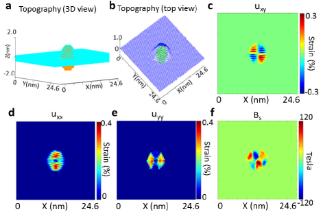
It is interesting to note that the spatial distribution of the strain-induced pseudo-magnetic fields reveals an approximate three-fold symmetry pattern with alternating polarity of values that maximize around the location of the gold nanoparticle. The orientation of the three-fold symmetry pattern coincides with the zigzag direction of the graphene lattice structure, suggesting that the alignment of the nanoscale structural distortions relative to the crystalline lattice of graphene is an important parameter in the strain engineering of graphene. We further note the large magnitude of values (up to Tesla, Fig. 5f), suggesting substantial modifications of the graphene electronic properties under such a nanostructure of comparable lateral and vertical dimensions. For comparison, if the maximum height is reduced from 2.4 nm to 1.2 nm, the maximum value decreases from to Tesla, which is consistent with the strong dependence of the induced strain on the aspect ratio of the building block.
III.3 Theoretical results due to strain induced by two identical nanostructures on the substrate
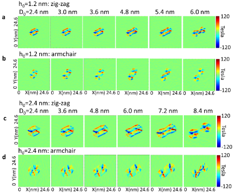
In order to better understand the effects of nanostructure alignment relative to the graphene crystalline lattice and the correlation of strain induced by separate nanostructures, we examined the spatial maps of due to two identical nanospheres and two identical nano-hemispheres aligned relative to either the zigzag or the armchair direction and under varying separations between the centers of the two nanoparticles. As shown in Fig. 6a-b, for two hemispheres of nm diameter and nm, the resulting pseudo-magnetic field for particle alignment along the zigzag direction appears to exhibit stronger correlation than along the armchair direction. In particular, for the nanoparticle separation , nearly uniform stripes of pseudo-magnetic fields appeared along the zigzag direction, with alternating polarities of maximal values extending over nearly equal widths ( nm) perpendicular to the zigzag direction (Fig. 6a). In contrast, insignificant spatial correlation was found for the nano-hemispheres aligned along the armchair direction for all appreciable values, as shown in Fig. 6b.
For comparison, the distributions induced by two nanospheres (Fig. 6c-d) with nm also revealed stronger spatial correlation along the zigzag direction. However, in contrast to the nearly equal widths of alternating pseudo-field polarities in Fig. 6a with nm, the widths of alternating polarities of maximal values are not equally spaced so that substantial regions of the strained areas are covered by relatively smaller values. On the other hand, the spatial correlation of the pseudo-magnetic fields between the two nanoparticles appears to be more extended for nm than that for nm, suggesting that a larger degree of z-axis distortion in graphene also induces a longer range of lateral strain.
III.4 General strategies for simulating arrays of nano-structures
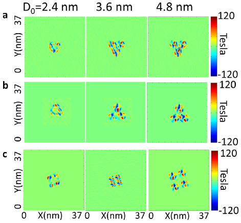
In addition to linear alignments of the building blocks of nano-spheres and nano-hemispheres, we examined different arrangements of the building blocks, such as three nano-spheres arranged in an equal triangular shape shown in Fig. 7a and 7b for each two nano-particles aligned along the zigzag and armchair directions, respectively; and for four nano-particles arranged in a squared shape shown in Fig. 7c for each two nano-particle aligned along alternating zigzag and armchair directions. In contrast to the findings in Fig. 6 where significant differences are apparent between nanostructures along the zigzag and the armchair directions, both types of triangular arrangements in Fig. 7a and 7b appear to be quite similar, with one side of the triangular arrangement differing from the other two sides. This finding is analogous to the three-fold symmetry breaking situation of the Kekule distortion. 16 Furthermore, for the squared-shape arrangement of nanoparticles along alternating zigzag and armchair directions, there is no apparent correlation of the pseudo-magnetic field pattern along any one side of the square, suggesting a frustrated configuration.
Finally, we consider the pseudo-magnetic field distributions induced by ridge-like nanostructures aligned along either the zigzag or the armchair directions, as exemplified in Fig. 8a for the topography four nano-hemispheres of an identical diameter 2.4 nm. The maps of distributions over an area of nm2 for the nano-hemispheres aligned along the zigzag direction for inter-particle separations of 2.4, 3.6 and 4.8 nm are shown in Fig. 8b, and those for nano-hemispheres aligned along the armchair direction are illustrated in Fig. 8d. We find that for sufficiently closely spaced nano-hemispheres aligned along the zigzag direction, nearly uniform and stripe-like distributions of pseudo-magnetic fields could develop along the zigzag direction while the polarity of the pseudo-magnetic fields would alternate over nm width perpendicular to the zigzag direction. As exemplified in Fig. 8c for the height () and the pseudo-magnetic field () distributions along the white line shown in the middle panel of Fig. 8b for nm, we find that the value correlates closely with and maintains relatively large values ( Tesla) except near the two ends of the nano-hemisphere distributions. In contrast, the pseudo-magnetic fields along the armchair direction tend to alternate in polarity more rapidly and so could not form extended regions of uniform pseudo-magnetic fields (Fig. 8d).
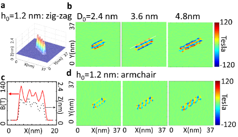
Based on the findings in Fig. 8, we expect that a ridge with a constant height and a constant slope would be able to produce relatively uniform values within an extended spatial width ( nm) and alternating in sign across the lateral direction normal to the zigzag axis.
IV Experimental approaches to nano-scale strain engineering
As discussed previously, our new PECVD approach to graphene growth can reproducibly fabricate nearly strain-free and large-area monolayer graphene with excellent properties, hence suitable for use in strain engineering. In this section we describe our empirical attempts to achieve controlled strain in initially strain-free graphene and demonstrate preliminary proof-of-concept results.
IV.1 Engineering arrays of nanodots on silicon substrates by focused-ion-beam and electron-beam lithography
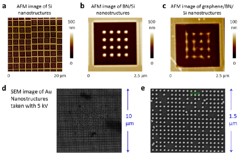
Our first step towards nanoscale strain engineering of graphene was to investigate whether initially strain-free graphene could conform well to periodic arrays of nanostructures and would result in significant strain and pseudo-magnetic fields as theoretically predicted. To this end, we fabricated periodic spherical nanostructures using a dual focused ion beam (FIB) and scanning electron microscope (SEM) (FEI Nova NanoLab™ 600 DualBeam). The primary Ga+ ion beam was operated at 30 keV and beam current was 10 pA. After the fabrication, we determined the topography of these nanostructures by means of both SEM and atomic force microscopy (AFM). The SEM images were taken with 5 kV acceleration voltage, 98 pA beam current, and a working distance mm. The AFM images were acquired in the tapping mode by Bruker Dimension Icon AFM.
The nanostructures that we fabricated on silicon using the Ga-FIB consisted of nanodots with a diameter of nm and a height of nm, as shown in Fig. 9a. These nanostructures were repeated into arrays with an average separation of nm (between the centers of two neighboring nanodots) within a square, and the same arrangements were repeated over a area. Monolayer hexagonal boron nitride (h-BN) was then transferred onto the Si-nanostructures, followed by the transfer of PECVD-graphene onto the substrate of BN/Si-nanostructures. We performed AFM and SEM measurements on every step of the process, and found that BN conformed very well to the Si-nanostructures, as exemplified by the AFM image in Fig. 9b. Interestingly, upon the deposition of graphene on BN/Si-nanostructures, we found that graphene appeared to wrinkle up slightly along the nanostructures, as exemplified by the AFM image in Fig. 9c. This situation is analogous to our findings from the MD simulations, which revealed the appearance of graphene wrinkles along the alignment of its underlying nanostructures if the nanostructures were not too far apart.
Another approach to construct regular arrays of nanostructures was the use of electron-beam lithography. Specifically, we wrote regular arrays of nanodot sturctures on silicon substrates coated with PMMA. After development and metal deposition, the PMMA was lift-off, thus forming arrays of gold nanodots, as exemplified in Fig. 9d-e for a typical nanodot diameter and inter-dot separation of nm. The advantage of using electron-beam lithography to Ga-FIB is the ability of making a much larger area of the same density of the nanostructures by using masks, which is in contrast to the slow process of writing individual nanodots by the FIB. On the other hand, special care must be taken to ensure that gold nanoparticles remain in position throughout the placement of h-BN and graphene.
IV.2 Raman spectroscopic studies of the nanostructure-induced strain effects on graphene
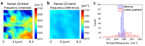
To investigate the macroscopic strain induced by regular arrays of nanostructures, we performed spatially resolved Raman spectroscopic studies on the graphene/BN/Si-nanostructure sample shown in Fig. 9c, and also compared the spectra with those taken from reference areas of the same sheet of graphene without underlying Si-nanostructures. The Raman spectrometer used a laser excitation of 532 nm with a spot size of about 500 nm. We mapped at 0.5 per pixel steps. Each 2D-band spectrum was fit to a single Lorentzian, and the frequency peak position was assigned as the corresponding 2D-band frequency. While the spatial resolution of the Raman spectrometer at 0.5 was not sufficient to resolve the spatial distribution of strain associated with the individual nanodots, it appeared that the strain effects induced by the larger squared features could be resolved in some places. Overall the spatial map of the 2D-band over the area of graphene above the nanostructures clearly revealed significant inhomogeneity (Fig. 10a), which was in sharp contrast to the spatial homogeneity of the 2D-band map of a controlled area of graphene on top of a flat region of the BN/Si substrate (Fig. 10b). A more quantitative comparison of the spatial distributions of the 2D-band frequency in these two areas is illustrated by the histograms in Fig. 10c, where a much broader 2D-band and therefore much wider strain variations induced by the presence of nanostructures is clearly demonstrated.
IV.3 Engineering nanodots on silicon by self-assembly of gold nanoparticles
In order to investigate the strain distributions with much higher spatial resolution, STM must be employed. However, it is generally very challenging to locate the small patterned area within a relatively large sample area, typically on the order of , under the atomically sharp STM tip. While this issue may be addressed by enlarging the total area of patterned nanostructures, another plausible approach was to distribute metallic nanoparticles over the entire substrate by means of self-assembly. This approach could enable quasi-periodic distributions of nanoparticles with a limited range of diameters. Although not ideal for well controlled strain engineering, the use of self-assembled nanoparticles in place of either FIB or electron-beam fabricated nanostructures could provide preliminary and semi-quantitative verifications for our theoretical designs, and so was worthy of exploration.
For this work, the self-assembled gold nanoparticles were developed from solutions on silicon substrates using block copolymer lithography (BCPL) 24 . The preparation procedure is briefly summarized below.
The solutions were mixed in a Pyrex 5 ml micro volumetric flask that was specifically designed for microchemical work. The glassware was cleaned in aqua regia, rinsed in DI water, followed by ultrasonication, and triple rinsed in DI water followed by mild baking to remove any residual moisture. The copolymer (Polymer Source, Inc.) was the diblock copolymers 25.5 mg of polystyrene (81,000)-block-poly(2-vinylpyridine)(14,200), which was dissolved in 5 ml of ultra-high purity toluene (Omnisolve, 99.9%) and spun vigorously with a Teflon stir bar for four days. The solution was clear. The gold precursor was Gold(III) chloride hydrate (99.999% trace metals basis Aldrich, Inc.), and 14.6 mg were added to the diblock copolymer solution under dry nitrogen and in a darkened environment. The solution was then stirred vigorously for l0 days to insure particle uniformity. The solution remained clear upon stirring, but the color changed to amber.
The gold arrays were formed on mechanical grade silicon (5 x 5) mm without removing the native oxide. The silicon substrate was first blown with dry nitrogen to remove particulates and then subjected to a 100 W oxygen plasma (Technics Inc., Planar Etch) for five minutes to remove any hydrocarbon residue. The substrate was loaded on a spin-coater and held in place with a vacuum chuck. The Au-BCPL solution was dropped onto the silicon substrate so that the entire top surface was covered. The sample remained covered for 30 s before starting the spin process. Samples were spun at 3000 RPM for 60 s. The substrate was removed from the spin-coater and placed in an oxygen plasma for 25 minutes at 100 W, and was subsequently removed from the plasma and baked overnight at 220 ∘C.
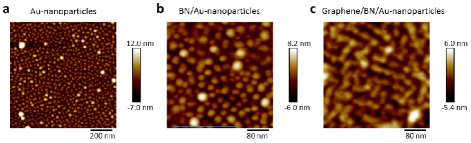
Upon drying the solution and removing the polymer, quasi-periodic gold nanoparticles of diameters ranging from 14 to 20 nm remained and covered the surface of the silicon substrate, with an average separation between adjacent nanoparticles ranging from 10 to 30 nm, as exemplified in Fig. 11a for an AFM image over an area of . Next, a monolayer BN was placed over the Au-nanoparticles/silicon substrate, which was found to conform well to the nanoparticles, as shown in Fig. 11b. Finally, a monolayer PECVD-grown graphene was placed on top of the BN/Au-nanoparticles/silicon, which induced wrinkles on graphene, as illustrated in Fig. 11c and similar to the findings in Fig. 9c. In particular, we note a general preferential wrinkle alignment along approximately 150∘ direction relative to the x-axis of the plot. This preferential direction might be along the zigzag direction of the graphene lattice based on our MD simulations, although further atomically resolved STM studies of the wrinkle structures will be necessary to verify this conjecture.
IV.4 Characterizations of strain-induced modifications to the density of states by scanning tunneling spectroscopy
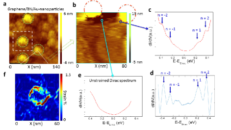
We performed STM and STS studies on the aforementioned graphene/BN/Au-nanoparticle sample at 300 K to characterize the spatial distribution of strain. In Fig. 12a the STM topography over a area revealed the protrusion of graphene above nanoparticle structures. Close-up point spectroscopic studies around the nanoparticle structures (Fig. 12b, which corresponded to the lower left area of Fig. 12a) indicated that in the highly strained regions where maximum changes in the graphene height appeared (with nm descent over a lateral dimension nm), extra spectral features associated with the quantized density of states under a large pseudo-magnetic field appeared on top of the typical Dirac spectrum, as exemplified in Fig. 12c, where the excess quantized spectral features (Fig. 12d, after the subtraction of the Dirac spectrum) correspond to a pseudo-magnetic field Tesla according to Eq. (6). In contrast, for relaxed regions of the graphene sample, the tunneling spectra recovered the standard Dirac spectrum under finite thermal smearing (Fig. 12e). Interestingly, the magnitude of the strain-induced pseudo-magnetic field is somewhat smaller than the result of from the MD simulations for an isolated nano-hemisphere with a diameter 2.4 nm and maximum height nm, the latter having an aspect ratio comparable to that of the Au-nanoparticles used in this work. This finding is reasonable because generally for the same aspect ratio of structural distortions, the induced strain decreases gradually with the increasing physical size of the distortion.
V Discussion
Although the concept of nanoscale strain engineering of initially strain-free graphene samples has been verified semi-quantitatively based on the aforementioned studies, a number of challenges remain.
First, as demonstrated by the MD simulations, the pattern and strength of the pseudo-magnetic field depend strongly on the sizes, shapes, orientations and patterns of the nanostructures on the substrate for graphene. While modern technology for nano-fabrication could manage most of the requirements for the nanostructures, the necessity to align the graphene lattice with high accuracy in orientation relative to the nanostructures is a nontrivial task.
Second, any finite interactions between the substrate material and graphene would complicate the effect induced by generic structural distortions. While our insertion of a monolayer of BN between the substrate and graphene was intended to minimize the influence of the substrate and to preserve the generic properties of graphene, in the event of nearly perfect alignment of graphene with the underlying h-BN lattices, the Dirac electrons of graphene could become gapped 20 so that the theoretical foundation for strain engineering of gapless Dirac fermions would no longer hold.
Third, our MD simulations have assumed perfectly local pseudo-magnetic fields in response to the local strain. This assumption is justifiable if the carrier density in the graphene sheet is sufficiently low so that electronic screening effects are negligible. On the other hand, doping effects of spatially inhomogeneous charged impurities could result in weakened pseudo-magnetic fields and broadened Landau levels, which may account for the relatively broad linewidths observed in the tunneling spectra in Fig. 12c.
Quantitatively, we may incorporate the non-local correction to the evaluation of an effective pseudo-magnetic field at position by following formula:
| (8) | |||||
where denotes the mean free path, and we have assumed that the x-range (y-range) of the sample expands from to (from to ). For a constant pseudo-field distribution over an infinite sample, we have everywhere within the sample as expected. On the other hand, a short mean free path would result in effective values significantly smaller than the local value of according to Eq. (8).
We further remark that the relevant characteristic length involved in the non-local effect of pseudo-magnetic fields in Eq. (8) should be the mean free path rather than the pseudo-magnetic field length , because the contributions from the strain-induced gauge potential are only perturbative to the total Hamiltonian of the Dirac fermions, hence not all Dirac fermions are completely localized to the length scale of by the presence of a pseudo-magnetic field, which is different from the situation for a global time-reversal symmetry breaking magnetic field.
For a given spatial distribution of , if we define the deviation of the effective pseudo-magnetic field from its local value by , we find that from Eq. (6), the linewidth of the Landau level energy becomes . Therefore, the linewidth of increases with increasing non-local corrections to . On the other hand, for a given pseudo-magnetic field distribution we expect sharper Landau levels at locations with larger values. Ultimately, we expect much sharper conductance peaks for pseudo-magnetic fields induced on nearly impurity-free graphene by well ordered and well shaped nanostructures, and hope to verify this notion by further experimental investigation.
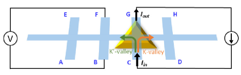
Finally, we note that the presence of pseudo-magnetic fields can lift the degeneracy of the two valleys, which could enable valleytronic applications. As exemplified in Fig. 13, we can in principle detect the valley Hall effect (VHE) in a design similar to that depicted for measurements of the VHE on the graphene/h-BN superlattice structure, 20 except that we do not align the crystalline lattices of graphene and h-BN. Rather, we would use a tetrahedron-shaped nanodot to split the valley currents and employ a backgate to tune the Fermi level to the Dirac point for maximum response. This design is equivalent to a valley field-effect-transistor enabled by the strain-induced topological currents. Moreover, the ability to split the valley degeneracy into two paths with opposite chirality may be utilized in novel designs of either passive devices such as chiral electronics for detectors and light polarizers, or active devices such as tabletop free electron lasers with strain-induced, polarity-alternating pseudo-magnetic fields (see, for example, Fig. 8b) as the undulators for accelerating valley-polarized Dirac fermions into synchrotron radiation.
VI Conclusion and Outlook
We have reviewed in this work the theoretical foundation for nanoscale strain engineering of graphene, and have demonstrated the use of molecular dynamics techniques for designing various nanostructures to realize different patterns of pseudo-magnetic fields. We have also presented experimental evidences for strain-induced charging effects and giant pseudo-magnetic fields, and described feasible empirical approaches based on nano-fabrication techniques to realizing strain-engineering of pseudo-magnetic fields and valleytronics.
While the nanoscale strain engineering effects may be determined by STM, we emphasize that useful designs must ensure that the strain effects are extended to mesoscopic and even macroscopic scales for realistic device applications. Hence, the use of theoretical simulations (such as the molecular dynamics techniques) to assist the design of collective nanostructures for desirable strain distributions and device performance can greatly improve the effectiveness of experimental implementations.
Finally, we remark that the feasibility of nanoscale strain-engineering and valleytronics in graphene is based on the unique electronic properties of this novel nano-material and the availability of modern nanotechnology. With due ingenuity, imagination and diligence, the interesting interplay of structural, electronic and topological properties of nano- and meta-materials is likely to open up new frontiers in scientific and technological exploration that have not been envisioned before.
Acknowledgements.
This project was jointly supported by the National Science Foundation under the Institute for Quantum Information and Matter (IQIM) at California Institute of Technology, a grant from the Northrup Grumman Cooperation, and a gift from Mr. Lewis van Amerongen.References
- (1) Castro Neto, A.H., Guinea, F., Peres, N.M.R., Novoselov, K.S., Geim, A.K.: The electronic properties of graphene. Rev. Mod. Phys., 81, 109–162 (2009)
- (2) Novoselov, K.S., Geim, A.K., Morozov, S.V., Jiang, D., Katsnelson, M.I., Grigorieva, I.V., Dubonos, S.V., Firsov, A.A.: Two-dimensional gas of massless Dirac fermions in graphene. Nature 438, 197 (2005)
- (3) Geim, A.K., Novoselov, K.S.: The rise of graphene. Nat. Mater. 6, 183 (2007)
- (4) Guinea, F., Katsnelson, M.I., Vozmediano, M.A.H.: Midgap states and charge inhomogeneities in corrugated graphene. Phys. Rev. B 77, 075422 (2008)
- (5) Suzuura, H., Ando, T.: Phys. Rev. B 65, 235412 (2002)
- (6) Manes, J.L.: Phys. Rev. B 76, 045430 (2007)
- (7) Guinea, F., Katsnelson, M.I., Geim, A.K.: Energy gaps and a zero-field quantum Hall effect in graphene by strain engineering. Nat. Phys. 6, 30 (2010)
- (8) Guinea, F., Geim, A.K., Katsnelson, M.I., Novoselov, K.S.: Generating quantizing pseudomagnetic fields by bending graphene ribbons. Phys. Rev. B 81, 035408 (2010)
- (9) Teague, M.L., Lai, A.P., Velasco, J., Hughes, C.R., Beyer, A.D., Bockrath, M.W., Lau, C.N., Yeh, N.-C.: Evidence for strain-induced local conductance modulations in single-layer graphene on SiO2. Nano Lett. 9, 2542 (2009)
- (10) Yeh, N.-C., Teague, M.L., Yeom, S., Standley, B.L., Wu, R.T.-P., Boyd, D.A., Bockrath, M.W.: Strain-induced pseudo-magnetic fields and charging effects on CVD-grown graphene. Surface Science 605, 1649–-1656 (2011)
- (11) Levy, N., Burke, S.A., Meaker, K.L., Panlasigui, M., Zettl, A., Guinea, F., Castro Neto, A.H., Crommie, M.F.: Strain-induced pseudo–magnetic fields greater than 300 Tesla in graphene nanobubbles. Science 329, 544 (2010)
- (12) Yeh, N.-C., Teague, M.L., Wu, R. T.-P., Chu, H., Boyd, D.A., Bockrath, M.W., He, L., Xiu, F.-X., Wang, K.-L.: Scanning tunneling spectroscopic studies of Dirac fermions in graphene and topological insulators. EPJ Web of Conferences 23, 00021 (2012)
- (13) Li, X., Cai, W., An, J., Kim, S., Nah, J., Yang, D., Piner, R., Velamakanni, A., Jung, I., Tutuc, E., Banerjee, S.K., Colombo, L., Ruoff, R.S.: Large-area synthesis of high-quality and uniform graphene films on copper foils. Science 324, 1312 (2009)
- (14) Hao, Y. et al.: The role of surface oxygen in the growth of large single-crystal graphene on copper. Science 342, 720 (2013).
- (15) Herbut, I.F.: Pseudomagnetic catalysis of the time-reversal symmetry breaking in graphene. Phys. Rev. B 78, 205433 (2008)
- (16) Araki, Y: Chiral symmetry restoration in monolayer graphene induced by Kekule distortion. Phys. Rev. B 84, 113402 (2011)
- (17) Yeh, N.-C., Teague, M.L., Yeom, S., Standley, B.L., Boyd, D.A., Bockrath, M.W.: Nano-scale strain-induced giant pseudo-magnetic fields and charging effects in CVD-grown graphene. ECS Transactions 35 (3), 161 (2011)
- (18) Rycerz, A., Tworzydlo, J., Beenakker, C.W.J.: Valley filter and valley valve in graphene. Nat. Phys. 3, 172 (2007)
- (19) Lee, M.-K., Lue, N.-Y., Wen, C.-K., Wu, G.Y.: Valley-based field-effect transistors in graphene. Phys. Rev. B 86, 165411 (2012)
- (20) Gorbachev, R.V., Song, J.C.W., Yu, G.L., Kretinin, A.V., Withers, F., Cao, Y., Mishchenko, A., Grigorieva, I.V., Novoselov, K.S., Levitov, L.S., Geim, A.K.: Detecting topological currents in graphene superlattices. Science 346, 448 (2014)
- (21) Boyd, D.A., Lin, W.-H., Hsu, C.-C., Chen, C.-C., Wu, C.-I., Yeh, N.-C.: Single-step deposition of high mobility graphene at reduced temperatures. Nat. Comm. 6, 6620 (2015)
- (22) Ferrari, A.C. et al. Raman spectrum of graphene and graphene layers. Phys. Rev. Lett. 97, 187401 (2006).
- (23) Ferralis, N., Maboudian, R., Carraro C. Evidence of structural strain in epitaxial graphene layers on 6H-SiC(0001). Phys. Rev. Lett. 101, 156801 (2008).
- (24) Boyd, D.A. Block Copolymer Lithography. Chapter 13 in New and Future Developments in Catalysis, edited by Steven L. Suib, Elsevier, Amsterdam, Pages 305-332 (2013). ISBN 9780444538741, http://dx.doi.org/10.1016/B978-0-444-53874-1.00013-5.