MoTe2: A Type-II Weyl Topological Metal
Abstract
Based on the ab initio calculations, we show that MoTe2, in its low-temperature orthorhombic structure characterized by an X-ray diffraction study at 100 K, realizes 4 type-II Weyl points between the -th and +1-th bands, where is the total number of valence electrons per unit cell. Other WPs and nodal lines between different other bands also appear close to the Fermi level due to a complex topological band structure. We predict a series of strain-driven topological phase transitions in this compound, opening a wide range of possible experimental realizations of different topological semimetal phases. Crucially, with no strain, the number of observable surface Fermi arcs in this material is – the smallest number of arcs consistent with time-reversal symmetry.
The ability of gapless band structures to host topological features was first discussed in the context of liquid He Volovik (2009); Bevan et al. (1997). It recently became relevant to crystalline materials with the experimental discovery Lv et al. (2015); Xu et al. (2015) of the theoretically predicted Huang et al. (2015a); Weng et al. (2015a) Weyl semimetals (WSM) in the TaAs family of compounds. In WSMs a topologically protected band crossing of two bands occurs in the close vicinity of the Fermi level forming a gapless node Nielsen and Ninomiya (1983); Murakami (2007); Wan et al. (2011). The low-energy Hamiltonian for such semimetals is that of a Weyl fermion Weyl (1929), which exhibits interesting spectroscopic and transport phenomena such as Fermi arcs Wan et al. (2011); Silaev and Volovik (2012) and the chiral anomaly Nielsen and Ninomiya (1983); Volovik (1986); Xiong et al. (2015); Zhang et al. (2016); Huang et al. (2015b).
It was recently shown Soluyanov et al. (2015) that in materials Weyl fermions come in two flavors: while the type-I Weyl point (WP) (the condensed matter counterpart of the high-energy theory Weyl fermion) is associated with a closed point-like Fermi surface, its newly proposed type-II cousin Soluyanov et al. (2015) appears at the boundary of electron and hole pockets, and has transport properties that are very different from those of the usual, type-I WSM. Another kind of topological metal – a nodal line metal Burkov et al. (2011); Heikkilä et al. (2011); Lu et al. (2013); Weng et al. (2015b); Kim et al. (2015); Xie et al. (2015); Bian et al. (2016); Fang et al. (2015); Yu et al. (2015) – occurs when bands cross along a line in the Brillouin zone (BZ), giving rise to surface states shaped like the surface of a drum Yu et al. (2015). The existence of such a nodal line requires the presence of a symmetry, such as mirror symmetry (or the combination of time reversal and inversion in the absence of spin-orbit coupling (SOC) Wang et al. ), in the material.
A WP is associated with a topological charge, since it represents a sink or source of Berry curvature. A nodal line is associated with a Berry phase of along any mirror-symmetric closed trajectory linking with the line. According to the fermion doubling theorem Nielsen and Ninomiya (1981a, b) the number of sinks in a crystal has to be equal to the number of sources, meaning that WPs can only appear and annihilate in pairs of opposite topological charge. In non-magnetic materials the presence of time-reversal symmetry dictates the minimal number of WPs to be four, giving rise to two Fermi arcs on the surface of the material. The WSMs experimentally discovered Lv et al. (2015); Xu et al. (2015); Arnold et al. (2016) and theoretically predicted Huang et al. (2015a); Weng et al. (2015a); Liu and Vanderbilt (2014); Hirayama et al. (2015); Bzdušek et al. (2015) to date all have more than the minimal number of WPs, as well as a multitude of Fermi arcs, which prevent clean spectroscopy. Of type-I WSMs the TaAs family Huang et al. (2015a); Weng et al. (2015a), hosts 24 WPs and the recently predicted type-II WSM WTe2 hosts 8 of them between the -th and -th bands, where is the total number of valence electrons per unit cell. Below we refer to the bands below band inclusive as valence, and the ones above as conduction.
In search for other type-II WSMs, it is natural to look at compounds chemically similar to WTe2. One such compound, MoTe2 in a previously unreported orthorhombic phase was argued to be a strong candidate for another realization of type-II WSM Sun et al. (2015); Soluyanov et al. (2015). A very recent interesting work Sun et al. (2015) reported that orthorhombic MoTe2 also hosts type-II WPs in the plane between bands and (as WTe2), for the MoTe2 crystal structure measured at 120 K. By further analyzing the MoTe2 structure reported in Ref. Sun et al. (2015), we found that in addition there are 16 WPs out of the plane also formed by bands and , located in the immediate vicinity of the Fermi level 111Two of these points are at ( meV above ) and ( meV above ). Another 6 points are related to these ones by the mirror reflections and , and 8 more points are located symmetrically to these ones about the plane.
In this paper we present the experimental structure of MoTe2 at 100 K and use it to perform first principles and tight-binding calculations of the band structure topology around the Fermi level. Our calculation suggests a different topological physics around the Fermi level than that reported in Ref. Sun et al. (2015): we find only type-II WPs (which we call ) between bands and meV above the Fermi level. These WPs give rise to only 2 clean visible Fermi arcs on the surface of this material. In this sense MoTe2 represents a ”hydrogen atom” of time-reversal invariant WSMs, having the minimal possible number of WPs consistent with time-reversal symmetry. We provide arguments that the difference with the WPs in the plane reported in Ref. Sun et al. (2015) comes from the high sensitivity of the band structure of MoTe2 to even small changes in lattice parameters – MoTe2 lies on a cusp between a transition from to nodes in between valence and conduction bands in the plane. Indeed, there are small differences in the crystallographic data of Ref. Sun et al. (2015) at 120 K and the one reported here at 100 K resulting in the unit cell volume decrease of about 1%, suggesting the possibility of a temperature-driven topological phase transition.
Another recent work Chang et al. (2016) predicts the existence of WPs in Mo doped WTe2. That prediction is obtained by interpolating between the tight-binding models of WTe2 and a theoretically relaxed orthorhombic MoTe2. Such interpolation represents a very strong approximation for the band structure of a doped compound, which, together with the above discussed sensitivity of the WPs to even small differences in the experimental crystal structure, makes the predictions of the work Chang et al. (2016) unreliable. More valuable discussions about strain-driven topological phase transition are presented in the Supplementary Information (S.I.).
Moreover, in metals it is important to look at other topological features near the Fermi level, not only those formed between valence and conduction bands, since the occupation becomes a function of crystal momentum in this case Gosálbez-Martínez et al. (2015), and we find many such additional features in MoTe2. Inspection of crossings between bands other than and , occurring close to the Fermi level, reveals many additional topologically protected crossings formed by the conduction bands and , including line nodes and WPs, some of which (20 in total) are close in energy to the points (see S.I.). We find also two nodal lines close to the Fermi level, formed by the valence bands and , protected by mirror symmetry. Unlike points that are formed at the boundary of electron and hole pockets, the additional topological features arise at the touching points of two pockets of the same carriers. Thus, despite a complex topological band structure, the surface Fermi arcs arising due to the four type-II points are rather clean and should be easy to see in spectroscopic experiments, while the surface states associated with the additional topological crossings overlap with surface projections of the bulk states.
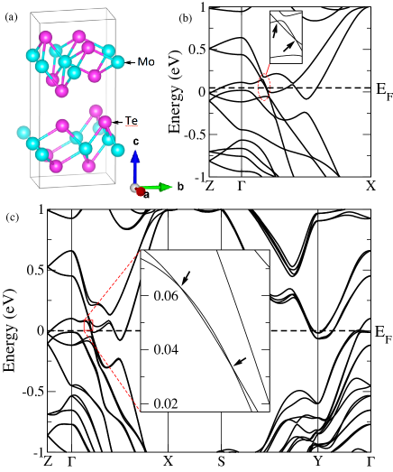
We grew samples by slow cooling and performed diffraction measurements at 100 K. Our results establish that MoTe2 has a new low temperature orthorhombic 1T’-phase (as was previously reported in Sun et al. (2015)), which we designate as the -phase (see S.I. for the full structure characterization). Using this crystallographic data, we perform ab initio calculations based on the density functional theory (DFT) Hohenberg and Kohn (1964); Kohn and Sham (1965) and the generalized gradient approximation (GGA) for the exchange-correlation potential Perdew et al. (1996a). We first compute the band structure of MoTe2 without spin-orbit coupling (SOC), as illustrated in Fig. 1(b). We find 2 mirror-protected nodal lines in the ky=0 plane (more details in S.I.) and 12 WPs formed by valence and conduction bands, 4 of which are located in the plane (W1 points) and 8 are out of that plane (W2 points), as shown in Tab. 1.
The strong SOC of Mo 4- and Te 5-states which dominate the physics around significantly changes the band structure as shown in Fig. 1(c). We first elucidate the topological crossings between valence and conduction bands. The two nodal loops present without SOC become fully gapped. The structure of WPs also changes significantly: the WPs at disappear, while only four WPs are found in the plane, still allowed by the symmetry Soluyanov et al. (2015); Wang et al. (see symmetries in S.I.). The coordinates of these points () are given in Tab. 1. Their location and Chern numbers (see S.I. for the details of Chern number calculation) are illustrated in Fig. 2. The separation between the nearest points with opposite Chern numbers in the unstrained MoTe2 is 10% of the reciprocal lattice constants meaning that the topological Fermi arcs should be easily observable in this material. While, as shown below, other topological gapless features show up very close to the in between bands other than and , it is the WPs that are most important as they give rise to the only Fermi arcs not superimposed on bulk states upon surface projection.
| Weyl points | Coordinates | Chern number | |
|---|---|---|---|
| () | (meV) | ||
| W1 | |||
| W2 | |||
We computed topological invariants to establish the existence of the WPs, and to prove that no additional WPs are present in between the valence and conduction bands. The first invariant is the Chern number, associated with each of the WPs, which was computed both from the Wannier-based tight-binding model Souza et al. (2001); Mostofi et al. (2008), and directly from first-principles calculations Gresch et al. (see S.I.). The result of this calculation is illustrated in Tab. 1 and Fig. 2, where the WPs and their Chern numbers are shown in the BZ.
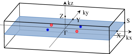
Further insight into the topology of the Bloch bands of MoTe2 is obtained by computing the invariant of the lowest bands on the time-reversal symmetric planes . The plane contains the WPs and is gapless; hence no such invariant can be defined on this plane. The other five planes, however, are gapped between bands and . Of these planes only the one has a non-trivial invariant. This means that the cut of the BZ is analogous to the 2D BZ of a quantum spin Hall insulator that carries an odd number of Kramers pairs of edge states. The lack of a nontrivial invariant on all the other planes implies the existence of disconnected Fermi surfaces. Notice that a connected Fermi sea of the surface states, be it strong or weak topological or trivial insulator, does not lead to only one nontrivial index on a high symmetry plane. Fig. 3 shows the surface spectral function for the -surface of MoTe2, and topological Fermi arcs crossing the plane are clearly visible.
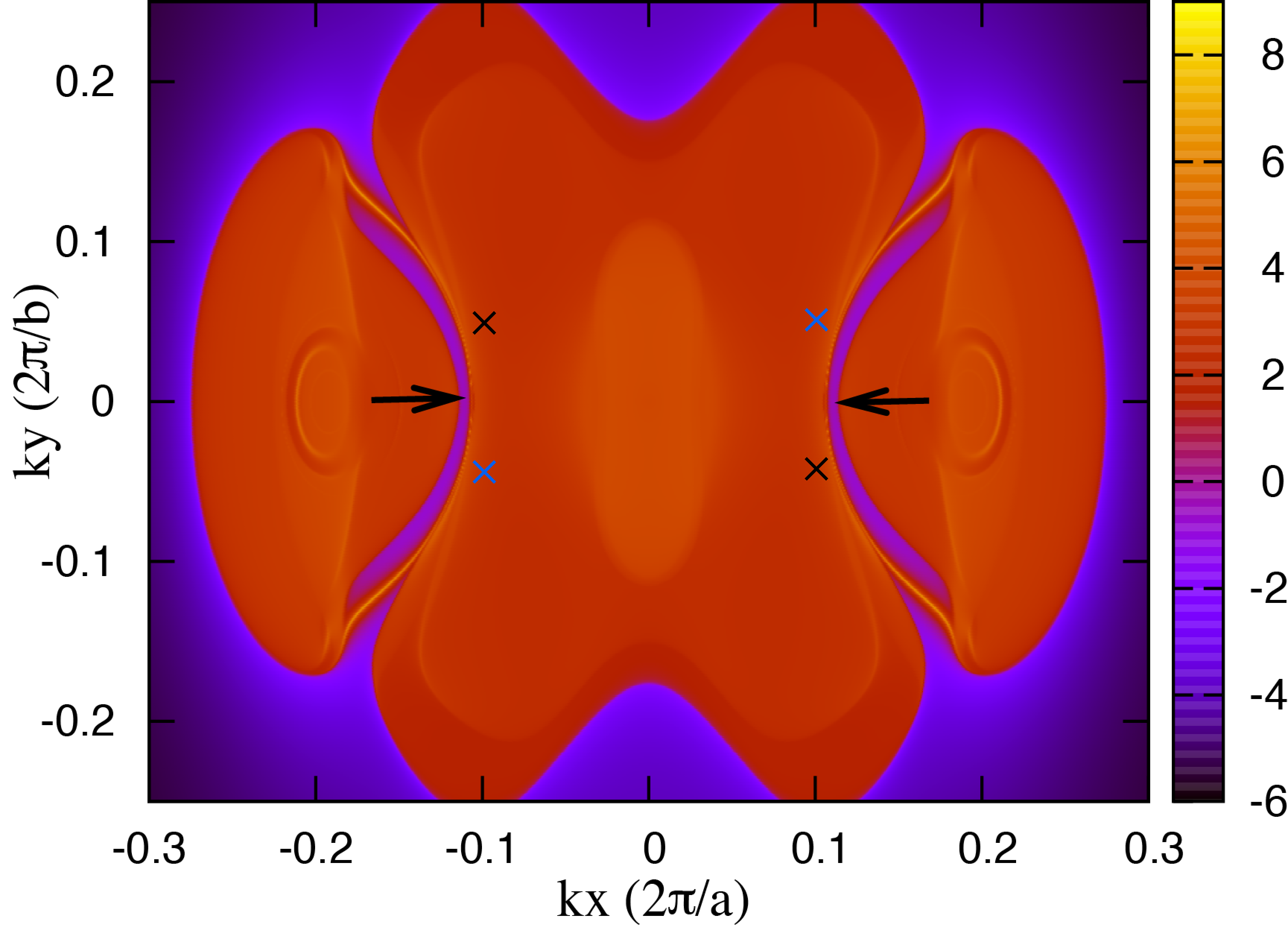
In type-I WSMs tuning the Fermi level to the energy of the WP results in the surface Fermi arcs connecting projections of the WPs on the particular surface. Type-II WPs appear at the boundary between the pockets, when is tuned to the WP energy; hence projections of bulk carrier pockets necessarily appear in the surface electronic density of states irrespective of the Fermi energy in relation to the WP. The Fermi arcs can in this case be hidden within the projection of the bulk pockets on the surface, but they can still be revealed by tuning the chemical potential (see S.I.). This is illustrated for MoTe2 in Fig. 3, where we chose a spectroscopically reachable value for the chemical potential of meV below . The clean Fermi arcs have been revealed in the angle-resolved photoemission spectroscopy measurement Xu et al. (2016). A projection of a big hole-like bulk pocket is seen in the center of the surface BZ, with the projections of the electron-pockets to the left and to the right from it. Unlike the case of type-I WSMs, where a Fermi arc connects surface projections of WPs of opposite chirality, the Fermi arcs illustrated in Fig. 3 are of different nature.
The projections of the WPs are within the projected hole pocket, and all the Fermi pockets have zero Chern numbers, so that in general no Fermi arcs connecting different pockets should appear. However, any cut of the BZ in between two adjacent points () has to exhibit the quantum spin Hall effect, meaning that a Kramers pair of surface states connecting valence and conduction states has to appear in the gap between them, resulting in topological Fermi arcs. Since the arc cannot appear without being connected to projections of WPs or carrier pockets, for it is the topologically trivial state that continues the arc to merge it into the electron pocket (see S.I. for illustrations). The resultant two Fermi arcs represents the cleanest observable consequence of the type-II WPs.
A cross section of the bulk Fermi surface in the plane around the points is illustrated in Fig. 4. The Fermi surface consists of two hole (p) and four electron (n) pockets. The latter form two pairs located to the left (not shown) and to the right (shown) of the p-pockets. When is below the position of the (panel (a)) p- and n-pockets come in pairs of interpenetrating sheets. All the WPs are inside the p-pocket. Upon increasing the p- and n-pockets approach each other and eventually touch at (panel b). Further increase of splits the pockets again, but now is inside the n-pockets (panels c and d). At all times all the pockets have zero Chern number, enclosing an equal number of WPs with opposite chiralities.
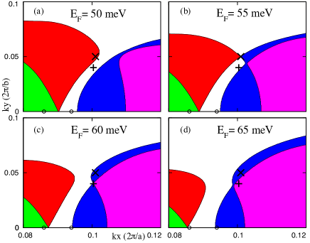
While this concludes the analysis of the WPs between the bands and , MoTe2 exhibits several other topologically protected crossings close to the Fermi level. Even though none of these topological features impact the surface states spectroscopy shown in Fig. 3, as they project inside bulk bands on the surface, we analyze them here for completeness. At only and meV above , two new quartets of WPs exists between the bands and in the plane. One of these points is clearly seen in Fig. 4(c) occurring at the touching points of the two n-pockets. Calculation of additional topological invariants further confirmed the existence of these WPs.
Furthermore, the inset of Fig. 1(c) shows crossings between bands and occurring on the high symmetry line . Symmetry considerations Wang et al. indicate that such crossings on a high-symmetry plane can only occur if a line node is present in the mirror plane of the BZ. Indeed, we find that these bands have different glide plane eigenvalues and two line nodes exist in the plane related by mirror . A further check of the topological nature of this ring is obtained by computing the Berry phase of a loop trajectory that links with the nodal line. We find this to be equal to , as expected for a nodal line.
In conclusion, based on the DFT calculations, we have studied in detail the topological properties of a new orthorhombic -phase of MoTe2, which has been experimentally characterized. The ab initio calculations suggest that unlike the and phases, the -phase hosts a multitude of topological features around the Fermi level including type-II WPs and nodal lines. We found that the WPs between the -th and -th come in a single quadruplet, the smallest number allowed by time-reversal symmetry. This allows for a particularly clean Fermi arc structure on the surface of MoTe2, which should be readily observable in spectroscopic measurements Xu et al. (2016). Other WPs and nodal lines between different other bands also appear in MoTe2, but their spectroscopic signatures on the surface overlap with those of the projected bulk Fermi surfaces.
Acknowledgments We thank Binghai Yan for helpful discussions. This work was supported by NSF CAREER DMR-095242, ONR - N00014-14-1-0330, ARO MURI W911NF-12-1-0461, NSF-MRSEC DMR-0819860, Packard Foundation and Keck grant. D.G., A.S. and M.T. were supported by Microsoft Research, the European Research Council through ERC Advanced Grant SIMCOFE, the Swiss National Science Foundation through the National Competence Centers in Research MARVEL and QSIT. Z.W. and X.D. were supported by the National Natural Science Foundation of China (No. 11504117), the 973 program of China (No. 2013CB921700), and the “trategic Priority Research Program (B)” of the Chinese Academy of Sciences (No. XDB07020100).
References
- Volovik (2009) G. E. Volovik, The Universe in a Helium Droplet (Oxford University Press New York, 2009).
- Bevan et al. (1997) T. Bevan, A. Manninen, J. Cook, J. Hook, H. Hall, T. Vachaspati, and G. Volovik, Nature 386, 689 (1997).
- Lv et al. (2015) B. Q. Lv, H. M. Weng, B. B. Fu, X. P. Wang, H. Miao, J. Ma, P. Richard, X. C. Huang, L. X. Zhao, G. F. Chen, Z. Fang, X. Dai, T. Qian, and H. Ding, Phys. Rev. X 5, 031013 (2015).
- Xu et al. (2015) S.-Y. Xu, I. Belopolski, N. Alidoust, M. Neupane, G. Bian, C. Zhang, R. Sankar, G. Chang, Z. Yuan, C.-C. Lee, et al., Science 349, 613 (2015).
- Huang et al. (2015a) S.-M. Huang, S.-Y. Xu, I. Belopolski, C.-C. Lee, G. Chang, B. Wang, N. Alidoust, G. Bian, M. Neupane, A. Bansil, et al., Nat Comm 6, 7373 (2015a).
- Weng et al. (2015a) H. Weng, C. Fang, Z. Fang, B. A. Bernevig, and X. Dai, Phys. Rev. X 5, 011029 (2015a).
- Nielsen and Ninomiya (1983) H. B. Nielsen and M. Ninomiya, Physics Letters B 130, 389 (1983).
- Murakami (2007) S. Murakami, New Journal of Physics 9, 356 (2007).
- Wan et al. (2011) X. Wan, A. M. Turner, A. Vishwanath, and S. Y. Savrasov, Physical Review B 83, 205101 (2011).
- Weyl (1929) H. Weyl, Zeitschrift für Physik A Hadrons and Nuclei 56, 330 (1929).
- Silaev and Volovik (2012) M. Silaev and G. Volovik, Physical Review B 86, 214511 (2012).
- Volovik (1986) G. E. Volovik, JETP Lett 43, 551 (1986).
- Xiong et al. (2015) J. Xiong, S. K. Kushwaha, T. Liang, J. W. Krizan, M. Hirschberger, W. Wang, R. J. Cava, and N. P. Ong, Science 350, 413 (2015).
- Zhang et al. (2016) C. Zhang, S.-Y. Xu, I. Belopolski, Z. Yuan, Z. Lin, B. Tong, N. Alidoust, C.-C. Lee, S.-M. Huang, H. Lin, et al., Nat. Commun. 7, 10735 (2016).
- Huang et al. (2015b) X. Huang, L. Zhao, Y. Long, P. Wang, D. Chen, Z. Yang, H. Liang, M. Xue, H. Weng, Z. Fang, X. Dai, and G. Chen, Phys. Rev. X 5, 031023 (2015b).
- Soluyanov et al. (2015) A. A. Soluyanov, D. Gresch, Z. Wang, Q. Wu, M. Troyer, X. Dai, and B. A. Bernevig, Nature 527, 495 (2015).
- Burkov et al. (2011) A. Burkov, M. Hook, and L. Balents, Physical Review B 84, 235126 (2011).
- Heikkilä et al. (2011) T. T. Heikkilä, N. B. Kopnin, and G. E. Volovik, JETP letters 94, 233 (2011).
- Lu et al. (2013) L. Lu, L. Fu, J. D. Joannopoulos, and M. Soljačić, Nature photonics 7, 294 (2013).
- Weng et al. (2015b) H. Weng, Y. Liang, Q. Xu, R. Yu, Z. Fang, X. Dai, and Y. Kawazoe, Phys. Rev. B 92, 045108 (2015b).
- Kim et al. (2015) Y. Kim, B. J. Wieder, C. L. Kane, and A. M. Rappe, Phys. Rev. Lett. 115, 036806 (2015).
- Xie et al. (2015) L. S. Xie, L. M. Schoop, E. M. Seibel, Q. D. Gibson, W. Xie, and R. J. Cava, APL Materials 3, 083602 (2015).
- Bian et al. (2016) G. Bian, T.-R. Chang, R. Sankar, S.-Y. Xu, H. Zheng, T. Neupert, C.-K. Chiu, S.-M. Huang, G. Chang, I. Belopolski, et al., Nat. Commun. 7, 10556 (2016).
- Fang et al. (2015) C. Fang, Y. Chen, H.-Y. Kee, and L. Fu, Physical Review B 92, 081201 (2015).
- Yu et al. (2015) R. Yu, H. Weng, Z. Fang, X. Dai, and X. Hu, Phys. Rev. Lett. 115, 036807 (2015).
- (26) Z. Wang, A. A. Soluyanov, J. Li, M. Troyer, and B. Bernevig, in preparation .
- Nielsen and Ninomiya (1981a) H. Nielsen and M. Ninomiya, Nuclear Physics B 185, 20 (1981a).
- Nielsen and Ninomiya (1981b) H. Nielsen and M. Ninomiya, Physics Letters B 105, 219 (1981b).
- Arnold et al. (2016) F. Arnold, C. Shekhar, S.-C. Wu, Y. Sun, M. Schmidt, N. Kumar, A. G. Grushin, J. H. Bardarson, R. D. d. Reis, M. Naumann, et al., Nat. Commun. 7, 11615 (2016).
- Liu and Vanderbilt (2014) J. Liu and D. Vanderbilt, Physical Review B 90, 155316 (2014).
- Hirayama et al. (2015) M. Hirayama, R. Okugawa, S. Ishibashi, S. Murakami, and T. Miyake, Physical Review Letters 114, 206401 (2015).
- Bzdušek et al. (2015) T. Bzdušek, A. Rüegg, and M. Sigrist, Phys. Rev. B 91, 165105 (2015).
- Sun et al. (2015) Y. Sun, S.-C. Wu, M. N. Ali, C. Felser, and B. Yan, Phys. Rev. B 92, 161107 (2015).
- Note (1) Two of these points are at ( meV above ) and ( meV above ). Another 6 points are related to these ones by the mirror reflections and , and 8 more points are located symmetrically to these ones about the plane.
- Chang et al. (2016) T.-R. Chang, S.-Y. Xu, G. Chang, C.-C. Lee, S.-M. Huang, B. Wang, G. Bian, H. Zheng, D. S. Sanchez, I. Belopolski, et al., Nat. Commun. 7, 10639 (2016).
- Gosálbez-Martínez et al. (2015) D. Gosálbez-Martínez, I. Souza, and D. Vanderbilt, Phys. Rev. B 92, 085138 (2015).
- Hohenberg and Kohn (1964) P. Hohenberg and W. Kohn, Phys. Rev. 136, B864 (1964).
- Kohn and Sham (1965) W. Kohn and L. J. Sham, Phys. Rev. 140, A1133 (1965).
- Perdew et al. (1996a) J. P. Perdew, K. Burke, and M. Ernzerhof, Physical review letters 77, 3865 (1996a).
- Souza et al. (2001) I. Souza, N. Marzari, and D. Vanderbilt, Phys. Rev. B 65, 035109 (2001).
- Mostofi et al. (2008) A. A. Mostofi, J. R. Yates, Y.-S. Lee, I. Souza, D. Vanderbilt, and N. Marzari, Computer Physics Communications 178, 685 (2008).
- (42) D. Gresch, A. A. Soluyanov, G. Autés, O. Yazyev, B. A. Bernevig, D. Vanderbilt, and M. Troyer, “Universal Framework for identifying topological materials and its numerical implementation in the Z2Pack software package,” in preparation.
- Xu et al. (2016) N. Xu et al., arXiv preprint arXiv:1604.02116 (2016).
- Brown (1966) B. E. Brown, Acta Crystallographica 20, 268 (1966).
- Vellinga et al. (1970) M. Vellinga, R. De Jonge, and C. Haas, Journal of Solid State Chemistry 2, 299 (1970).
- Ikeura et al. (2015) K. Ikeura, H. Sakai, M. S. Bahramy, and S. Ishiwata, APL Materials 3, 041514 (2015).
- Sheldrick (2000) G. Sheldrick, Inc., Madison, Wisconsin, USA (2000).
- Sheldrick (2008) G. M. Sheldrick, Acta Cryst. A64, 112 (2008).
- Blaha et al. (2001) P. Blaha, K. Schwarz, G. Madsen, D. Kvasnicka, and J. Luitz, wien2k (Technical Universität Wien Austria, 2001).
- Schwarz et al. (2002) K. Schwarz, P. Blaha, and G. Madsen, Computer Physics Communications 147, 71 (2002).
- Perdew et al. (1996b) J. P. Perdew, K. Burke, and M. Ernzerhof, Phys. Rev. Lett. 77, 3865 (1996b).
- Kresse and Furthmüller (1996) G. Kresse and J. Furthmüller, Computational Materials Science 6, 15 (1996).
- Blöchl (1994) P. E. Blöchl, Physical Review B 50, 17953 (1994).
- Kresse and Joubert (1999) G. Kresse and D. Joubert, Physical Review B 59, 1758 (1999).
- Kane and Mele (2005) C. L. Kane and E. J. Mele, Phys. Rev. Lett. 95, 146802 (2005).
- Soluyanov and Vanderbilt (2011a) A. A. Soluyanov and D. Vanderbilt, Phys. Rev. B 83, 035108 (2011a).
- Soluyanov and Vanderbilt (2011b) A. A. Soluyanov and D. Vanderbilt, Phys. Rev. B 83, 235401 (2011b).
- Yu et al. (2011) R. Yu, X. L. Qi, A. Bernevig, Z. Fang, and X. Dai, Phys. Rev. B 84, 075119 (2011).
- Wang et al. (2012) Z. Wang, Y. Sun, X.-Q. Chen, C. Franchini, G. Xu, H. Weng, X. Dai, and Z. Fang, Phys. Rev. B 85, 195320 (2012).
- King-Smith and Vanderbilt (1993) R. D. King-Smith and D. Vanderbilt, Phys. Rev. B 47, 1651 (1993).
- Sancho et al. (1985) M. L. Sancho, J. L. Sancho, J. L. Sancho, and J. Rubio, Journal of Physics F: Metal Physics 15, 851 (1985).
- Note (2) Approximate values of strains are given.
- Note (3) For a strain of % the point moves to .
- Momma and Izumi (2011) K. Momma and F. Izumi, Journal of Applied Crystallography 44, 1272 (2011).
- Williams et al. (2011) T. Williams, C. Kelley, et al., URL: http://www.gnuplot.info (2011).
- Ramachandran and Varoquaux (2011) P. Ramachandran and G. Varoquaux, Computing in Science & Engineering 13, 40 (2011).
- Hunter (2007) J. D. Hunter, Computing In Science & Engineering 9, 90 (2007).
- Gimp (2008) G. Gimp, User manual, Edge-detect filters, Sobel, The GIMP Documentation Team (2008).
- Albert et al. (2013) M. Albert, J. Andler, T. Bah, P. Barbry-Blot, J. Barraud, B. Baxter, et al., “Inkscape,” (2013).
SUPPLEMENTARY INFORMATION
Appendix A Crystal structure of MoTe2
To obtain the low temperature crystal structure of MoTe2 we grew samples by slow cooling and performed diffraction measurements at 100 K to obtain the lattice constants, lattice space group, and atomic coordinates.
A.1 The crystal structure of orthorhombic MoTe2
The crystal structure of orthorhombic MoTe2, the 1T’ form, was determined experimentally at 100 K by single crystal X-ray diffraction. This is a so far (with the exception of the very recent paper of RefSun et al. (2015)) uncharacterized structure for MoTe2, whose crystal structure has been reported previously for a hexagonal symmetry phase (the form), 2H MoTe2, and a monoclinic symmetry phase (the form), 1T” MoTe2 Brown (1966); Vellinga et al. (1970); Ikeura et al. (2015). The crystal structure of the previously reported monoclinic form is related to the structure of orthorhombic WTe2 Brown (1966), but is distorted and therefore is not isostructural with it. Thus, the orthorhombic 1T’ form of MoTe2 characterized here, isostructural with orthorhombic WTe2, is the third characterized structural variant of MoTe2 known; it therefore can be designated alternatively as the phase.
A.2 Experimental details
The crystals of orthorhombic MoTe2 were made by slow cooling (at 1.5 K/hr) a Te-rich flux (95 % Te) from 1000 C to 820 C and then centrifuging off the flux. They were then annealed in a sealed evacuated quartz tube for 12 hours in a thermal gradient, with the crystals at 400 C and the cold end of the tube at about 60 C.
Single-crystal data were collected at 100 K on a Bruker Apex II diffractometer with Mo K (=0.71073 Å) radiation. Data were collected over a full sphere of reciprocal space with 0.5∘ scans in with an exposure time of 30 s per frame. The SMART software was used for data acquisition. Intensities were extracted and corrected for Lorentz and polarization effects with the SAINT program. Numerical absorption corrections were accomplished with XPREP which is based on face-indexed absorption Sheldrick (2000). With the SHELXTL package, the crystal structure was solved using direct methods and refined by full-matrix least-squares on F2 Sheldrick (2008). The largest peak in the final F map was 4.91 eÅ-3, 1.03 Åfrom Te1, and the largest hole was -3.94 eÅ-3, located 0.98 Åfrom Mo1. The crystal refinement and atomic parameters are given in Tabs. 2-3.
| Refined Formula | MoTe2 |
|---|---|
| F.W. (g/mol) | 351.14 |
| Space group; | (No.31); 4 |
| a(Å) | 3.4582(10) |
| b(Å) | 6.3043(18) |
| c(Å) | 13.859(4) |
| V(Å3) | 302.1(2) |
| Absorption Correction | Numerical |
| Extinction Coefficient | None |
| range (deg) | 3.55-29.566 |
| No. reflections | 2765 |
| No. independent reflections | 899 |
| No. parameters | 38 |
| ; (all ) | 0.0579; 0.1223 |
| Goodness of fit | 1.004 |
| Diffraction peak and hole (e-/Å3) | 4.913; –3.941 |
| Atom | Wyckoff. | Occupancy | ||||
|---|---|---|---|---|---|---|
| Mo(1) | 2 | 1 | 0 | 0.0297(6) | 0.7384(6) | 0.012(2) |
| Mo(2) | 2 | 1 | 0 | 0.6062(7) | 0.2240(7) | 0.014(2) |
| Te(1) | 2 | 1 | 0 | 0.2163(8) | 0.1269(5) | 0.015(2) |
| Te(2) | 2 | 1 | 0 | 0.6401(8) | 0.8363(5) | 0.012(2) |
| Te(3) | 2 | 1 | 0.5 | 0.1374(8) | 0.8783(5) | 0.014(2) |
| Te(4) | 2 | 1 | 0.5 | 0.7090(9) | 0.0827(5) | 0.010(2) |
A.3 Symmetries of the -phase
The crystal structure of -MoTe2 with 4 formula units in the unit cell is shown in Fig. (1) in the main text. The corresponding point group is and there are three symmetry operations: the symmorphic reflection , the non-symmorphic reflection , and the non-symmorphic rotation. The translation accompanying the two non-symmorphic operations is in units of the lattice constants. Crucially, in the plane a little group exists at each point formed by the product of time-reversal and , . It is shown in Ref. Soluyanov et al. (2015); Wang et al. that this symmetry allows (just like in WTe2) for the presence of WPs in the plane.
Appendix B Details of numerical calculations
The electronic structure calculations have been carried out using the all-electron WIEN2K package Blaha et al. (2001); Schwarz et al. (2002). A mesh and the exchange-correlation functional with a generalized gradient approximation (GGA) parametrized by Perdew, Burke, and Ernzerhof (PBE) have been used Perdew et al. (1996b).
The results for the electronic band structure and topological invariants were verified versus the pseudopotential calculations done in VASP Kresse and Furthmüller (1996), using PAW Blöchl (1994); Kresse and Joubert (1999) pseudopotentials with and valence electron configurations for Mo and Te, respectively. Spin-orbit coupling was included in the pseudopotentials, and the PBE approximation Perdew et al. (1996b) was used. Self-consistent field calculations were performed on a -centered grid, with a Gaussian smearing of width eV. The energy cut-off was chosen at eV. Additional calculations were done using a -centered grid, with an energy cut-off of either or eV, and also using a Gaussian smearing width of eV. The experimental lattice parameters listed in Tabs. 2-3 are used in the calculations. To calculate the surface states, Wannier functions based tight-binding models for Mo and Te orbitals have been constructed Souza et al. (2001); Mostofi et al. (2008). The topological invariants were verified with both tight-binding and ab initio calculations, where the Z2Pack Gresch et al. (http://z2pack.ethz.ch/doc) package was used for the latter.
Appendix C Band structure in the absence of spin-orbit coupling
The band structure of MoTe2 exhibits several topological features in the absence of spin-orbit coupling (SOC). A clear band inversion and multiple band crossings are found in the band structure around along the line, which is part of the mirror plane. We find that the two bands , (spin is not taken into account) cross along the line, having opposite glide-plane eigenvalues . Theoretical symmetry analysis Wang et al. dictates the appearance of a line node in the plane in case of a degeneracy on the line. Indeed, in this plane we find two nodal lines, related by . The degeneracy point found on the line belongs to one of these nodal lines. In addition, 12 WPs between the and bands are found in MoTe2 in the absence of SOC. Four of these points are located in the plane, while the other eight appear off-plane as two quartets, symmetrically located about . One in-plane point W1 and two out of plane points W2, are listed in Tab. I of the main text, with the other 9 points related to these by and .
Appendix D Weyl points between bands and
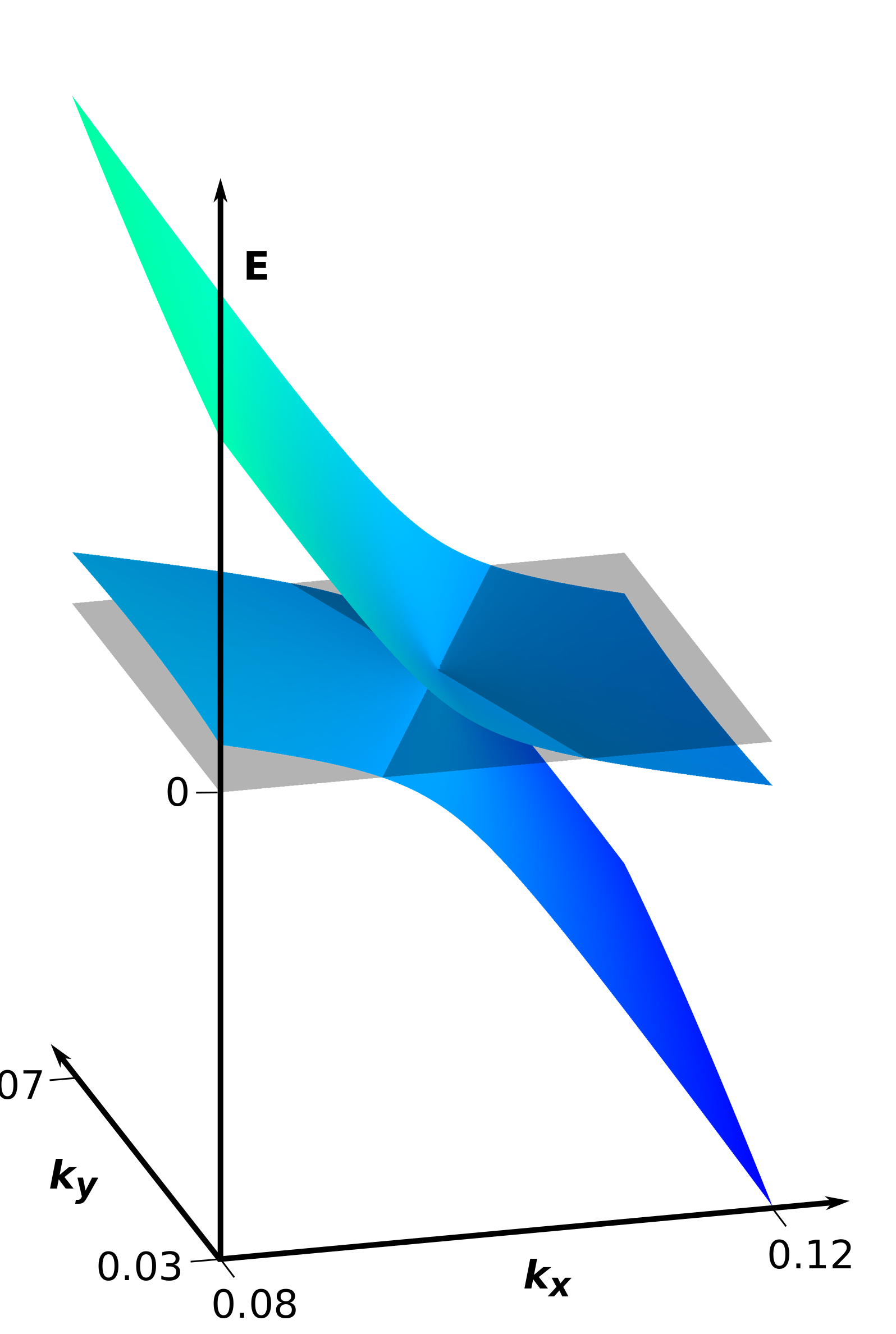
As described in the main text, there are 4 Weyl points (called in the main text) formed by bands and in MoTe2 for the structure reported in this paper. The number corresponds to the number of valence electrons per unit cell. These points are of type-II, as can be seen from the band dispersion obtained from first-principles calculations. The dispersion for the linearized Hamiltonian is illustrated in Fig. 5 clearly showing the Weyl point at the boundary between electron and hole pockets. A general type-II WP Soluyanov et al. (2015) Hamiltonian is written in terms of the Pauli matrices and a kinetic term described by a unit matrix
| (1) |
where there exists a cone of directions in -space, in which the first (kinetic) term of the Hamiltonian dominates over the second (potential) one, that is . Fitting the theoretical model derived from the symmetry analysis to the band structure around the WPs obtained from ab initio calculations results in the following effective Hamiltonian for the WP
| (2) |
with parameters (in eVÅ) , , , , , and . Since there is a direction around which the kinetic energy dominates (), is a type-II WP. If we limit our analysis to the bands and forming only WPs, then MoTe2 would be the simplest possible example of a TR-symmetric type-II WSM.
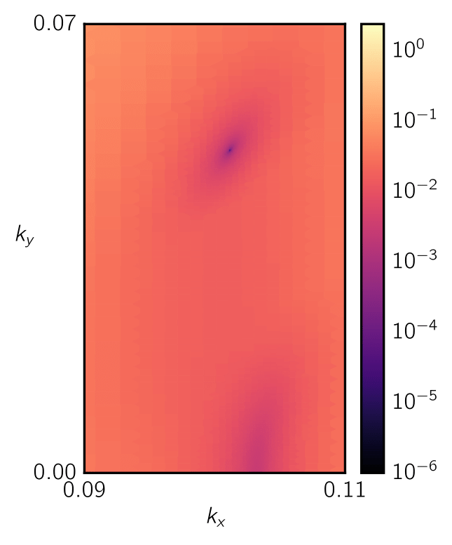
The previous study of Ref. Sun et al. (2015) only considered crossings of bands and and reported 8 type-II Weyl points in MoTe2 in the plane. This discrepancy arises due to the difference in the lattice parameters. Although the difference is small, the 100 K crystal structure reported here is close to the topological phase transition point, where additional Weyl points appear in pairs of opposite chirality from the mirror plane. This can be seen in the Fig. 6, where the gap between the bands and is plotted in the region of interest for cut of the Brillouin zone.
A minor change in the lattice constants can give rise to 4 additional type-II Weyl points in the plane, as illustrated schematically in Fig. 7.
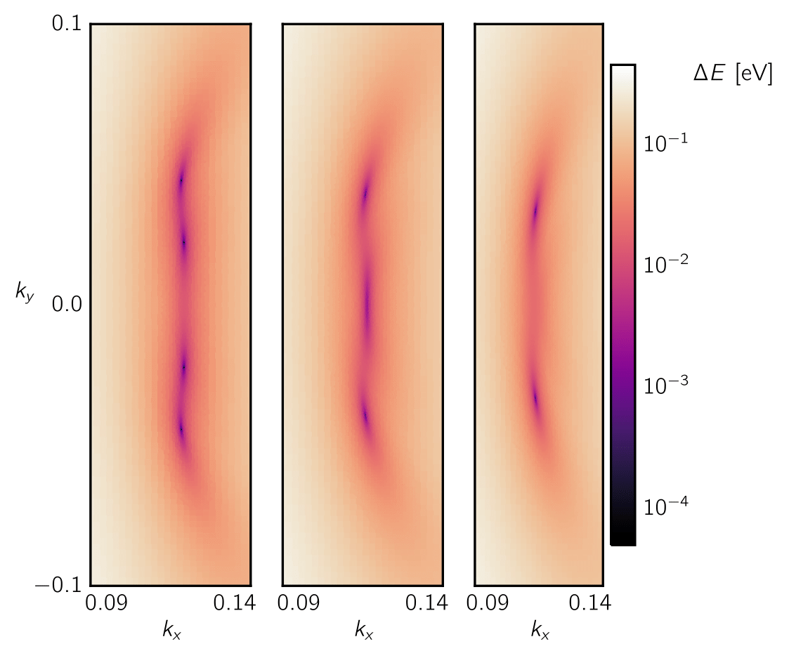
Extreme sensitivity of band structure topology in MoTe2 and the fact that the results of Ref. Sun et al. (2015) are obtained for the different temperature structure suggest the possibility of temperature-driven topological phase transitions in this material.
Appendix E Invariants and their Relation to Weyl points
We establish a connection between invariants used for insulators and the existence of Weyl points. If the usual invariant is nonzero only on one out of the common high-symmetry time-reversal symmetric (TR) planes ( and ), the system has to exhibit Weyl points. This is easy to see. Consider the TR planes shown in the upper left panel of Fig. 8. Let only one of the planes be non-trivial, so that it exhibits a quantum spin Hall effect. The edge modes of the quantum spin Hall effect on this plane can result from (a) a closed surface Fermi surface such as in a weak or strong topological insulator or (b) from a disconnected open surface Fermi surface such as the Fermi arcs. Case (a), however, would imply the existence of another nontrivial index on one of the other TR planes (either parallel or perpendicular to the non-trivial one), hence the only possibility is that of an open Fermi arc surface state. This exercise also reveals the canonical connection pattern between Weyl points on the surface: the Fermi arcs will form the continuation of the quantum spin Hall edge states off the high-symmetry plane.
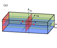
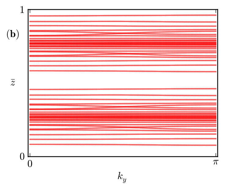

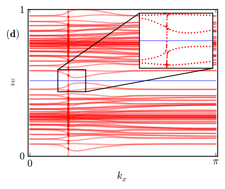
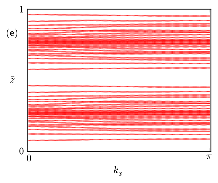
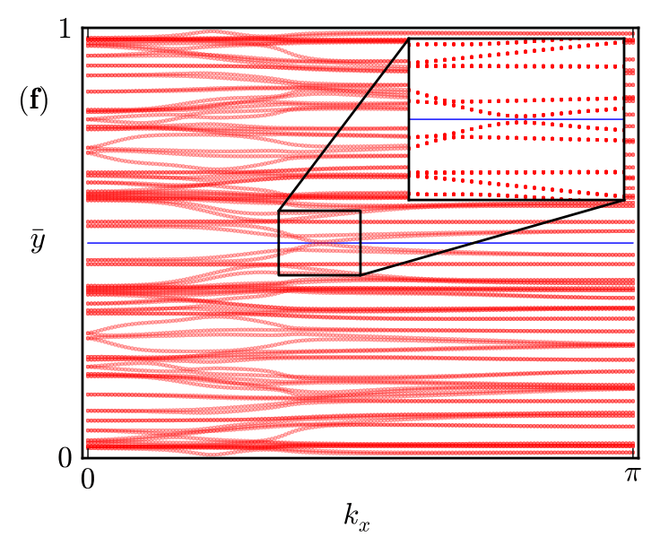
In MoTe2 the valence bands and the conduction bands ( and th bands) are directly gapped on five out of six TR planes, with the exception of the plane that hosts four Weyl points. The appearance of Weyl points and the connection of Fermi arcs can be deduced by analyzing the invariants Kane and Mele (2005) for the these five TR planes. Fig. 8 shows the flow of Wannier centers Soluyanov and Vanderbilt (2011a, b); Yu et al. (2011) on the five planes as calculated directly from first-principles calculations Gresch et al. . All but the planes are trivial, so that the quantum spin Hall effect appears only in the -plane, guaranteeing that non-trivial surface states exist and cross the axis on the surface in accord with the surface state calculation illustrated in Fig. 10 below.
Appendix F Topological charge of Weyl points
Using the crystal symmetry , we only need to calculate the topological charge of the Weyl points within one-fourth of the entire Brillouin zone. The topological charge of a Weyl point can be defined as the net flux of the Berry gauge field penetrating a 2D surface Wan et al. (2011); Wang et al. (2012); Soluyanov et al. (2015)
| (3) |
where the integrand is the Berry connection for the Bloch states calculated on the surface that encloses the Weyl node. By Stokes theorem, the defined above should be equal the topological charge of the Weyl point.
For this reason, the closed Fermi surface of the type-I Weyl point has nonzero topological charge. In the case of a type-II Weyl point, however, the Fermi surface is open, and hence cannot be used to compute the topological charge of the Weyl point. Instead, we integrate the Berry curvature computed for lowest bands, where is the number of electrons per unit cell. A closed surface, on which the lowest states are separated by an energy gap from the other higher energy states, and which encloses the type-II Weyl, can easily be found. This surface defines a 2D manifold in 3D momentum space, formed by the lowest states, and unlike any possible Fermi surface, it corresponds to different energy values for different momenta in the Brillouin zone.
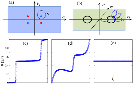
Using both, first-principles calculations and Wannier-based tight-binding models Souza et al. (2001); Mostofi et al. (2008), Bloch states were calculated on spheres enclosing Weyl points. One of such spheres enclosing the point of the main text is shown as a circle in the plane of the Brillouin zone in Fig. 9(a). For the calculation of the topological charge of Weyl points formed by bands and the Berry curvature is computed for bands and the integration surface is chosen such that an energy gap between and bands is present everywhere on it. For further illustration of the topological charge, following the work of Ref. Soluyanov et al. (2015) in Fig. 9(c-d) we plot the total electronic polarization King-Smith and Vanderbilt (1993) for one-dimensional circular cuts of the sphere taken for different values of the polar angle for the Weyl points and one of the points formed between bands and located at . The shift of polarization value when going from to gives the Chern number (chirality) of the Weyl point.
To prove the existence of the line nodes formed by bands and , we calculated the Berry phase acquired by bands along a loop in -space linked with one of the nodal lines, as shown if Fig. 9(b). On each of such loops a gap between bands and exists, so that the Berry phase for the manifold of bands is a well-defined quantity. In the presence of a monopole inside the loop, this Berry phase has to be equal to . As illustrated in Fig. 9(c), all loops have Berry phase thus proving the existence of the line node (that is, a monopole exists within every loop).
Pierced by a line on which the bands and are degenerate, while being gapped on the loop and due to the presence of the mirror plane this Berry phase is equal to as illustrated for a set of loops in Fig. 9(e).
F.1 Weyls and Nodal Lines formed by bands other than and
We found a plethora of topological features formed by bands and , including line nodes on the mirror planes and several sets of Weyl points. Of these the ones found at , , , and (and their mirror images) are of the most relevant located only , , and meV above the Fermi level. Hidden inside the carrier pockets these additional Weyl points and their associated Fermi arcs overlap with the bulk states when projectod onto the experimentally relevant -surface. The nodal lines present on the and planes (including the one formed by bands and ) also do not contribute visible spectroscopic signatures to this surface – their associated drum-head surface states Yu et al. (2015) are projected onto the surfaces other than .
Appendix G Fermi arcs and surface states
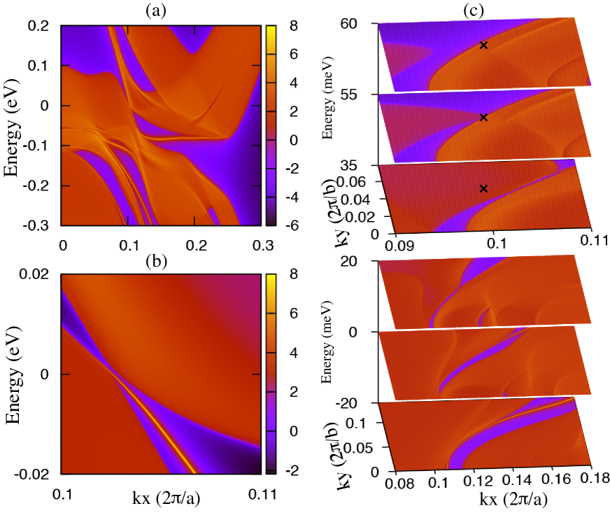
Implementing the Green’s function method of Ref. Sancho et al. (1985) to the Wannier-based tight-binding Hamiltonian generalted from the first-principles calculation, we obtained the surface states for the -surface. They are plotted in Fig. 10, together with the corresponding surface Fermi surfaces. As discussed above, the Weyl points formed by bands and are responsible for the presence of visible surface states in the bulk gapped region. In accord with the discussion above, the surface states connecting valence and conduction states along the direction are clearly seen in the spectral function of the -surface of Fig. 10(a-b).
The connectivity patterns of the corresponding Fermi arcs for the -surface at different energies are shown in Fig. 10(c). Since MoTe2 is a type-II Weyl semimetal, the Fermi arcs are always accompanied by the projections of bulk electron and hole pockets. This makes it possible to tune the Fermi arcs by changing the position of the chemical potential, and Fig. 10(c) illustrates the evolution of the Fermi arc states for different values of the chemical potential. The states are clearly visible when this value is set to meV below the Fermi level.
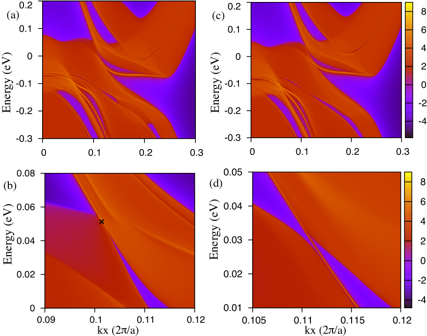
Unlike the case of type-I Weyl semimetals, where the Fermi arc necessarily connects the projections of the Weyl points onto the Fermi surface, here it arises out of the generic point in the electron pocket and dives back into it, as illustrated in the main text. This arc, however is still topologically non-trivial, as illustrated in Fig. 11. At small values of in between the two points the 2D cut of the Brillouin zone exhibits the quantum spin Hall effect, and the corresponding topological surface state is clearly visible connecting the valence and conduction bands across the gap (see Fig. 10(a-b)). At the position of points, that is for the corresponding 2D cut of the Brillouin zone is metallic but a surface state is still seen below the Weyl point at the boundary of the bulk valence bands projection (Fig. 11(a-b)), but it now reconnects from the valence to conduction states. At the 2D cuts of the Brillouin zone become topologically trivial and a topologically trivial surface state is clearly seen in Fig. 11(c-d). Thus, the Fermi arc of the main text is formed by a topological surface state, resulting from the quantum spin Hall effect at small , and the topologically trivial state at larger serves to connect this in-gap state to the projections of the bulk Fermi pockets.
Appendix H Strains
As mentioned in the main text, the band structure of MoTe2 around the Fermi level is very sensitive to changes in the lattice constant. To illustrate this we studied topological phase transitions occurring between the valence and conduction bands in this material under various strain values (see Supplementary Information). We find that for these bands two additional sets of WPs can appear in MoTe2 with small changes in the lattice constants. The first set consists of 4 type-II WPs in the plane arising in pairs of opposite chirality from the mirror plane and giving 8 total WPs in analogy with WTe2 Soluyanov et al. (2015). This scenario is realized under a hydrostatic strain of 222Approximate values of strains are given. % and uniaxial strains of % and % in and correspondingly. Another set of additional WPs consists of type-II nodes appearing off the plane for a hydrostatic strain of % and for uniaxial strains of % and % in and correspondingly. Finally, both sets appear for a uniaxial strain in the direction of % (only % strain is required to generate the additional set at ), while for negative strains in no new WPs are generated between bands and , but the points move closer to each other 333For a strain of % the point moves to .. The strong dependence of the Weyl physics on the applied strain has also been pointed out in Sun et al. (2015). For their structure, it was also found that strain can induce a type-II to type-I Weyl transition Sun et al. (2015). The calculation of strained structures has been performed as follows. The aim of this study was to look at the stability of different topological phases under small changes in the lattice parameters. Here the strained structures were calculated from first-principles by changing the lattice constants only, without further relaxation. To find the critical values of strains at which the topological phase transitions occur, ab initio calculations were performed for a large number of strained structures and the closing of the band gap at the Weyl nodes was observed. The full analysis including the calculation of topological invariants, however, was done only for specific strain values to confirm the qualitative nature of the phase transitions. The approximate values of critical strains were extracted from these calculations.
The details on the calculation of strained structures are as follows. The aim of this study was to look at the stability of different topological phases under small changes in the lattice parameters. Here the strained structures were calculated from first-principles by changing the lattice constants only, without further relaxation. To find the critical values of strains at which the topological phase transitions occur, ab initio calculations were performed for a large number of strained structures and the closing of the band gap at the Weyl nodes was observed. The full analysis including the calculation of topological invariants, however, was done only for specific strain values to confirm the qualitative nature of the phase transitions. The approximate values of critical strains were extracted from these calculations.