Termination-dependent surface properties
in the giant-Rashba semiconductors BiTe ( = Cl, Br, I)
Abstract
The non-centrosymmetric semiconductors BiTe ( = Cl, Br, I) show large Rashba-type spin-orbit splittings in their electronic structure making them candidate materials for spin-based electronics. However, BiTeI(0001) single crystal surfaces usually consist of stacking-fault-induced domains of Te and I terminations implying a spatially inhomogeneous electronic structure. Here we combine scanning tunneling microscopy (STM), photoelectron spectroscopy (ARPES, XPS) and density functional theory (DFT) calculations to systematically investigate the structural and electronic properties of BiTe(0001) surfaces. For = Cl, Br we observe macroscopic single-terminated surfaces. We discuss chemical characteristics among the three materials in terms of bonding character, surface electronic structure, and surface morphology.
I Introduction
The narrow-gap semiconductors BiTe ( = Cl, Br, I) have attracted considerable interest because of large Rashba-type spin-orbit splittings in their bulk and surface electronic structures Ishizaka ; Eremeev_PRL ; Murakawa , which have been observed by angle-resolved photoelectron spectroscopy (ARPES) Crepaldi_PRL ; Landolt_PRL ; Landolt_NJP ; Sakano_PRL ; Moreschini and magnetotransport measurements Martin ; Bell . The enhanced spin-splitting in these materials is driven by their non-centrosymmetric crystal structure in combination with strong atomic spin-orbit coupling and a negative crystal-field splitting of the topmost valence bands Bahramy_PRB . The latter features have also been predicted to promote a topological insulator phase in BiTeI under application of external pressure Bahramy . The BiTe series does not only host the presently largest known Rashba effect of all semiconductors, it also appears more suitable for possible spin-electronic applications Datta ; Zutic than artificially grown monolayer reconstructions, such as metallic surface alloys, where spin-splittings of similar magnitude can be achieved Ast ; Bentmann ; El-Kareh_PRL ; El-Kareh_NJP .
At the surface, the non-centrosymmetric, layered unit cell of BiTe results in two possible polar terminations Crepaldi_PRL ; Eremeev_NJP ; Landolt_NJP ; Moreschini , Te- and -terminated surfaces, that give rise to n-type or p-type band bending, respectively Crepaldi_PRL . The surface properties may be influenced additionally by defects, as is the case for BiTeI, where bulk stacking faults induce coexisting Te- and I-terminated domains on microscopic length scales as shown by scanning tunneling microcopy (STM) Butler ; Tournier ; Kohsaka ; Fiedler . While the resulting lateral interfaces between surface areas of different terminations may provide interesting new physics Butler ; Tournier , the presence of multiple domains will in most instances be undesirable. For BiTeCl and BiTeBr spatially resolved surface investigations have so far been scarce Yan . In the case of BiTeCl photoemission experiments indicate single-terminated surfaces Landolt_NJP , in contrast to BiTeI, whereas for BiTeBr the situation is unclear. The majority of ARPES studies of BiTe point to similar Rashba-split band structures for all three compounds Sakano_PRL ; Landolt_NJP ; Crepaldi_PRB ; Moreschini , in agreement with theoretical predictions Eremeev_PRL ; Moreschini . However, for BiTeCl the existence of topological surface states has also been claimed based on ARPES Chen and STM Yan .
In this work we present a combined investigation of the surface structural and electronic properties of the BiTe semiconductors. Our STM experiments show that BiTeBr and BiTeCl(0001) display single-domain surfaces with X- or Te-termination. The determined terrace step heights agree with the respective bulk unit cell parameters and X-ray photoemission (XPS) provides depth-dependent chemical information in line with the expected layered atomic structure. The measured core-level binding energies indicate a significant charge transfer from Bi to, both, and Te in agreement with density functional theory (DFT) calculations. We systematically compare the electronic properties of Te- and -terminated surfaces in terms of band bending, surface band structure, work function, atomic defects, and reaction to deposited adsorbate atoms.
II Methods
Our experimental setup is designed for a comprehensive analysis of the geometric and electronic properties in real and reciprocal space as described in Ref. Fiedler . The system allows surface analytics by means of various techniques, i.e. LEED, SPA-LEED, STM, STS, AFM, XPS, work function and ARPES measurements in ultra-high vacuum conditions for the same sample without exposing it to air. Additional high-resolution STM measurements were performed at a separate setup with a low-temperature STM (Omicron LT-STM) at K.
We used a modified sample holder system, which allows to split single crystals in situ and to measure both corresponding surfaces of a cleave without the need to re-glue or to expose the sample to air [see Fig. 1(a)]. Thus, BiTe ( = Cl, Br, I) single crystals were cleaved at room temperature along the (0001) direction at pressures low mbar revealing surfaces of about 2 mm2 mm on each side. A podium smaller than the sample was used to move the surface into the focal point of the electron spectrometer in order to minimize spurious signal from the sample holder.
Submonolayer amounts of Cs were deposited using commercial alkali dispensers (SAES Getters). All experiments were performed at room temperature except for those carried out at the LT-STM.
Tips have been prepared according to Ref. Fiedler . Differential conductance maps are used to obtain spatially resolved information about the sample’s local density of states (DOS). For this purpose a small modulation voltage ( mV) is added to the sample bias and the resulting variation of the tunneling current, , is recorded simultaneously with the topograhic, i.e. constant-current image. STM data were processed with the WSxM software package Horcas .
XPS measurements were done with Al K radiation ( = 1486.6 eV) under a photoelectron emission angle of 60 ∘ in order to enhance the surface sensitivity of the experiment. The X-ray source was not monochromatized and the spectra were satellite-corrected. The energy resolution of the XPS measurements was ca. 1 eV. ARPES data were acquired with a non-monochromatized He discharge lamp with He I radiation ( = 21.2 eV) and at an energy resolution of approximately 25 meV. Work functions were determined from the secondary photoelectron cutoff with the sample held on a positive potential of 9 V. Calibration measurements for Au(111) gave values in line with previous reports Trasatti ; Rusu .
The synthesis of the charges was performed by fusing binary compounds: Bi2Te3 with BiCl3, BiBr3 and BiI3, correspondingly. According to published data Tomokiyo ; Petasch BiTeI and BiTeBr melt congruently at 560 ∘C and 526 ∘C, while BiTeCl shows incongruent melting Petasch at 430 ∘C with a peritectic composition around 11 mol.% Bi2Te3 + 89 mol.% BiCl3. Therefore we have used stoichiometric charge for BiTeI, BiTeBr and melt-solution system with a molar ratio Bi2Te3:BiCl3 = 1:9 for the crystallization of BiTeCl. The synthesis was performed directly in the growth quartz ampoules at a temperature which is 20 ∘C above the melting point. Crystal growth was performed by the modified Bridgman method with rotating heat field CrystEngComm . After pulling the ampoules through the vertical temperature gradient of 15 ∘C/cm at 10 mm/day, the furnace was switched off.
Complementary first-principles calculations were performed within the framework of the density functional theory (DFT) using the projector-augmented-wave (PAW) PAW1 ; PAW2 basis. The generalized gradient approximation (GGA-PBE) PBE to the exchange correlation (XC) potential as implemented in the VASP code VASP1 ; VASP2 was used. The relaxed bulk parameters have been taken into account. The atomic charges were estimated by implementing the Bader charge analysis Bader .
III Results
III.1 Surface morphology and bonding character
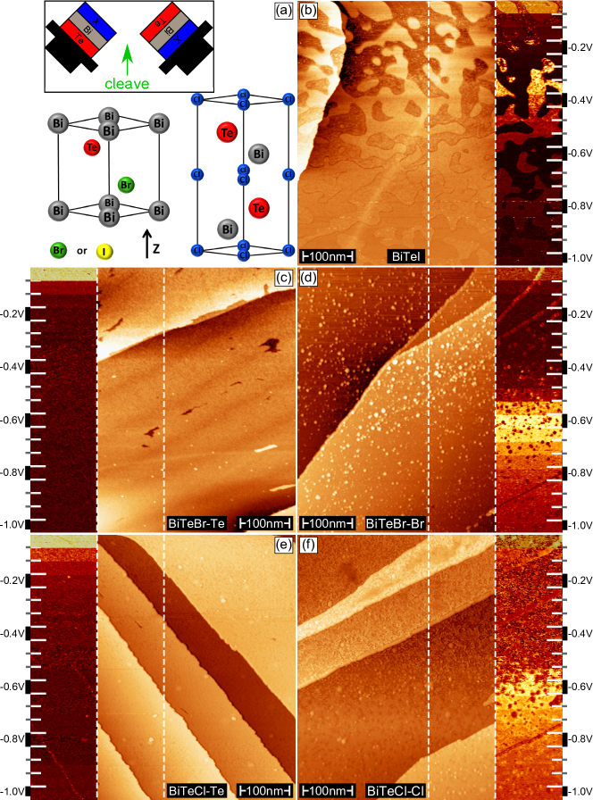
Fig. 1(a) shows the unit cells of BiTe. While BiTeI and BiTeBr have a unit cell of 3 atomic layers, the one of BiTeCl comprises 6 layers along resulting in a height twice as large Eremeev_PRL ; Shevelkov . The inset sketches the stacking order after the cleave of an ideal single crystal, resulting in two different terminations for the two opposing surfaces.
Fig. 1(b) displays a 500 nm500 nm STM measurement of BiTeI(0001) at 0.1 nA tunneling current. During the scan the gap voltage was gradually decreased from -0.05 V at the upper part of the image down to -1.0 V at the lower part. Note that negative voltages refer to tunneling from the sample to the tip, thus reflecting the occupied DOS of the sample as being also accessed by ARPES spectra. Coexisting Te- and I-terminations are visible as reported earlier Butler ; Tournier ; Kohsaka ; Fiedler . The outer part of the image shows the corresponding dI/dV map of the surface within the two white dashed lines. The Te-terminated surface shows a high DOS at -0.05 V while at -0.3 V the same surface appears dark in the dI/dV map and the I-terminated surface reveals a high intensity. This high DOS originates from the onsets of the band structures of the two different terminations, as shown in Ref. Fiedler . The step edges within the same terminations are around 0.7 nm high and the ratio between Te- to I-terminated areas is roughly 50/50.
Next we investigate the surface morphologies of BiTeBr and BiTeCl [see Figure 1(c)-(f)]. The images reflect a surface area of 500 nm500 nm, and were obtained at 0.2 nA tunnelling current at a voltage varied from -0.05 V to -1 V. The surface terminations are indicated in the figures by BiTeBr-Te and BiTeBr-Br for the Te- and Br-terminated surfaces of BiTeBr and by BiTeCl-Te and BiTeCl-Cl for the Te- and Cl-terminated surfaces of BiTeCl, respectively.
Fig. 1(c) shows one side of a BiTeBr crystal split at (0001) direction. On this surface there is no sign of a second termination as seen in Fig. 1(b) for BiTeI. The step edges are (0.650.05) nm high, which is in agreement with the bulk unit cell height along Shevelkov . Some adsorbates can be seen but the surface is mostly clean. An increase in the DOS close to indicates that we are dealing with the Te termination of BiTeBr, as has been shown for BiTeI in Fig. 1(b) and Ref. Fiedler . dI/dV maps taken over a larger energy range (not shown) further showed an onset of valence states at an energy of approximately -1 eV. Fig. 1(d) shows the other side of the cleave. More adsorbates can be found on this surface, which indicates a higher chemical reactivity. The dI/dV map strongly deviates from the one obtained for the Te-termination. At a gap voltage of around -0.55 eV an increase in the DOS can be seen, indicating a band onset, as observed similarly for the I-termination of BiTeI in Fig. 1(b). Furthermore, the adsorbates appear dark in the dI/dV and start accumulating at the step edges before covering the terraces. The higher chemical reactivity and the determined DOS indicates that this surface is Br-terminated. For BiTeCl similar observations in terms of DOS and adsorbate characteristics are obtained as for BiTeBr. The STM images and dI/dV maps for the Te- and Cl-terminated surface are shown Fig. 1(e) and (f), respectively, closely resembling their counterparts in BiTeBr. Notably, most of the step edges have a heights of (1.250.05) nm for both terminations, matching again the height of the bulk unit cell Shevelkov , while only 5%–10% of the steps have a height of 0.7 nm, corresponding to a single BiTeCl trilayer.
Our STM measurements thus reveal strikingly different surface morphologies for BiTeBr and BiTeCl as compared to BiTeI. Both compounds feature single-domain (0001) surfaces with either Te- or -termination. Apparently, bulk stacking faults, giving rise to domains of different stacking order in BiTeI, are largely absent in the other two compounds. A possible explanation for this behavior could be the similar atomic radii of Te and I atoms, that might be expected to promote the formation of mixed Te/I layers during the crystal growth. Our DFT calculations indicate that the formation energy for stacking faults in the bulk is much smaller for BiTeI (1 meV) than for BiTeBr (46 meV) and BiTeCl (60 meV), in line with the experimental findings. In general, BiTeBr and BiTeCl will thus be more suitable materials for spatially-averaging techniques that address the spin-polarization of the electronic bulk states.
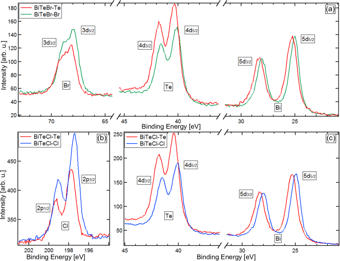
To gain further insight into the structural and chemical properties of the BiTeBr and BiTeCl(0001) surfaces we have performed XPS experiments. Fig. 2(a)-(c) shows core-level spectra directly corresponding to the different surfaces presented in Fig. 1. Comparing spectra for Te- and Br(Cl)-terminated surfaces we observe a relative shift of 200 meV (300 meV), which we attribute to band bending Crepaldi_PRL ; Landolt_NJP ; Moreschini . The energy shifts are slightly reduced compared to values reported in Ref. Moreschini which might be due to the higher excitation energy and thus an increased probing depth in the present experiments.
| elem.[eV] | Bi2Te3[eV] | Cl[eV] | TeCl[eV] | Br[eV] | TeBr[eV] | BiTeI[eV] | |
|---|---|---|---|---|---|---|---|
| Bi 5d5/2 | 24.1 | 24.6 | 25.0 | 25.3 | 25.0 | 25.2 | 25.0 |
| Te 4d5/2 | 40.5 | 39.9 | 40.1 | 40.4 | 40.1 | 40.3 | 40.1 |
| work function | 5.1 | 6.2 | 4.5 | 6.0 | 4.7 | (5.2) |
| BiTeCl | BiTeBr | BiTeI | |
|---|---|---|---|
| Bi | -1.09 | -1.01 | -0.91 |
| Te | +0.41 | +0.42 | +0.44 |
| +0.68 | +0.59 | +0.47 |
Considering the peak intensities for the Te and Br(Cl) species we observe characteristic differences between two surfaces with different termination resulting from the finite electron mean free path of the XPS experiment of around 1 nm Huefner . When going from Te- to -terminated surfaces the Te signal is reduced while the signal is enhanced, directly reflecting the changed atomic stacking sequence. The spectra have been normalized to the signal of Bi which for both terminations is expected to reside in the second atomic layer as shown in the inset of Fig. 1(a). For a quantitative estimation we assume an exponential damping of the signal which amounts to roughly 30% for two atomic layers and the present experimental conditions Huefner . From the data in Fig. 2(a) we infer that the Te 4d and Br 3d signals change by 22% and 25%, respectively. In Fig. 2(b)-(c) the change for the Te 4d core level is 30% and 36% for Cl 2p. Averaged over four samples, the damping for BiTeBr is 265% for Te- and 196% for Br-terminations while for BiTeCl we find 323% for Te- and 2413% for Cl-terminated surfaces. The XPS data thus confirm the single termination and the expected termination-dependent atomic layer stacking for BiTeBr and BiTeCl.
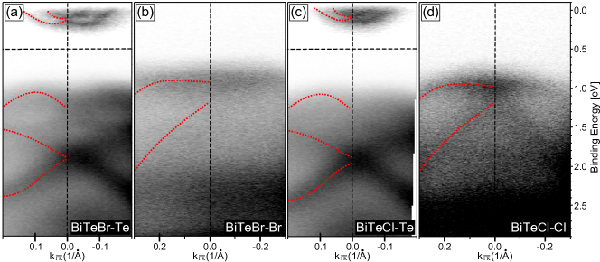
Table 1 summarizes the binding energies for the Te 4d5/2 and Bi 5d5/2 peaks in BiTe, which contain information about the chemical bonding in the compounds Huefner . The aforementioned band bending gives rise to small deviations between different terminations on the order of 200-300 meV. Furthermore, when compared to the values in Bi and Te metal Shalvoy , the Bi 5d5/2 peaks are shifted to higher and the Te 4d5/2 peaks to lower binding energies. The absolute shift is significantly larger for Bi than for Te. On the other hand, no clear trends along the series = Cl, Br, I are apparent. To gain a better understanding of the experimental data we have calculated by use of DFT the charge transfer in bulk BiTe as shown in Table 2. As one can see, the Bi atom loses about one electron by transferring it to Te (0.4 ) and atoms which is in line with the experimental result. Note that among the three compounds the values for Bi vary by only 10 - 20% and are basically the same for Te. This might explain the absence of clear chemical trends in the respective XPS binding energies. The considerable increase in the calculated charge transfer to along = I, Br, Cl further indicates an increasingly ionic bonding character between and BiTe+ layer with rising electronegativity of the halogen atoms.
Additional insight into the influence of the halogen species on the bonding character may be gained by a comparison to Bi2Te3, showing a similarly layered structure as BiTe, where a single Bi layer resides between two Te layers (see e.g. Ref. Kuznetsov ). For this compound the chemical shift of the Bi 5d5/2 line is considerably reduced (see Table 1). This points to significant differences between BiTe and Bi2Te3, for which the bonding is usually assumed to be dominated by covalent contributions Wagner .
Table 1 also displays work functions for BiTe as determined by the secondary photoelectron cutoff. For = Cl, Br large differences above 1 eV between - and Te-terminated surfaces are observed in quantitative agreement with a recent STM study of the local work function on BiTeI(0001) Kohsaka . This finding may indeed be understood in terms of an ionic bonding between and BiTe+ layers creating opposite dipoles near the surface depending on termination Shevelkov ; Eremeev_NJP ; Crepaldi_PRL ; Tournier ; Moreschini ; Butler ; Ishizaka . Furthermore, the larger calculated charge transfer in BiTeCl compared to BiTeBr is in line with the increased work function difference between the two terminations observed experimentally. The work function for a Bi2Te3(0001) surface, which is terminated by a Te layer Kuznetsov , is considerably larger than for the Te-terminated BiTeBr and BiTeCl surfaces, again pointing to a strong effect of the halogen atoms on the microscopic charge distribution. Surprisingly, for BiTeI only one cutoff could be observed in our spectra despite the presence of Te- and I-terminated surface areas. The Te and I domains of BiTeI are in order of 100 nm Fiedler and maybe small enough to result in a mixed work function when measured by secondary electron cutoff technique. The corresponding work function of 5.2 eV is given in brackets in Table 1 and lies in between the values found for Te- and I-terminated surface areas by STM Kohsaka .
III.2 Surface electronic structure
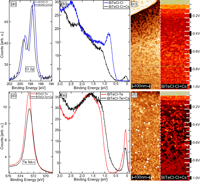
Fig. 3 shows ARPES data obtained for BiTeBr and BiTeCl(0001) surfaces. The band structures vary greatly between Te- and Br/Cl-terminated surfaces, but, for a given termination, are similar for both materials. This is in agreement with previous results Moreschini . On the Te-terminated surface we observe a Rashba-split band close to the Fermi level that derives from the conduction band bottom and the onset of valence band states at a binding energy of approximately 1 eV. We note that only one set of parabolic bands is visible in our data whereas previous studies observed two to three sets of bands Sakano_PRL ; Crepaldi_PRB . In Refs. Sakano_PRL ; Crepaldi_PRB the lowest detected bands have their minima below -0.4 eV while in our case at roughly -0.2 eV. This could point to a different n-type doping at the surface or in the bulk. Another possible explanation are strong cross section effects with excitation energy which were reported recently Crepaldi_PRB . For the Br/Cl-terminated surface conduction band states do not appear at the Fermi level due to p-type band bending as well as no surface states emerge near the valence band in agreement with earlier ARPES measurements on BiTeCl and in contradiction with a theoretical prediction Landolt_NJP . The onset of spectral weight derived from the valence band lies at binding energies of approximately 0.7 - 0.8 eV.
The electronic structure determined by ARPES is in fair agreement with the dI/dV maps in Fig. 1, concerning, e.g., the presence or absence of surface states at the Fermi level depending on termination. In accordance with previous findings for BiTeI we observe significant time-dependent shifts to higher binding energies in the electronic structure of the -terminated surfaces while those are much reduced for the Te-termination Fiedler . This can be attributed to residual gas absorption that is enhanced for the -terminations, as already suggested by our STM data. More rapid energy shifts were observed during operation of the He lamp, possibly as a result of hydrogen adsorption, which might explain the discrepancy between the valence band offsets determined by ARPES (Fig. 3) and by the dI/dV maps in Fig. 1 as well as the absence of the surface states on the terminations.
Similar to the XPS spectra in Fig. 2 also the ARPES data in Fig. 3 reflect the complete surface area of our samples because the spot sizes of the light sources exceed the lateral sample dimensions. The results therefore confirm the single termination of BiTeBr and BiTeCl on a macroscopic scale, in line with the STM data in Fig. 1. This excludes any considerable appearance of different crystal phases. The measured band structures show no topological surface state that would bridge the gap between valence and conduction bands, excluding a possible topological insulator phase in BiTeCl Chen ; Yan .
Since the electronic structure of BiTe near the surface is highly termination-dependent it is of interest to investigate additional possibilities to modify the surface electronic properties. Fig. 4 summarizes the influence of Cs adsorption on the surfaces of BiTeCl. Surprisingly, we observe energy shifts in the spectra into opposite directions for the two terminations: While for the Cl-terminated surface the features shift to higher binding energy - as expected for adsorption of alkali species Crepaldi_PRL ; Fiedler ; Seibel - they shift to lower binding energy for the Te-terminated surface. This trend is observed in the valence band [see Fig. 4(b),(e)] and in the core levels [see Fig. 4(a),(d)]. The positive energy shift on the Te-terminated surface is rather unusual and may occur in the present case due to clustering of the Cs adsorbates, as observed by STM in Fig. 4(f). In Ref. Fiedler we showed for BiTeI that the diffusion length of Cs atoms at room-temperature is considerably higher for Te- than for I-terminated surfaces Fiedler , which could explain the strong clustering observed in Fig. 4(f). For the Cl-termination the appearance of the Cs-induced structures in STM is different and reveals flatter areas with reduced dI/dV signal (see Fig. 4(c)). As seen in Fig. 4(b) the conduction band minimum shows up below the Fermi level upon Cs deposition on the Cl-terminated surface, indicating that it is located slightly above the Fermi level for the pristine surface. In summary, the results indicate that the surface termination can considerably affect the adsorption behavior of adatoms and the resulting influence on the electronic structure, which might be of relevance, e.g., for interfacing BiTeX with other materials. Similar effects as presented here for Cs/BiTeCl were also observed for Cs/BiTeBr (not shown), namely an energy shift to higher binding energies on the Br-termination and a clustering of Cs on the Te-termination in combination with an energy shift to lower binding energies.
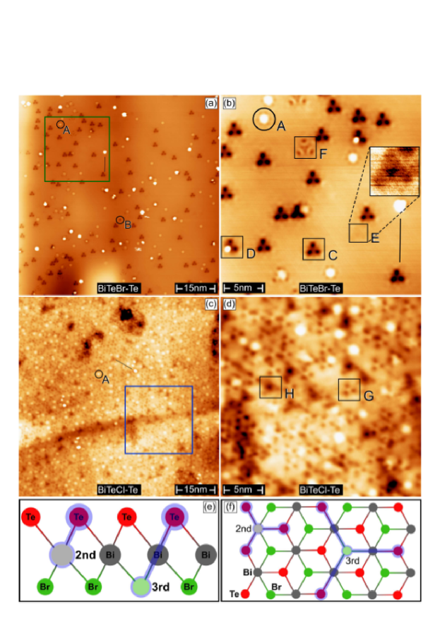
III.3 Atomic defects
After identifying the surface termination, we re-glued the samples with a top-post and moved them to a separate LT-STM, operated at = 5 K, to cleave them again. Fig. 5 shows data obtained at a positive gap voltage, usually resulting in increased (decreased) contrast for defects that act as electron donors (acceptors) Jiang .
If we assume that the sample only consists out of three elements, for example Bi, Te and Br, three kinds of defects may appear, e.g. in the Br layer: a vacancy, a Te antisite and a Bi antisite. We expect that the electronegativity behaves as Bi < Te < Br (as shown in our DFT calculations) and that charge of two neighboring atoms is transferred from the one with lower to the one with higher electronegativity. The atomic radii behave as Bi > Te > Br. One can assume that it is more likely for a vacancy to be substituted by a smaller atom than forming an antisite with a larger atom.
In another publication we showed a 400 nm2 scan of the Te termination of BiTeI Fiedler which revealed defect densities of roughly 7.5/(100 nm2) in the third layer (I) and 2.5/(100 nm2) in the first layer (Te). Fig. 5(a) shows the Te termination of BiTeBr (scan area 75 nm75 nm) measured at 1 V gap voltage and 10 pa tunneling current. With the same method Jiang , we can identify defect densities of about 2.5/(100 nm2) in the third layer (Br) and 1.3/(100 nm2) in the first layer (Te). No defects in the second layer (Bi) have been found.
Adsorbates, marked by a black arrow, appear to be around 2.5 nm high and vary in shape, while defects labeled (A) are only 25 pm high and 1 nm in diameter. They show an increased contrast and in the zoom-in in Fig. 5(b) one further recognizes that the atoms around the defect center appear darker. This is an indication for a local charge transfer from the surrounding to the defect atom. Defect (B) shows a reduced DOS indicating a charge transfer from the defect to the surrounding. Comparing the defects (A) and (B) by means of total numbers and relative contrast, we conclude that (A) is a Br antisite while (B) is most likely a Bi antisite or a vacancy.
Now we analyze the three different third layer defects by means of total number and relative contrast. Defect (C) appears most often and features the highest contrast. Since the third layer of the Te termination of BiTeBr is Br, having the smallest atomic radius and largest electronegativity, a Br vacancy could be a reasonable candidate. Furthermore, the basic structure of defect (D) is the same defect as (C) with an additional atom on top. A possible explanation is a Br atom which remains on the surface after the cleaving process. Defect (E) appears less often than (C) but more often than defect (F) and has the lowest contrast. The atomic radius of Br is closer to Te than to Bi, which would lead to a Te antisite in the Br layer. Also the fact that the contrast is weak could be due to the smaller difference in electronegativity of Te and Br compared to Bi. (F) is the defect that appears most rarely, which may indicate a Bi antisite in the Br layer. The high contrast contradicts this assumptions, but a closer comparison between (C) and (F) shows an inversion of the contrast. While the center of defect (C) shows a higher DOS than the direct surrounding, for (F) the situation is opposite: a low intensity in the center with a bright surrounding. If we expect a Bi antisite in the Br layer, the Bi would donate an electron, which would result in a higher DOS at the location of the defect Jiang . Also the center of defect (E) shows a dark contrast with a brighter surrounding which would be in line with our assumptions, since both Bi and Te are less electronegative compared to Br, so they would act as electron donors.
Fig. 4(e) and (f) provide side- and top-view sketches of particular atomic defects in the second a third atomic layer, respectively. While a defect in a certain layer affects nearest neighbors (NN) atoms, the resulting pattern on the surface gets more extended the deeper the defect is located. A second layer defect (2nd) would result in a contrast change of three NN atoms on the surface. A third layer defect (3nd) results in a contrast change of three next-nearest neighbor surface atoms, as can be seen in Fig. 4(b) defect C. Defects like E and F appear, when the third layer defect (Br) influences the NN (Bi / 2nd layer) differently, e.g. acting as an electron donor instead of an electron acceptor. The result is a Bi atom acting like a 2nd layer defect and therefore in three Bi atoms influencing three neigboring atoms (Te) each.
Like on BiTeI Fiedler no defects below the third layer could be found, possibly due to the van-der-Waals gap. The whole surface seems to be corrugated, as can be seen on the bottom part of Fig. 5(a) at the dark and bright area, which might be the result of screw dislocations. If we compare the Te termination of BiTeBr and BiTeI, the defects E and F of Fig. 5(a) are very similar to the defects E and F from Fig. 2 in Ref. Fiedler , which could also be Te and Bi antisites.
The defect density in BiTeCl [Fig. 5(c)] is much higher as compared to BiTeBr. It is difficult to find a vacancy in the first layer but adsorbates (black arrow) and antisites (A) can frequently been found. Fig. 5(d) is the magnified view of the blue-framed square shown in Fig. 5(c). It is hard to point out certain defects but (G) and (H) probably represent different third layer defects, most likely a vacancy and a Te antisite, respectively.
So far measurements in the LT-STM were only successful for the Te-terminated surfaces of BiTeBr and BiTeCl. However, third layer defects of Te should be equal to first layer defects of , as long as they are not induced by the cleaving process. This would mean at least for BiTeBr that the Bi layer is almost free of defects and that the Te-layer has less defects than the Br layer.
IV Discussion
Comparing the three BiTe compounds the most obvious difference is the presence ( = I) or absence ( = Cl, Br) of stacking faults in the bulk crystal structure resulting in surfaces with mixed or single terminations, respectively. On the atomic scale, however, BiTeCl stands out with a considerably larger defect density than the two other compounds. Hence, in this respect BiTeBr currently appears to be the material with the most homogeneous structural properties. This finding nicely complements comparative studies of the surface electronic properties of BiTe that suggests BiTeBr as the best candidate for possible future applications Eremeev_NJP ; Moreschini .
We further note that a possible migration of Bi atoms into the topmost Te-layer was speculated to occur in all three BiTe compounds based on the observation of a second component in the Bi core level signal for Te-terminated surfaces Moreschini . In our STM measurements for BiTeBr, however, such defects involving the first (Te) and the second (Bi) layer are not found. On the other hand, also no additional component in the Bi core level spectra is observed in the present study, in agreement with a previous report on BiTeCl Landolt_NJP .
The role of structural defects is furthermore important for a basic understanding of the electronic properties in BiTe. For BiTeCl a lift-off during the cleaving process of a thin free-standing layer (around 1 unit cell) that remains loosely on the crystal surface has been proposed to give rise to the Rashba-split surface bands observed in ARPES and to mask the presence of a topological state on the intrinsic surface Chen . This scenario is not supported by the present combined STM and ARPES results that show step edge heights of the surface terraces matching the bulk unit cell and, at the same time, provide no indication of topological surface bands. It is furthermore worth noting that, while the atomic defect density observed here in STM is considerably higher for BiTeCl than for BiTeBr, the quality of the ARPES data turns out to be comparable and also the measured band structures are very similar. This observation is in contrast to a recent investigation of BiTeCl that concluded qualitative changes in the electronic structure depending on the amount of defects near the surface Yan .
The broken inversion symmetry in BiTe in combination with the high electronegativity of the halogen atoms is assumed to induce a net dipole moment in the bulk unit cell Chen ; Kohsaka that, in turn, gives rise to n- or p-type band bending at the surface depending on termination Crepaldi_PRL . The proposed microscopic picture of the charge distribution is often based on a covalently bound (BiTe)+ bilayer that couples ionically to the adjacent layer Shevelkov ; Crepaldi_PRL ; Moreschini ; Butler . However, the bonding character has also been viewed as ionic for, both, Bi-Te and Bi- based on the fact that the valence (conduction) band is to most extent Te/ (Bi) derived which indicates significant charge transfer from Bi to Te and Zhu . In some calculations even a larger charge transfer to Te than to has been obtained Chen ; Ma . Direct experimental information on this issue has so far been scarce. The present XPS measurements indeed point to a substantial charge donation from Bi to Te and which is in line with our first-principles calculations of the local atomic charges. On the other hand, the large work function differences between Te- and -terminated surfaces confirm the presence of a dipole moment in the unit cell and, thus, support the view of a (BiTe)+ block with positive net charge that forms a polar bond with the layer.
V Summary
We have presented a comparative study of the structural and electronic surface properties of the non-centrosymmetric giant-Rashba semiconductors BiTe(0001) ( = Cl, Br, I). Cleaving of single-crystalline samples exposes macroscopically homogeneous surfaces with Te- and -termination for BiTeCl and BiTeBr, in contrast to BiTeI where bulk stacking faults are known to give rise to mixed surface terminations. STM and XPS data confirm the unit cell heights and atomic stacking orders that are expected from the bulk crystal structure. The electronic band structures measured by ARPES differ considerably depending on surface termination, but in no case topological surface states are observed. The chemical bonding in BiTe is found to be characterized by substantial charge transfer from Bi to Te and . However, based on work function measurements we also obtain evidence for ionic bonding between (BiTe)+ bilayers and layers, whereas the polarity of the bond increases with rising electronegativity of the halogen atom.
VI Acknowledgements
This work was financially supported by the Deutsche Forschungsgemeinschaft through FOR1162 and partly by the Ministry of Education and Science of Russian Federation (Grant No. 2.8575.2013), the Russian Foundation for Basic Research (Grants No. 15-02-01797, 15-02-02717) and Saint Petersburg State University (project 11.50.202.2015).
References
- (1) K. Ishizaka, M. S. Bahramy, H. Murakawa, M. Sakano, T. Shimojima, T. Sonobe, K. Koizumi, S. Shin, H. Miyahara, A. Kimura, K. Miyamoto, T. Okuda, H. Namatame, M. Taniguchi, R. Arita, N. Nagaosa, K. Kobayashi, Y. Murakami, R. Kumai, Y. Kaneko, Y. Onose and Y. Tokura, Nature Mater. 10, 521 (2011).
- (2) S. V. Eremeev, I. A. Nechaev, Yu. M. Koroteev, P. M. Echenique, and E. V. Chulkov, Phys. Rev. Lett. 108, 246802 (2012).
- (3) H. Murakawa, M. S. Bahramy, M. Tokunaga, Y. Kohama, C. Bell, Y. Kaneko, N. Nagaosa, H. Y. Hwang and Y. Tokura, Science 342, 6165 (2013).
- (4) A. Crepaldi, L. Moreschini, G. Autès, C. Tournier-Colletta, S. Moser, N. Virk, H. Berger, Ph. Bugnon, Y. J. Chang, K. Kern, A. Bostwick, E. Rotenberg, O. V. Yazyev, and M. Grioni, Phys. Rev. Lett. 109, 096803 (2012).
- (5) G. Landolt, S. V. Eremeev, Y. M. Koroteev, B. Slomski, S. Muff, T. Neupert, M. Kobayashi, V. N. Strocov, T. Schmitt, Z. S. Aliev, M. B. Babanly, I. R. Amiraslanov, E. V. Chulkov, J. Osterwalder and J. H. Dil, Phys. Rev. Lett. 109, 116403 (2012).
- (6) G. Landolt, S. V. Eremeev, O. E. Tereshchenko, S. Muff, B. Slomski, K. A. Kokh, M. Kobayashi, T. Schmitt, V. N. Strocov, J. Osterwalder, E. V. Chulkov and J. H. Dil, New J. Phys. 15, 085022 (2013).
- (7) M. Sakano, M. S. Bahramy, A. Katayama, T. Shimojima, H. Murakawa, Y. Kaneko, W. Malaeb, S. Shin, K. Ono, H. Kumigashira, R. Arita, N. Nagaosa, H. Y. Hwang, Y. Tokura, and K. Ishizaka, Phys. Rev. Lett. 110, 107204 (2013).
- (8) L. Moreschini, G. Autès, A. Crepaldi, S. Moser, J.C. Johannsen, K.S. Kim, H. Berger, Ph. Bugnon, A. Magrez, J. Denlinger, E. Rotenberg, A. Bostwick, O.V. Yazyev and M. Grioni, J. Electron Spectroscopy and Related Phenomena 201, 115–120 (2015).
- (9) C. Martin, E.D. Mun, H. Berger, V. S. Zapf and D. B. Tanner, Phys. Rev. B bf 87, 041104(R) (2013).
- (10) C. Bell, M. S. Bahramy, H. Murakawa, J. G. Checkelsky, R. Arita, Y. Kaneko, Y. Onose, M. Tokunaga, Y. Kohama, N. Nagaosa, Y. Tokura and H. Y. Hwang, Phys. Rev. B bf 87, 081109(R) (2013).
- (11) M. S. Bahramy, R. Arita and N. Nagaosa, Phys. Rev. B bf 84, 041202(R) (2011).
- (12) M.S. Bahramy, B.-J. Yang, R. Arita and N. Nagaosa Nature Commun. 3, 679 (2011).
- (13) S. Datta and B. Das, Appl. Phys. Lett. 56, 665 (1990).
- (14) I. Z̆utić , J. Fabian and S. D. Sarma, Reviews Of Modern Physics 76 (2004).
- (15) C. R. Ast, J. Henk, A. Ernst, L. Moreschini, M. C. Falub, D. Pacilé, P. Bruno, K. Kern and M. Grioni, Phys. Rev. Lett. 98, 186807 (2007).
- (16) H. Bentmann, F. Forster, G. Bihlmayer, E. V. Chulkov, L. Moreschini, M. Grioni and F. Reinert, New J. Phys. 87, 37003 (2009).
- (17) L. El-Kareh, P. Sessi, T. Bathon and M. Bode, Phys. Rev. Lett. 110, 1706803 (2013).
- (18) L. El-Kareh, G. Bihlmayer, A. Buchter, H. Bentmann, S. Blügel, F. Reinert and M. Bode, New J. Phys. 16, 045017 (2014).
- (19) S.V. Eremeev, I.P. Rusinov, I.A. Nechaev and E.V. Chulkov, New J. Phys. 15, 075015 (2013).
- (20) C. J. Butler, H.-H. Yang, J.-Y. Hong, S.-H. Hsu, R. Sankar, C.-I Lu, H.-Y. Lu, K.-H. O. Yang, H.-W. Shiu, C.-H. Chen, C.-C. Kaun, G.-J. Shu, F.-C. Chou and M.-T. Lin, Nature Commun. 5, 4066 (2013).
- (21) C. Tournier-Colletta, G. Autès, B. Kierren, Ph. Bugnon, H. Berger, Y. Fagot-Revurat, O. V. Yazyev, M. Grioni and D. Malterre, Phys. Rev. B 89, 085402 (2014).
- (22) Y. Kohsaka, M. Kanou, H. Takagi, T. Hanaguri and T. Sasagawa, Phys. Rev. B 91, 245312 (2015).
- (23) S. Fiedler, L. El-Kareh, S. V. Eremeev, O. E. Tereshchenko, C. Seibel, P. Lutz, K. A. Kokh, E. V. Chulkov, T. V. Kuznetsova, V. I. Grebennikov, H. Bentmann, M. Bode and F. Reinert, New J. Phys. 16, 075013 (2014).
- (24) Y. J. Yan, M. Q. Ren, X. Liu, Z. C. Huang, J. Jiang, Q. Fan, J. Miao, B. P. Xie, T. Zhang and D. L. Feng, arXiv arXiv:1502.07080 (2015).
- (25) A. Crepaldi, F. Cilento, M. Zacchigna, M. Zonno, J. C. Johannsen, C. Tournier-Colletta, L. Moreschini, I. Vobornik, F. Bondino, E. Magnano, H. Berger, A. Magrez, Ph. Bugnon, G. Autès, O. V. Yazyev, M. Grioni and F. Parmigiani, Phys. Rev. B. 89, 125408 (2014).
- (26) Y. L. Chen, M. Kanou, Z. K. Liu, H. J. Zhang, J. A. Sobota, D. Leuenberger, S. K. Mo, B. Zhou, S-L. Yang, P. S. Kirchmann, D. H. Lu, R. G. Moore, Z. Hussain, Z. X. Shen, X. L. Qi and T. Sasagawa, Nature Phys. 9, 704-708 (2013).
- (27) I. Horcas, R. Fernández, J. M. Gómez-Rodríguez, J. Colchero, J. Gómez-Herrero and A. M. Baro, Rev. Sci. Instrum. 78, 013705 (2007).
- (28) Sergio Trasatti, Electroanalytlcal Chemtstry and Interfactal Electrochemistry 54, 19-24 (1974).
- (29) P. C. Rusu and G. Brocks, Phys. Rev. B 74, 073414 (2006).
- (30) A. Tomokiyo, T. Okada and S. Kawano, Jpn. J. Appl. Phys. 16, 291 (1977).
- (31) U. Petasch, C. Hennig and H. Oppermann, Untersuchungen zum quasibinären System Bi2Te3/BiCl3 Z. Naturforsch. 54 b, 234-238 (1999).
- (32) K.A. Kokh, S.V. Makarenko, V. Golyashov, O.A. Shegai, O.E. Tereshchenko, CrystEngComm 16, 581 (2014)
- (33) P. E. Blöchl, Phys. Rev. B 50, 17953 (1994).
- (34) G. Kresse and D. Joubert, Phys. Rev. B 59, 1758 (1999).
- (35) J. P. Perdew, K. Burke and M. Ernzerhof, Phys. Rev. Lett. 77, 3865 (1996).
- (36) G. Kresse and J. Hafner, Phys. Rev. B 48, 13115 (1993).
- (37) G. Kresse and J. Furthmüller, Comput. Mater. Sci. 6, 15 (1996).
- (38) W. Tang, E. Sanville, and G. Henkelman, J. Phys.: Condens. Matter 21, 084204 (2009).
- (39) A. V. Shevelkov, E. V. Dikarev, R. V. Shapanchenko and B. A. Popovkin, J. Solid State Chem. 114, 379 (1995).
- (40) S. Hüfner, Photoelectron Spectroscopy - Principles and Applications. Springer Verlag 3rd ed., (2003).
- (41) R. B. Shalvoy, G. B. Fisher, and P. J. Stiles, Phys. Rev. B 15, 1680 (1977).
- (42) M. V. Kuznetsov, L. V. Yashina, J. Sánchez-Barriga, I. I. Ogorodnikov, A. S. Vorokh, A. A. Volykhov, R. J. Koch, V. S. Neudachina, M. E. Tamm, A. P. Sirotina, A. Yu. Varykhalov, G. Springholz, G. Bauer, J. D. Riley and O. Rader, Phys. Rev B 91, 085402 (2015).
- (43) V. Wagner, G. Dolling, B. M. Powell and G. Landwehr, Phys. stat. sol. (b) 85, 311 (1978).
- (44) C. Seibel, H. Maaß, M. Ohtaka, S. Fiedler, C. Jünger, C.-H. Min, H. Bentmann, K. Sakamoto and F. Reinert, Phys. Rev. B 86, 161105(R) (2012).
- (45) Y. Jiang, Y. Y. Sun, M. Chen, Y. Wang, Z. Li, C. Song, K. He, L. Wang, X. Chen, Q.-K. Xue, X. Ma and S. B. Zhang, Phys. Rev. Lett. 108, 066809 (2012).
- (46) Z. Zhu, Y. Cheng and U. Schwingenschlögl New J. Phys. 15, 023010 (2013).
- (47) Y. Ma, Y. Dai, W. Wei, X. Li and B. Huang, Phys. Chem.Chem. Phys. 16, 17603 (2014).