Spin-orbit splitting of valence and conduction bands in HgTe quantum wells near the Dirac point
Abstract
Energy spectra both of the conduction and valence bands of the HgTe quantum wells with a width close to the Dirac point were studied experimentally. Simultaneous analysis of the Shubnikov-de Haas oscillations and Hall effect over a wide range of electron and hole densities gives surprising result: the top of the valence band is strongly split by spin-orbit interaction while the splitting of the conduction band is absent, within experimental accuracy. Astonishingly, but such a ratio of the splitting values is observed as for structures with normal spectrum so for structures with inverted one. These results do not consistent with the results of kP calculations, in which the smooth electric filed across the quantum well is only reckoned in. It is shown that taking into account the asymmetry of the quantum well interfaces within a tight-binding method gives reasonable agreement with the experimental data.
pacs:
73.20.Fz, 73.21.Fg, 73.63.HsI Introduction
Heightened interest to two-dimensional (2D) structures with quantum well of gapless semiconductors is caused by the fact that different types of the carrier energy spectrum could be realized in these structures depending on the width () of quantum well. The most detailed, both theoretically and experimentally, heterostructures with Hg1-xCdxTe/HgTe/Hg1-xCdxTe quantum well were studied. The calculations of the energy spectrum in framework of kP method for symmetrical quantum well show that there is the critical width of the HgTe quantum well, nm, when the linear in quasimomentum Dirac-like energy spectrum should be realized at small quasimomentum () [1, 2]. At the energy spectrum is normal. The valence band is formed from heavy-hole states while the conduction band is formed from electron states and states of light hole. At these states swap over, and such a spectrum is called an inverted spectrum. Another approach, the calculation in the framework of tight-binding model, which takes into account the bulk inversion asymmetry of the zinc blende lattice, gives close result regarding the dependence except the fact that the relatively large anti-crossing at and large spin-orbit (SO) splitting of the conduction and valence band appears at .
Knowledge of the energy spectrum is necessary for an understanding of all properties of 2D systems: optical, transport and others. However it has been experimentally studied rather superficially to date. The energy spectrum of the conduction band was studied more detailed [3, 4, 5, 6, 7]. There was shown that the SO splitting of the conduction band in the technologically symmetric quantum wells was not reveal itself in the most cases, the effective mass of the electrons increased with their density. These data were found in satisfactory agreement with results of theoretical calculations performed in the framework of the kP method.
The energy spectrum of the valence band is investigated still less and, what is important, the experimental data are inconsistent with theoretical results in many cases. So in the structures with nm that corresponds to the inverted energy spectrum, the hole effective mass () within wide hole density range cm-2 occurs substantially less than that calculated within kP method: [8, 9, 10] instead of [11]. These calculations predict also that the conduction band should overlap with the valence band which top is located at when nm. Although this prediction is in qualitative agreement with experimental data [12, 10], the quantitative difference between theory and experiment is drastic. Experimentally, the top of the valence band is located at cm-1, while the theoretical prediction gives the value of about cm-1.
The valence band spectrum in the heterostructures with normal band ordering was studied in several papers only. The experimental data published in Refs. [13] and [14] for structures with nm are very similar however the interpretation differs significantly. Analyzing the Hall density and the Fourier spectra of the Shubnikov-de Haas (SdH) oscillations, the authors of Ref. [13] are able to describe the data taking into account the secondary maxima of the dispersion law located at . But it has been done only for one hole density. Studying analogous heterostructures, the authors of Ref. [14] show that such interpretation does not describe the experimental data within a wide hole density range. They show that all the results are well described under assumption that the top of the valence band is very strongly split by SO interaction. They supposed that the reason for such a splitting is a strong electric field of p-n junction of technological origin in which the quantum is embedded. The authors were unable to investigate the splitting of the conduction band. These data would make the interpretation more reliable.
In the present paper, we report the results of an experimental study both of hole and electron transport in HgTe quantum well of different width near the critical point with a normal and inverted energy spectra. The measurements were performed over a wide range of carrier density. It has been experimentally found that the valence band is strongly split by SO interaction, while the conduction band remains unsplit independently of energy band ordering. We believe that the natural interface inversion asymmetry of zinc-blende heterostructures is responsible for these peculiarities. Quantitatively, the experimental data are well described in the framework of atomistic calculation [15].
II Experimental
Our samples with HgTe quantum wells were realized on the basis of HgTe/Hg1-xCdxTe () heterostructures grown by molecular beam epitaxy on GaAs substrate with the (013) surface orientation [16]. The samples were mesa etched into standard Hall bars of mm width and the distance between the potential probes of mm. To change and control the carrier density in the quantum well, the field-effect transistors were fabricated with parylene as an insulator and aluminium as a gate electrode. For each heterostructure, several samples were fabricated and studied. The measurements were performed at temperatures of K.
III Characterization of samples regarding the type of spectrum
It is very important for interpretation of the experimental results to know whether the spectrum of structure under study is normal or inverted. The values of quantum well width presented in the Table 1 are technological, therefore it is very desirable to have independent data on the spectrum type.
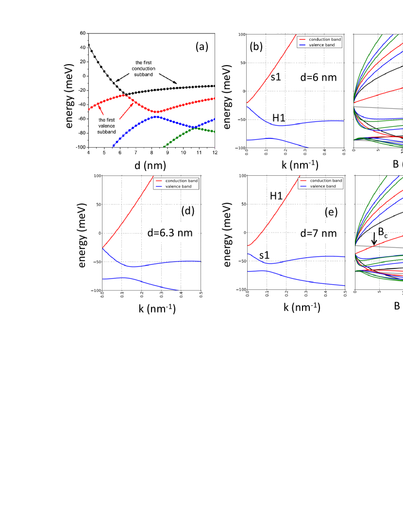
The most reliable method to determine the type of the spectra can be based on the peculiarity of the spectrum quantization in the external magnetic field. Theoretical calculations [5, 17, 11] and experimental investigations [17, 10] show that there are two anomalous Landau levels which behavior is radically different for the normal and inverted spectra [Figs. 1(c) and 1(f)].
As seen from Fig. 1(f) the Landau levels and in the structure with inverted spectrum start at from the bottom of the conduction band and top of the valence, respectively, and moving towards each other cross in the magnetic field . This magnetic field increases with increase, achieves maximal value of about T at nm and then decreases with a further increase. In the structures with normal spectrum, the energy positions of the anomalous Landau levels at is opposite: the level starts from the valence band top while the level goes from the conduction band bottom. Because they move in the same directions as for , the crossing does not occur in this case [Fig. 1(c)]. Thus, if the crossing of Landau levels is detected experimentally, the real width of the HgTe quantum well is greater than critical value and the sample under study is in inverted regime.
When is large enough so that the anomalous Landau levels have a large density of states and are well separated, the cross manifests itself as the nonmonotonic peculiarity in the vs and vs dependences [10]. When the quantum well width is close to the critical value , the cross of the Landau levels occurs at so low magnetic field that it may not reveal itself in magnetotransport measurements. It is possible in this case to observe the cross by studying the behavior of the quantum capacitance () in the magnetic field at the gate voltages close to the charge neutrality point (CNP). Unlike the resistance components which depend not only on the density of states () but on the disorder strength also, the quantum capacitance depends on the density of states only, , where stands for the chemical potential. So, the value of at should increase with growing , achieve the maximal value at and, then, decrease with the further increase of magnetic field even when the Landau levels are rather broadened. When the Fermi level is located in the bands at , the maximum in the dependence should be also observed but in the higher magnetic fields as compared with .
In the structures with normal energy spectrum, the anomalous Landau levels are moving apart and the density of states in the gap (which is nonzero due to smearing) decreases with growing magnetic field. Thus, the capacitance should decrease with near CNP.
| # | (nm) | (cm-2) | (T) | (cm-2)111At . | |
|---|---|---|---|---|---|
| 1122 | 5.6 | ||||
| H724 | 5.8 | ||||
| 1123 | 6.0 | ||||
| 1121 | 6.3 | ||||
| 1023 | 6.5 | ||||
| 222After illumination. | |||||
| 1022 | 6.7 | ||||
| 222After illumination. | |||||
| 1124 | 7.1 |
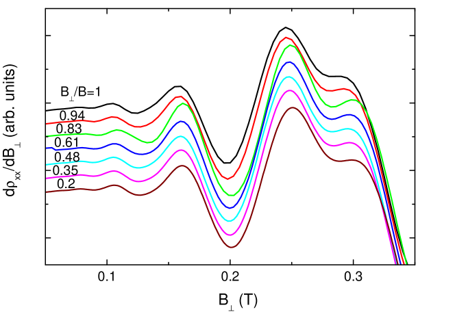
The measurements of the quantum capacitance were taken in all the structures investigated. In Fig. 2 we have presented, as an example, the dependence measured at on the structure 1023. The nonmonotonic volt-capacitance characteristic is consequence of the nonmonotonic energy dependence of the density of states. The minimum in the vicinity of CNP is observed when the Fermi level goes through the energy gap where the density of states is much smaller than that in the valence and conduction bands 222The details of capacitance measurements for HgTe quantum wells of the different widths are beyond the scope of this paper and will be published elsewhere.. The upper inset in Fig. 2 shows the magnetic field dependences of at different near CNP. The maximum in these curves at , which shifts to the higher values when deviates from CNP, is clearly evident. As seen from the lower inset in Fig. 2 the vs plot has a minimum and just the minimal value of T corresponds to the magnetic field in which the anomalous Landau levels and cross each other. The analogous maximum in the dependence at close to was also observed in the structures 1022 and 1121. The values obtained in such a manner for these three structures are listed in the Table 1.
As for the remaining four heterostructures, the quantum capacitance for the structure 1124 in the vicinity of CNP is practically independent on , while for the structures 1122, H724, and 1123 decreases when increases.
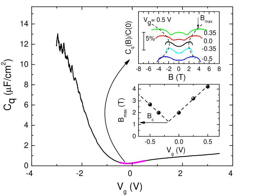
Thus the results of capacitance measurements in the presence of magnetic field show unambiguously that the structures 1022, 1023 and 1121 has inverted spectrum, the structure 1124 is very close to the critical point , while the other structures have normal spectra.
IV The valence band spectrum
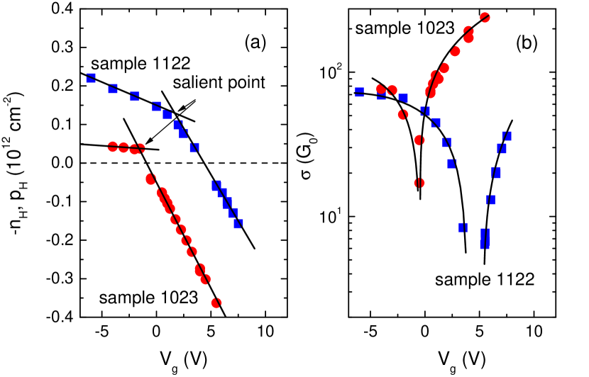
Let us now inspect the gate voltage dependences of the Hall carrier density obtained at low magnetic field [where is constant] as follows: when for electron density and when for hole density. These dependences are plotted in Fig. 3(a) for structures 1122 and 1023 with normal and inverted spectrum, respectively. The corresponding dependences of the conductivity are shown in Fig. 3(b). These structures are chosen as typical ones, the results for other structures are analogous. In what follows we will demonstrate all the results namely for these structures excepting the cases when the simultaneous analysis of results for all structures is useful. One can see that the electron density depends linearly on over the whole gate voltage range. Note that the slope coincides with the value (where is the capacitance between the 2D gas and gate electrode and is the gate area), to within experimental error. The hole density changes with the same slope, , within a restricted range only. At the gate voltage , where the hole density achieves some value , a salient point is observed. Analogous dependence was observed earlier in Refs. [19, 20]. As seen the values are significantly different for these structures: cm-2 for structure 1122 and cm-2 for structure 1023. The decrease of below can result from appearance of large enough density of states at the Fermi level, which pins it. They can be the states in the secondary maxima of the valence band spectrum at [see Fig. 1, panels (b), (d), and (e)] or some states in the barriers or at the interfaces between the layers forming the quantum well.
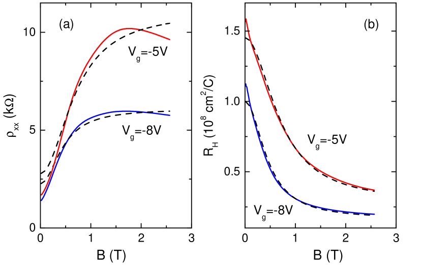
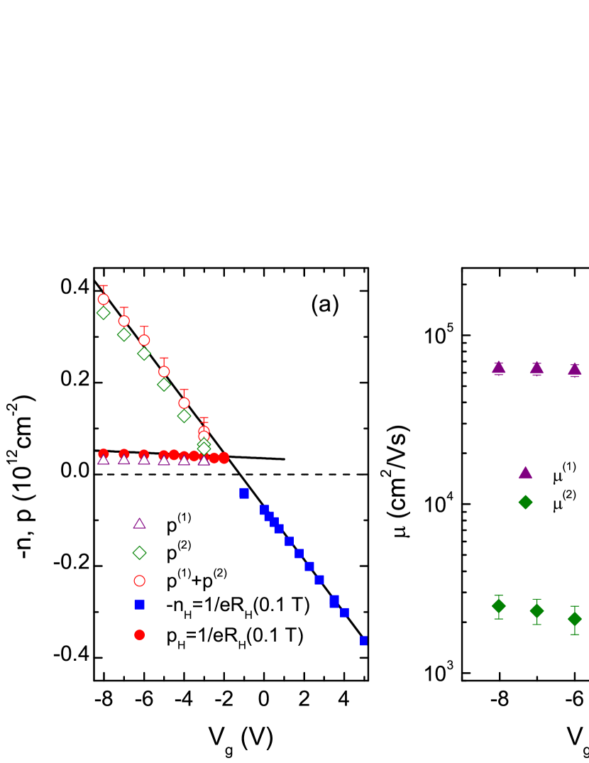
To understand which of these reasons is the primary one we analyze the magnetic field dependences of and in classically strong magnetic fields at relatively high temperature at which the SdH oscillations are suppressed. As an example, in Fig. 4 we have presented the vs and vs plots measured on the structure 1023 at K for two gate voltages. These dependences are typical for two-type carries conductivity. The simultaneous fitting of these plots by the standard hand-book expression [21] with the use of hole densities and , and hole mobilities and as the fitting parameter gives reasonable agreement with the data (see Fig. 4). The hole densities and found by this way and the total density together with the hole Hall density for different values are plotted in Fig. 5(a). It is seen that is close to and the points fall on the straight line which describes the vs data. The values of the mobility of the second type holes are about cm2/V s [see Fig. 5(b)], which beyond doubt correspond to a free carrier conductivity.
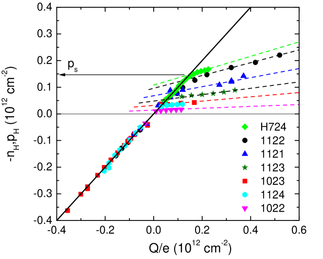
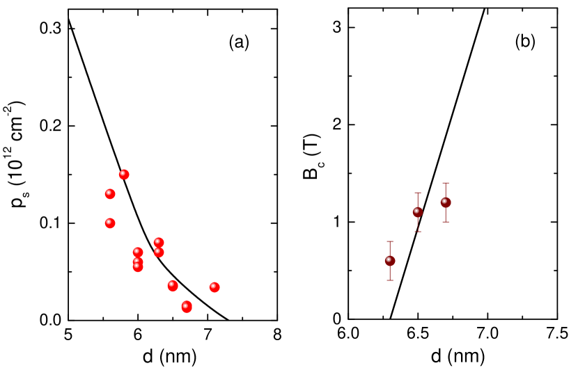
Thus, one can argue that the decrease of at is result of occupation of the secondary maxima of the valence band when the Fermi level approaches these maxima with the decreasing gate voltage. For this case the value of should monotonically depend on the quantum well width. To compare the data obtained for the different structures with different carrier density at , different insulator thickness and, hence, the different value we have plotted the values of the Hall carrier densities against the charge in the quantum well for all the structures investigated in Fig. 6. The values found from Fig. 6 are plotted against the nominal quantum well width in Fig. 7(a). The corresponding theoretical dependence calculated within framework of the Kane model in Ref. [11] is presented also. Taking into account the uncertainty in the real quantum well width and error in determination it can be concluded that the value of in such a type of heterostructures can be used to estimate the quantum well width. Note, the experimental values of are also in a satisfactory agreement with calculation results as evident from Fig. 7(b).
Before closing this section let us discuss the specific feature in the behavior of the hole density evident at . As seen from Fig. 6, the higher is the value, the larger is the slope of the dependence at . Since the Hall coefficient gives the density of holes only in the central maximum, the slope of the dependence at is determined by the relation between the densities of hole states in the central and secondary maxima and , respectively: . Thus, the increase of with growing is in qualitative agreement with the fact that the density of states in the central maximum at the energy of secondary maximum increases with the energy increase due to the nonparabolicity of dispersion law .
V Spin-orbit splitting of valence and conduction bands
Now let us turn to a more detailed study of the band spectra. To do this we have measured the SdH oscillations and their angle dependence over the wide carrier density range.
V.1 Normal band ordering
V.1.1 Valence band
Qualitatively the results obtained for structures 1122 and their interpretation are analogous to those published in Ref. [14]. Nonetheless, we briefly describe the key results that are important for the interpretation of results both for valence and conduction bands for structures with normal and inverted spectra. The gate voltage dependence of the Hall density, the dependences and taken for the structure 1122 at cm-2, and the corresponding Fourier spectrum of the SdH oscillations are presented in Fig. 8.
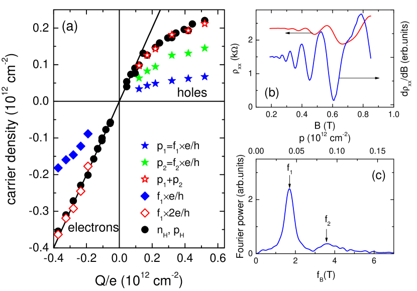
As seen from Fig. 8(c), two maxima with the frequencies and are easily detected in the Fourier spectrum. Noteworthy is that the ratio of the frequencies is close to , i.e., the Fourier spectrum is similar to the case when the spin splitting of the Landau levels manifests itself with the magnetic field increase. In such a situation the carrier density should be determined as . So, we obtain cm-2 for this concrete case. However, the Hall density at this value is significantly larger, cm-2 as seen from Fig. 8(a).
Such a difference between the hole density found from the SdH oscillations within the proposed model and the hole density found from the Hall effect takes place over the whole hole density range in all the structures investigated. Thus the interpretation described above does not correspond to our case.
The only interpretation that adequately describes our results is as follows. Each peak in the Fourier spectrum corresponds to the subband H1 which is strongly split by SO interaction into two subbands H1+ and H1-. In this case the “spin” degeneracy is lifted, and, hence, the hole densities should be found as , where indexes and correspond to H1+ and H1- subbands. So, the total hole density is . The results of such a data interpretation are presented in Fig. 8(a) within whole hole density range by stars. One can see that coincides with within experimental error. Thus, we conclude that the valence band is strongly split by SO interaction so that the ratio of hole densities in the split subbands is about over the whole hole density range.
V.1.2 Conduction band
To obtain the information on the energy spectrum and splitting of the conduction band we have thoroughly studied the electron SdH oscillations 333Due to large noisiness at positive gate voltage we could not do this in the previous our paper [14]. The possible reason of the noise can be large resistance of the p-n junctions which are formed in the 2D gas under the gate electrode edge because these structures are of p type at .. In Fig. 9(a) we have presented the SdH oscillations for some Hall densities and in Fig. 9(b), as example, the Fourier spectrum for one of them. As seen from Fig. 9(b) the Fourier spectrum consists of two peaks which characteristic frequencies differ by a factor of two analogously to the case of the hole conductivity [see Fig. 8(c)]. The main contribution to the peak with the frequency comes from the low-field SdH oscillations. Therewith, unlike the oscillations in the hole domain, the electron density found as is very close to the Hall density as evident from Fig. 8(a) indicating that the Zeeman splitting is not resolved. The peak comes from the oscillations in the high-magnetic fields and it originates from the spin split Landau levels. This corresponds to the case when the SO splitting of the conduction band is small enough.
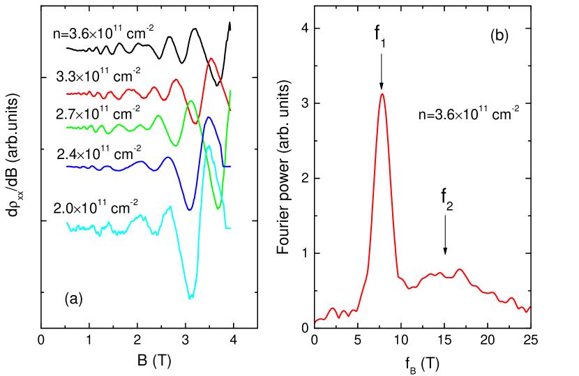
Thus, the analysis of SdH oscillations carried out over the whole carrier density range gives surprising result: the valence band is strongly split by SO interaction, while the splitting of the conduction band in the same structure does not reveal itself.
V.1.3 The Shubnikov-de Haas effect in tilted magnetic field
To ensure that our interpretation is correct one can explore the SdH oscillations in tilted magnetic field. Really, when the SO splitting is significantly smaller than the Zeeman energy (), the energy of orbital quantization depends on the normal component of the magnetic field , where is the angle between the magnetic field direction and the normal to the 2D gas plane, while the energy of spin splitting depends on total . At the low magnetic field, where the SdH oscillations are unsplit, this should manifest itself as strong angle dependence of the oscillation amplitude. In opposite case of strong spin-orbit interaction (), the spin is rigidly coupled with the orbital motion and the SdH oscillations should be determined by the normal component of the magnetic field only.
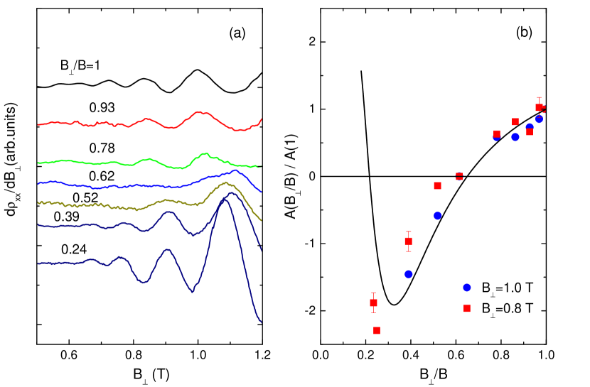
The oscillations of at T for electron density cm-2 for several tilt angles are presented in Fig. 10(a). The oscillations within this magnetic field range are caused by unsplit Landau levels. It is clearly seen that the oscillations decrease in the amplitude when deviates from the normal orientation, practically disappear at , then change the phase and increase in the amplitude at further decrease of the to ratio. This behavior results from the change of the ratio between the spin and cyclotron energies with tilt angle. Supposing and are proportional to the total magnetic field and normal component of , respectively, one can obtain the following expression for the angle dependence of the oscillation amplitude
| (1) |
This dependence together with experimental data is shown in Fig. 10(b). One can see that a good agreement is observed when .
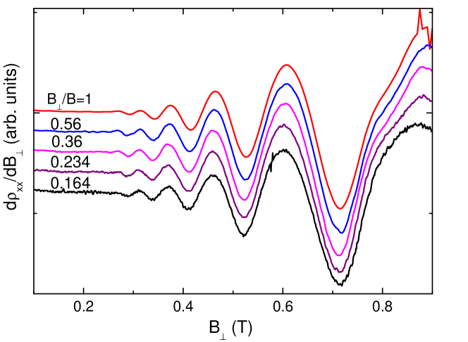
Let us now inspect the behaviour of the SdH oscillations with the changing tilt angle measured on the same heterostructure in the hole domain (Fig. 11). One can see that unlike the case of the electron conductivity, the SdH oscillations plotted against the normal component of the magnetic field remain practically unchanged with the changing tilt angle. This means that they are determined by the normal components of magnetic field only. As discussed above such a behavior should be observed when SO interaction is relatively strong: the SO splitting is much greater than the Zeeman energy. Or, alternatively, the independence of the oscillation picture on the tilt angle may caused as well by a strong anisotropy of the effective g-factor, when the in-plane g-factor is much smaller than the perpendicular one, . However, the estimation made with the use of Eq. (35) from Ref. [23] shows that it is not the case, the Zeeman splitting differs in the perpendicular and longitudinal orientations of the magnetic field only slightly for the actual quantum well widths and actual Fermi energies.
Thus, the analysis of the angle dependences of SdH oscillations also shows that the valence band spectrum is strongly split due to spin-orbit interaction, while the conduction band remains unsplit.
V.2 Inverted band ordering
The dependence of carrier densities found from the Hall and Shubnikov-de Haas effects on the charge of 2D gas for structure 1023 with inverted spectrum, nm, is plotted in Fig. 12(a). In general, it is similar to that for structure with normal spectrum excepting the fact that the value is significantly less in structures with : namely cm-2 for structure 1023 instead of cm-2 for structure 1122 with normal spectrum. As discussed in Section IV this results from the lesser energy distance between the top of the valence band at and the secondary maxima at .
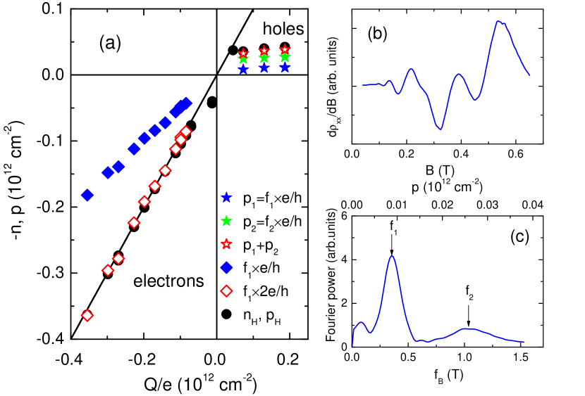
The SdH oscillations in the hole conductivity regime and their Fourier spectrum are shown in Fig. 12(b) and Fig. 12(c), respectively. As in the structures with normal spectrum, the only way, which allows us to reconcile the Hall density and data obtained from the SdH oscillations is to assume that each maximum in the Fourier spectrum is associated with the split subband.
In the electron conductivity regime, the SdH oscillations measured at different tilt angles are presented in Fig. 13(a) for the Hall density cm-2. The Fourier spectrum of the oscillations at normal orientation is shown in the inset of Fig. 13(a).
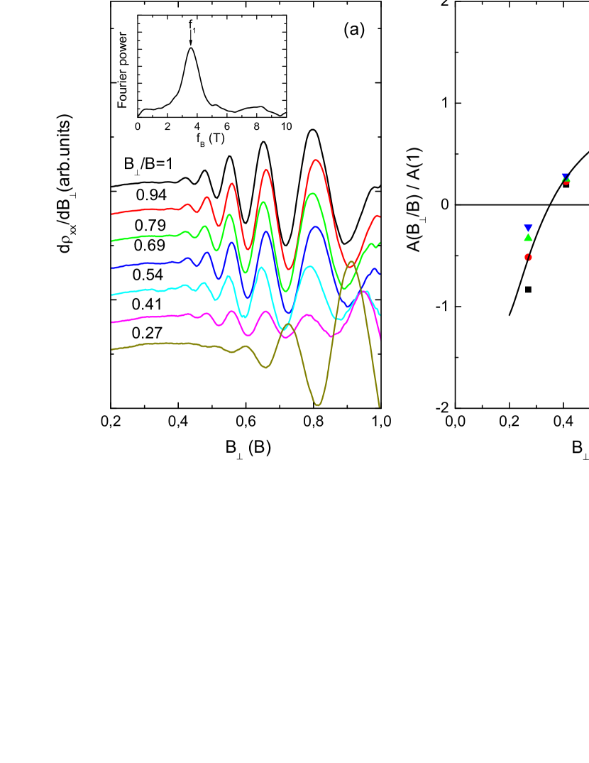
The charge dependences of the electron densities found as and are shown in Fig. 12(a). It is seen that coincides with . It means that each peak of the SdH oscillations corresponds to two fold degenerated Landau level. As Fig. 12(a) shows, such a coincidence is observed over the whole range of the electron density. Thus, the spin-orbit splitting of the conduction band in the structures with the inverted spectrum does not reveal itself as well as in the structures with normal spectrum.
The conclusion about strong splitting of the valence band and weak splitting of the conduction band is consistent with the behavior of the oscillations in tilted magnetic field.
The behavior of the oscillations of the electron conductivity with the tilt angle shown in Fig. 13(a) is analogous to that presented in Fig. 10(a) for structure with normal spectrum. The angle dependence of the oscillation amplitude in Fig. 13(b) demonstrates that the Zeeman splitting becomes equal to half orbital one at close to . The dependence calculated from Eq. (1) with well describes the data 444The detail analysis of electron-density dependence of g-factor in the structures with different width of quantum well are beyond the scope of this study and will be discuss in another paper..
The SdH oscillations of the hole conductivity measured at different tilt angle are presented in Fig. 14. As well as for the structures with normal spectrum (see Fig. 11), neither positions nor amplitudes depend on the tilt angle that corresponds to strong SO splitting of the valence band (see discussion above).
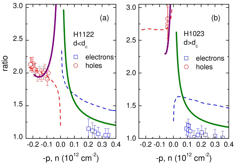
Summing up all the data given above we can formulate the main outcome. The analysis of the Shubnikov-de Haas and Hall effects over the whole carrier density range in the structures with and gives surprising result: the valence band is strongly split by SO interaction in the structures both with normal and inverted spectrum, while the splitting of the conduction band in the same structures does not reveal itself. To illustrate the written we have plotted the ratio between the carrier densities in the split subbands in the valence and conduction bands as a function of carrier density in Fig. 15 555We have plotted the ratio but not the value of SO splitting, , because to calculate from one needs the carriers effective mass which is known with some error. This figure is the key result of the paper.
VI Comparison with results of and tight-binding calculations
The strong SO splitting of the valence band at was observed in our previous paper [14]. The experimental results are interpreted under assumption that the quantum well is located in the strong electric field of a p-n junction that in its turn results in strong Bychkov-Rashba effect. It has been shown that the kP model describes the valence band spectrum quantitatively. Unfortunately, we were unable in that paper to study the conduction band with the accuracy needed to obtain the SO splitting reliably. For heterostructures studied in the present paper it was possible.
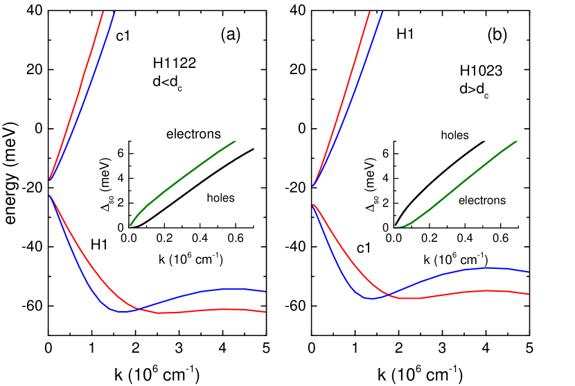
Let us now compare the experimental results obtained in the present paper both for the valence and conduction bands with the results calculated within framework of the kP model used in Ref. [14]. As before, we use here the six-band Kane Hamiltonian. The direct integration technique is applied to solve the Shrödinger equation as described in Ref. [26]. The other parameters were the same as in Refs. [27, 28]. As in the previous paper [14], the value of electric field serves as the fitting parameter, which provides the ratio between the hole densities in the split subbands, which is observed experimentally (see Fig. 15). It is approximately equal to mV for all the structures under study.
Let us now inspect the SO splitting of the conduction band. The calculated energy spectrum for the heterostructures with and is shown Fig. 16. The energy splitting as a function of the quasimomentum value is shown in the insets. It is seen that the splitting of the conduction band at low values, cm-1, is much larger than that of the valence band for . For , the situation is opposite; the valence band is split much stronger than the conduction band. Such relationships between splittings agree with the known result of symmetry analysis according to which for the c1 band and for the H1 band near . It should be emphasized that so low quasimomentum values correspond to very low carrier densities ( cm-2 and less) which are inaccessible experimentally. At larger quasimomentum values, these relationships are violated. The splitting values of c1 and H1 bands become close to each other. As seen from Fig. 16 the difference in the spin-orbit splitting for the valence and conduction bands does not exceed % for both heterostructures for cm-1 that corresponds to the actual carrier density range cm-2 [see Fig. 15].
In order to compare the results of the kP calculations with the experimental data, we have calculated the carrier density in the split subbands as and plotted the to and to ratios against the total carrier density in Fig. 15 by the dashed lines. It is evident that this model perfectly describes the data relating to the hole split subband and gives no agreement with the experimental results concerning the conduction band splitting. One of the reason why the used kP model fails when compared with the experiment is the fact that it ignores the asymmetry caused by the difference of the quantum well interfaces.
The role of the bulk inversion asymmetry of host crystals and interface inversion asymmetry in the SO splitting of the energy spectrum of 2D carriers was recently studied in Ref. [15]. Using the symmetry analysis and atomistic calculations the authors obtain surprising result. The asymmetry of CdTe/HgTe and HgTe/CdTe interfaces forming the CdTe/HgTe/CdTe quantum well results in the giant splitting of the energy spectrum; in the quantum wells of critical and close-to-critical width, , the splitting reaches a value of about meV.
Analogous calculations have been performed for our concrete case of (013) HgTe. The quantum well was supposed symmetric in the sense that no electric field was applied across the the well. The microscopical strain has been calculated in the atomistic valence force field model [29] and then incorporated in the tight-binding using standard procedure [30]. The tight-binding parameters used in calculations were obtained using procedure similar to that described in details in the Supplemental Material to Ref. [15] with the following modification. In Ref. [15] it was assumed that the change of the ionicity across the interface may be extracted from the atomic levels obtained in ab initio calculations. Instead, one may introduce more physical parameter, the change of electrostatic potential on anion across the interface, and fit this parameter to reproduce the expected properties of the interface. Tight-binding parameters in Ref. [15] correspond to the change of electrostatic potential on Te between the quantum well and barrier equal to eV, which is in accordance with ab initio calculations of HgTe/CdTe heteropair. For the interface between HgTe and Hg1-xCdxTe () alloy this parameter should be reduced to meV which leads to proportional reduction of the interface-induced spin splitting. The carrier densities in the subbands were calculated as , where is the area inside the Fermi contour, which is not a circle due to absence of axial symmetry. The results of calculations are depicted in Fig. 15 by the solid lines. One can see that the atomistic calculations describe the experimental SO splitting of the spectrum reasonably not only for the valence band but for the conduction band also. It is necessary to stress that no fitting parameters have been used in calculations.
VII Conclusion
We have studied the energy spectrum of the conduction and valence bands of 2D states in HgTe quantum well by means of magnetotransport measurements. The structures investigated have the width of the quantum wells close to the critical value where the spectrum changes from normal (at ) to inverted (at ). Simultaneous analysis of the SdH oscillations and Hall effect over the wide range of the electron and hole densities gives surprising result: the top of the valence band is strongly split by spin-orbit interaction while the splitting of the conduction band is absent, within experimental accuracy. This conclusion is supported by the results obtained in the tilted magnetic fields. The behavior of the SdH oscillations of electron conductivity with the changing tilt angle corresponds to the case when the orbital quantization is determined by normal component of the magnetic field, while the spin splitting is determined by the total field. The oscillations of the hole conductivity are totally determined by the normal component of the magnetic field indicating the SO interaction wins the Zeeman effect in the actual magnetic field range. Surprisingly, but such a ratio of the splittings is observed as for structures with normal spectrum () so for structures with inverted one (). These data are inconsistent with the kP calculations which take into account the Bychkov-Rashba effect caused by electric field directed across the quantum well. It is shown that the experimental results can be reasonably described within framework of the tight-binding method which properly takes into consideration the interface inversion asymmetry.
Acknowledgements.
We are grateful to I. V. Gornyi, S. A. Tarasenko, and O. E. Raichev for useful discussions. The work has been supported in part by the Russian Foundation for Basic Research (Grants No. 13-02-00322 and No. 15-02-02072) and by Act 211 Government of the Russian Federation, agreement No. 02.A03.21.0006. A.V.G. and O.E.R. gratefully acknowledge financial support from the Ministry of Education and Science of the Russian Federation under Projects No. 3.571.2014/K and No. 2457.References
- Gerchikov and Subashiev [1990] L. G. Gerchikov and A. Subashiev, Phys. Stat. Sol. (b) 160, 443 (1990).
- Bernevig et al. [2006] B. A. Bernevig, T. L. Hughes, and S.-C. Zhang, Science 314, 1757 (2006).
- M Schultz et al. [1996] M. M Schultz, F. Heinrichs, U. Merkt, T. Colin, T. Skauli, and S. Løvold, Semicond. Sci. Technol 11, 1168 (1996).
- Pfeuffer-Jeschke et al. [1998] A. Pfeuffer-Jeschke, F. Goschenhofer, S. J. Cheng, V. Latussek, J. Gerschütz, C. Becker, G. R. R., and G. Landwehr, Physica B 256-258, 486 (1998).
- Schultz et al. [1998] M. Schultz, U. Merkt, A. Sonntag, U. Rössler, R. Winkler, T. Colin, P. Helgesen, T. Skauli, and S. Løvold, Phys. Rev. B 57, 14772 (1998).
- Zhang et al. [2004] X. C. Zhang, K. Ortner, A. Pfeuffer-Jeschke, C. R. Becker, and G. Landwehr, Phys. Rev. B 69, 115340 (2004).
- Ikonnikov et al. [2011] A. V. Ikonnikov, M. S. Zholudev, K. E. Spirin, A. A. Lastovkin, K. V. Maremyanin, V. Y. Aleshkin, V. I. Gavrilenko, O. Drachenko, M. Helm, J. Wosnitza, M. Goiran, N. N. Mikhailov, S. Dvoretskii, F. Teppe, N. Diakonova, C. Consejo, B. Chenaud, and W. Knap, Semicond. Sci. Technol 26, 125011 (2011).
- Kozlov et al. [2011] D. A. Kozlov, Z. D. Kvon, N. N. Mikhailov, S. A. Dvoretskii, and J. C. Portal, Pis’ma Zh. Eksp. Teor. Fiz. 93, 186 (2011), [JETP Lett. 93, 170 (2011)].
- Kvon et al. [2011] Z. D. Kvon, S. N. Danilov, D. A. Kozlov, C. Zoth, N. N. Mikhailov, S. A. Dvoretskii, and S. D. Ganichev, Pis’ma Zh. Eksp. Teor. Fiz. 94, 895 (2011), [JETP Letters 94, 816 (2011)].
- Minkov et al. [2013] G. M. Minkov, A. V. Germanenko, O. E. Rut, A. A. Sherstobitov, S. A. Dvoretski, and N. N. Mikhailov, Phys. Rev. B 88, 155306 (2013).
- Zholudev [2013] M. Zholudev, Ph.D. thesis, University Montpellier 2, France (2013).
- Olshanetsky et al. [2012] E. Olshanetsky, Z. Kvon, N. Mikhailov, E. Novik, I. Parma, and S. Dvoretsky, Solid State Commun. 152, 265 (2012).
- Ortner et al. [2002] K. Ortner, X. C. Zhang, A. Pfeuffer-Jeschke, C. R. Becker, G. Landwehr, and L. W. Molenkamp, Phys. Rev. B 66, 075322 (2002).
- Minkov et al. [2014] G. M. Minkov, A. V. Germanenko, O. E. Rut, A. A. Sherstobitov, S. A. Dvoretski, and N. N. Mikhailov, Phys. Rev. B 89, 165311 (2014).
- Tarasenko et al. [2015] S. A. Tarasenko, M. V. Durnev, M. O. Nestoklon, E. L. Ivchenko, J.-W. Luo, and A. Zunger, Phys. Rev. B 91, 081302 (2015).
- Mikhailov et al. [2006] N. N. Mikhailov, R. N. Smirnov, S. A. Dvoretsky, Y. G. Sidorov, V. A. Shvets, E. V. Spesivtsev, and S. V. Rykhlitski, Int. J. Nanotechnology 3, 120 (2006).
- König et al. [2007] M. König, S. Wiedmann, C. Brüne, A. Roth, H. Buhmann, L. W. Molenkamp, X.-L. Qi, and S.-C. Zhang, Science 318, 766 (2007).
- Note [1] The details of capacitance measurements for HgTe quantum wells of the different widths are beyond the scope of this paper and will be published elsewhere.
- Kozlov et al. [2012] D. Kozlov, Z. Kvon, N. Mikhailov, and S. Dvoretsky, Pis’ma Zh. Eksp. Teor. Fiz. 96, 815 (2012), [JETP Letters 96, 730 (2012)].
- Minkov et al. [2015] G. M. Minkov, A. V. Germanenko, O. E. Rut, A. A. Sherstobitov, S. A. Dvoretski, and N. N. Mikhailov, Phys. Rev. B 91, 205302 (2015).
- Blatt [1968] F. J. Blatt, Physics of electronic conduction in solids (McGraw-Hill, US, 1968) p. 446.
- Note [2] Due to large noisiness at positive gate voltage we could not do this in the previous our paper [14]. The possible reason of the noise can be large resistance of the p-n junctions which are formed in the 2D gas under the gate electrode edge because these structures are of p type at .
- Raichev [2012] O. E. Raichev, Phys. Rev. B 85, 045310 (2012).
- Note [3] The detail analysis of electron-density dependence of g-factor in the structures with different width of quantum well are beyond the scope of this study and will be discuss in another paper.
- Note [4] We have plotted the ratio but not the value of SO splitting, , because to calculate from one needs the carriers effective mass which is known with some error.
- Larionova and Germanenko [1997] V. A. Larionova and A. V. Germanenko, Phys. Rev. B 55, 13062 (1997).
- Zhang et al. [2001] X. C. Zhang, A. Pfeuffer-Jeschke, K. Ortner, V. Hock, H. Buhmann, C. R. Becker, and G. Landwehr, Phys. Rev. B 63, 245305 (2001).
- Novik et al. [2005] E. G. Novik, A. Pfeuffer-Jeschke, T. Jungwirth, V. Latussek, C. R. Becker, G. Landwehr, H. Buhmann, and L. W. Molenkamp, Phys. Rev. B 72, 035321 (2005).
- Keating [1966] P. N. Keating, Phys. Rev. 145, 637 (1966).
- Jancu et al. [1998] J.-M. Jancu, R. Scholz, F. Beltram, and F. Bassani, Phys. Rev. B 57, 6493 (1998).