Topological Dirac Surface States and Superconducting Paring Correlations in PbTaSe2
Abstract
Superconductivity in topological band structures is a platform for realizing Majorana bound states and other exotic physical phenomena such as emergent supersymmetry. This potential nourishes the search for topological materials with intrinsic superconducting instabilities, in which Cooper pairing is introduced to electrons with helical spin texture such as the Dirac surface states of topological insulators, forming a time-reversal symmetric topological superconductor on the surface. We employ first-principles calculations and ARPES experiments to reveal that PbTaSe2, a non-centrosymmetric superconductor, possess a nonzero topological invariant and fully spin-polarized Dirac surface states. Moreover, we analyze the phonon spectrum of PbTaSe2 to show how superconductivity can emerge due to a stiffening of phonons by the Pb intercalation, which diminishes a competing charge-density-wave instability. Our work establishes PbTaSe2 as a stoichiometric superconductor with nontrivial topological band structure, showing it holds great promise for studying aspects of topological superconductors such as Majorana zero modes.
The interplay of topology and interacting electronic instabilities promises new ways to realize exotic physical phenomena. Majorana zero modes have been theoretically proposed to exist in the vortex core of chiral -wave superconductors TS-4 ; TS-1 ; TS-2 ; TS-3 ; TS-5 ; TS-6 ; TS-7 ; TS-8 ; TS-9 ; MF ; Das-1 ; Das-2 . These systems are topological due to the unconventional form of their order parameter, while their electronic band structure can be topologically trivial. Unfortunately, electrons rarely form a chiral -wave superconducting order in real materials. In a seminal work, Fu and Kane TS-2 realized that this can be overcome by interchanging the role of band structure and order parameter: Majorana zero modes can also appear when the topological surface states of a topological band structure are gapped due to ordinary -wave superconducting pairing. Multiple routes that have been proposed to realize this idea. One is to dope topological insulators (TIs), for example with copper atoms, giving rise to a transition temperature up to 3.8 K in Bi2Se3 TS-dop1 ; TS-dop2 ; TS-dop3 . However, this approach requires fine tuning of the chemical doping composition and also introduces in an uncontrollable way chemical disorder into the system. Besides, the nature of the resulting superconductivity remains unclear. Another approach is to artificially fabricate TI thin layers on top of a superconductor TScon . Helical pairing of Dirac surface states induced by the proximity effect has been observed experimentally TScon . However, complex interface interaction hinders a comprehensive understanding of the induced helical Cooper pairing and the superconducting gap drops steeply as the film thickness increases, which places stringent requirements on material synthesis. A way that overcomes these difficulties is to search for chemically stoichiometric superconductors which possess intrinsically topological surface states. To date, a stoichiometric superconductors with nontrivial topological band structure remains elusive in real materials.
In this paper, we use first-principles calculations and ARPES experiments to show that PbTaSe2, a recently discovered non-centrosymmetric superconductor PTS-exp , possesses a nonzero topological invariant and topologically protected surface states. PbTaSe2 is part of the family of layered transition metal dichalcogenide (TMD) superconductors, several of which show a competition between charge density wave (CDW) and superconducting order Klemm15 . For example, in CuxTiSe2 a superconducting dome appears to cover the quantum critical point at the Copper doping at which the CDW phase terminates CDW-4 . To understand how superconductivity can compete with the CDW instability in PbTaSe2, we performed a systematic phonon calculation, revealing a surprisingly strong electron-phonon coupling associated with the phonon mode that accompanies the vertical motion of Pb atoms. From the theoretically obtained electron-phonon coupling strength, we estimate the superconducting transition temperature to be 3.1 K, which agrees very well with our experimental measurements on single crystal PbTaSe2. Taken together the BCS-like superconductivity and Dirac surface states of PbTaSe2, our work established, for the first time, a material realization of a stoichiometric superconductor with topological band structure, providing a promising platform for studying exotic Majorana physics in condensed matter.
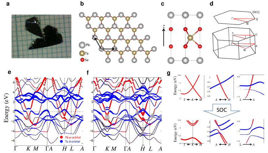
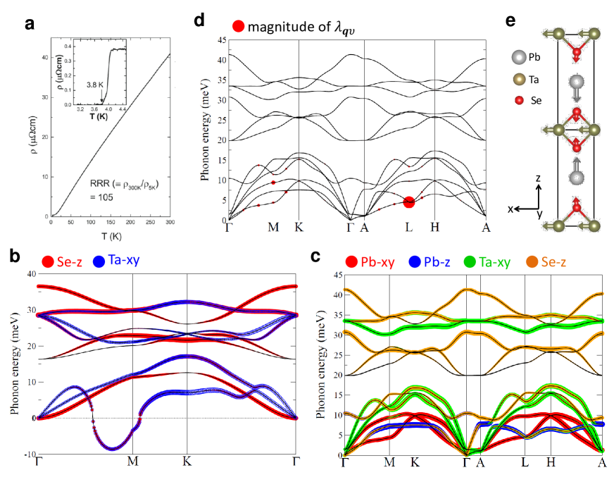
PbTaSe2 crystallizes in a structure of alternately-stacked hexagonal Pb and TaSe2 layers with space group Pm2 [Fig. 1(b)]. In a TaSe2 layer, a hexagonal Ta atomic plane is sandwiched by two hexagonal Se atomic planes, forming strong ionic bonds within a local trigonal structure. The lattice can also be viewed as a Pb layer intercalating two adjacent TaSe2 layers with Pb atoms sitting right above Se atoms. The Pb-Se bonds are relatively weak compared to the ionic Ta-Se bonds. This soft bonding plays an important role in the emergent superconductivity in PbTaSe2, as will be discussed later. For this study, PbTaSe2 single crystals were prepared by the chemical vapor transport (CVT) method, as shown in Fig. 1(a). We performed a transport measurement to verify the superconducting property of our samples. Figure 2(a) shows the resistivity curve displaying a clear superconducting transition at a temperature of 3.8 K, which is consistent with previous work on polycrystalline samples PTS-exp . Before discussing the superconductivity, we will present the bulk band structure obtained from first-principles calculations, which help us to understand the electronic structure of PbTaSe2.
Figure 1(d) shows the bulk band structure of PbTaSe2, calculated with the GGA method without the inclusion of spin-orbit coupling (SOC). The Pb -orbitals and Ta -orbitals dominate the bands around the Fermi energy , while Se 2 states are mainly below eV. The Pb -bands display electron-like band dispersion crossing with a bandwidth larger than 7 eV and form a Dirac bulk band dispersion at the point below the Fermi level [marked by gray areas in Fig. 1(d)]. In contrast to Pb -bands, Ta -orbitals exhibit a quite different behavior. The bands from Ta -orbitals split into two groups. The upper part lies at +3 eV above with a narrow bandwidth about 2 eV. The lower part displays hole-like band dispersion near and hybridizes strongly with Pb -bands around and points, leading to a complex band inversion feature around EF. Note that the band dispersion along –– ( = 0) is very different from that along –– ( = ), which indicates the coupling along direction can not be neglected even though the crystal is comprised of two-dimensional layers PTS-exp . This non-negligible interlayer coupling along the direction results in a surprising large electron-phonon coupling at , which will be discussed later. When SOC is turned on, the band crossings in Fig. 1(d) are gapped out [shown in the gray areas in Fig. 1(e) and the zoom-in shown in Fig.1 (F)] resulting in a continuous energy band gap spreading over the whole Brillouin zone (BZ). The band structure shows significant spin-orbit splitting due to the breaking of spatial inversion symmetry, except at the time-reversal invariant points (, , , and ) of the BZ.
To understand the emergence of superconductivity in PbTaSe2, we performed systematic calculations for the electron-phonon couplings. Since bulk 2-TaSe2 is known to exhibit a CDW instability below 122K CDW-1 ; CDW-2 , we first examine the stability of monolayer (ML) TaSe2 which is a building block of PbTaSe2. As shown in Fig. 2(b), the CDW instability is also seen in ML TaSe2. This instability results from the negative phonon energy of the mode that involves the horizontal motions of Ta and vertical motions of Se. Figure 2(c) shows the phonon spectrum of PbTaSe2. The CDW instability is eliminated by the intercalation of Pb layer. The phonon spectrum in Fig. 2(c) is displayed with the decomposition of atomic vibrations. The soft phonons stem mostly from the vibration of Pb atoms. The energy of the TaSe2-related phonons are pushed upward, partly due to the fact that the originally unstable phonons that involve the vertical motions of Se are stiffened by the Pb intercalation. We also note that the energy of phonons along – is very low, which implies that the Pb intercalation moves the system to the vicinity of another CDW instability that corresponds to the relative sliding between the TaSe2 slabs and the Pb sheets. This can be understood from the fact that the vertical bonding between TaSe2 and Pb-/ orbitals is very weak. In Fig. 2(d), the strength of electron-phonon coupling is visualized by red dots to reveal the -dependence of the electron-phonon coupling (). In our calculations, we find the total electron-phonon coupling to be . Using the the McMillan formula (please see Method section for details), the superconducting transition temperature is estimated to be 3.1 K. Our calculation agrees well with the results from the polycrystalline transport and specific heat experiments PTS-exp ( = 0.74 and 3.8 K) and our single crystal transport measurement, indicative of a BCS-like superconductivity in PbTaSe2. As shown in Fig. 2(d), the major contribution to the effective electron-phonon coupling comes from the phonons at . This wave vector does not lead to any apparent nesting of the band structure, which might be a reason why it does not trigger a CDW instability. It is also worth noting that this surprisingly large coupling strength takes place at , but not at . The reason for this difference lies in their influence on the Se-Ta-Se bond angle when the phonons vibrate with different wavevector . At , the two Pb atoms that sandwich the TaSe2 slab move in opposite directions [Fig. 2(e)], which greatly alters the Se-Ta-Se bond angle. At , on the other hand, the in-phase motions of these two Pb atoms in direction exert less influence on the Se-Ta-Se bond angle. In general, the bond angle has been shown to yield modifications of the electronic structures of TMDs TMD-2 . The enhanced change of the bond angle induced by the phonon at explains the large effective electron-phonon coupling.
From our analysis of the phonon spectrum, we conclude that the emergence of superconductivity in PbTaSe2 can be attributed to the disappearance of the CDW. This is a common physical mechanism in TMDs where the CDW and superconductivity compete with each other CDW-3 ; CDW-4 ; CDW-5 ; CDW-6 ; CDW-7 . Mostly, the CDW predominates in the competition for the gapping of Fermi surfaces. Superconductivity takes place when the CDW is suppressed by either pressurization or doping CDW-4 ; CDW-5 ; CDW-6 ; CDW-7 . In PbTaSe2, the phonon stiffening due to the Pb intercalation makes it energetically unfavorable to form the CDW order, opening the way for the transition into a superconducting phase.
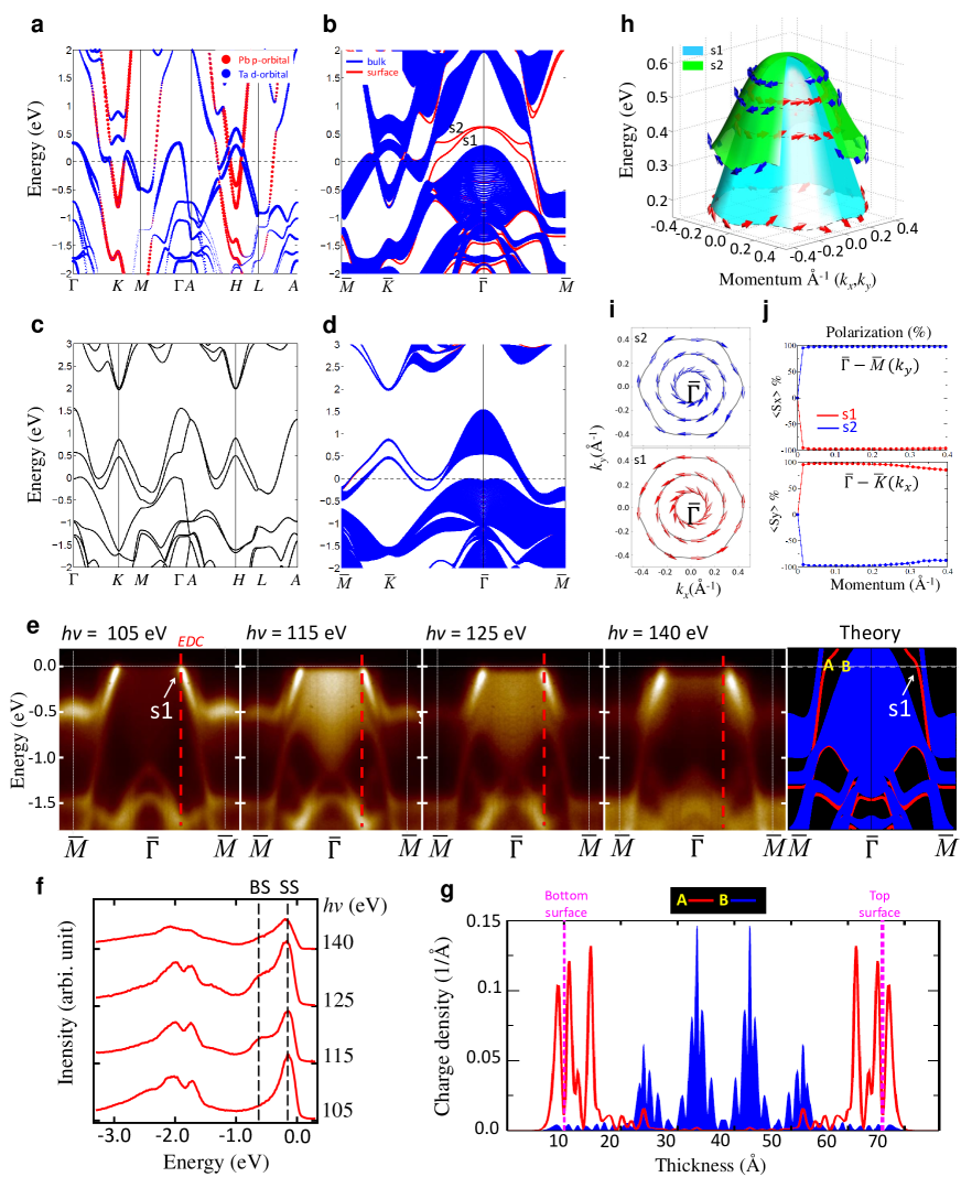
We now turn to the topological aspects of the electronic structure of PbTaSe2. In most typical three-dimensional TIs (such as Bi2Se3) the non-trivial topological bands originate from a band inversion induced by the SOC. The scenario in PbTaSe2 is rather different: an inverted band structure with two different orbital characters (Pb- and Ta-) exists in PbTaSe2 even without SOC as the highly dispersive Pb and Ta bands cross each other close to the Fermi level. The role of SOC in PbTaSe2 is to gap out the Dirac-like band dispersion at and other band crossings in the BZ [highlighted by gray shades in Fig. 1(f)], forming a continuous energy gap across the whole BZ. This is analogous to graphene in which the Dirac band at the point is gapped by the intrinsic SOC resulting in a quantum spin Hall phase, while the band structure is inverted at the points already in absence of SOC TI-G . Hence, even though PbTaSe2 has a metallic ground state, in presence of SOC the valence band remains separated from the conduction band by a continuous gap throughout the whole BZ. This allows to associate a well-defined topological invariant with the band structure TI-G . Since PbTaSe2 lacks inversion symmetry, the topological invariant cannot be computed via a parity analysis Z2-parity . For this reason, we calculated the index by the hybrid Wannier functions method Z2method . The topological number is extracted from a first-principles calculation using the Quantum Espresso code QE within the framework of the local density approximation (LDA) with SOC taken into account. A 303015 -grid is used to sample the BZ. The calculation shows a non-zero number (), indicating that PbTaSe2 is in the topological insulator phase.
Non-trivial topology of bulk band structure guarantees the existence of gapless surface states which are the hallmark of topological insulators. However, it is not clear a priori whether these surface states are observable if the band structure is metallic. The projection of the bulk bands in the surface BZ could cover the topological surface states. In the following we present first principle calculations and ARPES measurements showing that the surface states can indeed be observed in the (001) surface of PbTaSe2 thanks to the layered nature of the material. Figure 3(b) shows the surface band structure of PbTaSe2 calculated using a 6-unit-cell symmetric slab. Red and blue lines represent surface and bulk states projected onto the (001) surface [Fig. 1(c)], respectively. The gapless surface band lies in the continuous energy gap around the point. Along – and –, theres is only one surface band (red line) connecting the valence and conduction bands (blue lines), which is the signature of the nontrivial topological bands. Figure 3(e) shows ARPES spectra of PbTaSe2 taken with different photon energies along – direction. Near the intensity from the hole-like pocket varies prominently with photon energy, clearly indicating that it is part of the bulk band structure. In contrast, the band labelled s1 poking the Fermi level in between and shows a dispersion independent of photon energy, which evidences the surface nature of this band. We plot energy distribution curves [EDC, Fig. 3(f)] along the lines marked in Fig. 3(e). At different energies, the position of peak SS is unchanged, further proving the surface feature of band s1. By contrary the peak BS shows up at 115 eV but disappears at 105 and 140 eV, reflecting the bulk nature of this state. The ARPES results are remarkably consistent with theoretical prediction. Therefore, our ARPES measurements provide strong evidence for the existence of topological surface states in PbTaSe2. The calculated charge density distribution (in real space) of states A and B [marked in Fig. 3(e)] is shown in Fig. 3(g). Apparently, state A in band s1 is a typical surface state while state B is a bulk state.
A spin-momentum-locked helical spin-texture is one of most prominent characteristics of topological surface states. The cyan and green bell-like contours in Fig. 3(h) show a three-dimensional sketch of the surface states and around the point, respectively. The spin-textures can be seen clearly in the two-dimensional energy contours [Fig. 3(i)]. The in-plane spin-texture surrounding displays the right- and left-handed chirality for and , respectively, which is same as the surface spin-texture of Bi2Se3 TI-spin . The spin polarizations at and are opposite to each other, as dictated by time-reversal symmetry. Away from the point, the surface bands show hexagonal warping warping . This effect also leads to the finite out-of-plane spin component along the – () direction [Fig. 3(h)]. In contrast, the must be zero along – () because of the mirror symmetry of the crystal structure warping . We note that the spin polarization of surface states of PbTaSe2 around point is nearly 100 [Fig. 3(J)]. The in-plane spin polarization in PbTaSe2 remains nearly 100 along – even for a large momentum 0.3 Å-1, but decreases slightly along – () direction due to the emergence of the finite polarization from the hexagonal warping effect warping .
To highlight the critically important role of the Pb 6-orbitals in the formation of the non-trivial topological phase in PbTaSe2, we calculated the electronic structure of TaSe2 for comparison. Figure 3(c) shows bulk band structure of TaSe2. Contrary to PbTaSe2, which shows complex band inversion around [Fig. 3(a)], TaSe2 displays a clear separation between the valence band and the conduction band. Close to the there exist two large hole pockets, one at and the other one at . Those states are mainly derived from the Ta -orbitals. The band dispersion of TaSe2 is similar to the Ta part in the bulk band of PbTaSe2 [blue dots in Fig. 3(a)]. We also checked that the invariant in TaSe2 is trivial (). To further confirm this result, we performed slab calculation for TaSe2 (Fig.3(d)). It shows a clear energy gap with no surface band connecting the valence band and the conduction band, consistent the trivial index.
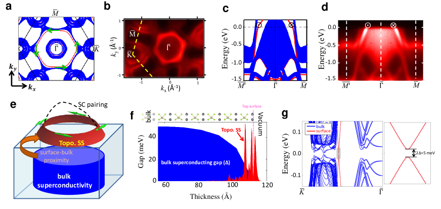
Let us finally discuss what promises the topological surface states of PbTaSe2 hold for observing Majorana zero modes in vortices. The two crucial ingredients needed are helical surface states that are well separated in momentum space from all bulk states and a fully gapped superconducting order. We have demonstrated that PbTaSe2 possesses the first ingredient. Figures 4(a), (b) show the calculated (001) Fermi surface and the ARPES measurement with 64 eV photon energy, respectively, clearly exposing the topological surface state. At Fermi level, there exist bulk band pockets surrounding at and , but the topological surface states encircling are not degenerate with these bulk bands, showing an isolated surface band with helical spin texture. As for the second ingredient, PbTaSe2 is intrinsically superconducting without the aid of doping or artificial heterostructures. Our phonon calculation illustrates the superconductivity of PbTaSe2 arises from an enormously enhanced electron-phonon coupling at and the estimated transition temperature is in accordance with the previous transport and specific heat measurements, indicating BCS-like Cooper pairing exists in this compound. When the temperature is below , the topological surface states can be superconducting as a consequence of surface-bulk proximity effect as schematically shown in Figs. 4(c-e). It is known that a superconducting spin-momentum-locked two-dimensional electron gas is topologically nontrivial with a helical (nodeless) Cooper pairing TScon . Recently it has been confirmed by the thermal conductivity and specific heat measurements R1 ; R2 that the superconducting gap of PbTaSe2 is nodeless, consistent with the picture of coexistence of BCS-type bulk superconducting states and helical surface superconducting states in PbTaSe2. Furthermore, the proximity-induced surface superconductivity in a bulk compound such as PbTaSe2 can be stronger than in an artificial TI-SC heterostructure since in an intrinsic superconductor there exists neither attenuation due to the finite thickness of the TI layer nor the complex interfacial condition TS-2 ; TScon . To show the superconducting proximity effect, we performed a simulation with an effective Hamiltonian for a 12-layer PbTaSe2 slab. In the model an on-site intra-orbital mean-field superconducting order parameter of -wave spin singlet type was introduced. In order to clearly demonstrate the proximity effect on the surface states the bare pairing potential is set to decay to zero in the surface layer [Fig. 4(f)]. Due to the extend of the surface states into the bulk, a superconducting gap is induced in surface bands. In our model we chose the bulk gap to be 50 meV, resulting in a proximitized nodeless gap of 5 meV on the surface states [Fig. 4(g)]. Thanks to this hybridization with bulk states and spin-momentum locking of the surface states, helical topological superconductivity can be induced on the surface TS-2 ; TScon . Therefore, PbTaSe2, an intrinsic superconductor with topological surface states, is a potential platform to study Majorana modes in the core of vortices PRL1 ; PRL2 ; PRB .
In summary, we have investigated electronic structure and electron-phonon coupling of PbTaSe2 via first-principles calculations and ARPES experiments. The CDW existing in TaSe2 is eliminated in PbTaSe2 by the intercalation of Pb layers. We also uncovered that the electron-phonon coupling is dominated by the mode at the point that accompanies the squeezing of the TaSe2 layer. The theoretical electron-phonon coupling strength is about 0.66 and estimates to be 3.1 K, consistent with our single crystal transport measurement ( 3.8 K). For the electronic structure, the Pb- orbitals hybridize strongly with Ta- orbitals at the and points, leading to a well-defined band-inverted energy gap and, consequently, a topologically nontrivial band structure. Slab calculations evidence the topological Dirac surface states with spin-momentum-locked spin texture. The calculated dispersion of the Dirac surface states is in good agreement with our ARPES measurement. Our work establishes that PbTaSe2, a stoichiometric compound, is a superconductor with nontrivial band topology, potentially providing a platform for studying Majorana bound states in vortices.
A very recent experimental work nodeless has shown that PbTaSe2 has a nodeless superconducting gap which is consistent with our theoretical discussion reported here.
I Methods
We computed electronic structures using the projector augmented wave method PAW-1 ; PAW-2 as implemented in the VASP VASP-1 ; VASP-2 ; VASP-3 package within the generalized gradient approximation (GGA) PBE schemes. Experimental lattice constants were used expstr . A 12124 MonkhorstPack -point mesh was used in the computations. The SOC effects are included self-consistently. The electron-phonon coupling is computed based on density functional perturbation theory DFPT implemented in the Quantum Espresso code QE , using
| (1) |
where is the density of states (DOS) at the Fermi level, and is the phonon frequency of mode at wave vector . The electron-phonon quasiparticle linewidth, , is given by
| (2) |
where is the energy of the KS orbital and the dynamical matrix reads
| (3) |
where represents the deformation potential at the small atomic displacement of the given phonon mode. M and denote the mass of the atom and the unit vector along , respectively. The critical temperature can then be estimated by the McMillan formula:
| (4) |
where
| (5) | |||||
| (6) | |||||
| (7) |
and is chosen to be 0.1 eV in the estimation of .
We simulated the superconducting state in a 12-layered PbTaSe2 slab. The non-superconducting slab Hamiltonian is constructed from the Wannier-function-based tight-binding model and the superconducting order parameter is chosen to be on-site intra-orbital spin singlet pairing among Pb and Ta -orbitals. For simplicity, we assumed equal gap amplitude for all orbitals. The boundary effect was considered by assuming the gap function in the -th layer to be
| (8) |
(). is chosen such that =50 meV at the center of the slab and is used. The choice of the gap function (8) produces a zero pairing at the boundaries ( and ).
ARPES measurements were performed at the liquid nitrogen temperature in the beamline I4 at the MAX-lab in Lund, Sweden. The energy and momentum resolution was better than 20 meV and 1 of the surface Brillouin zone (BZ) for ARPES measurements at the beamline I4 at the MAX-lab. Samples were cleaved in situ under a vacuum condition better than 1 10-10 torr. Samples were found to be stable and without degradation for a typical measurement period of 24 hours.
Single crystals of PbTaSe2 were grown by the CVT method using chlorine in the form of PbCl2 as a transport agent. For the pure synthesis of PbTaSe2, stoichiometric amounts of the elements (purity of Pb and Ta: 6N, of Se: 5N) were loaded into a quartz ampoule, which was evacuated, sealed and fed into a furnace (850) for 5 days. About 10 g of the prereacted PbTaSe2 were placed together with a variable amount of PbCl2 (purity 5N) at one end of another silica ampoule (length 30-35 cm, inner diameter 2.0 cm, outer diameter 2.5 mm). All treatments were carried out in an Argon box, with continuous purification of the Argon atmosphere resulting in an oxygen and water content of less than 1 ppm. Again, the ampoule was evacuated, sealed and fed into a furnace. The end of the ampoule containing the prereacted material was held at 850 , while the crystals grew at the other end of the ampoule at a temperature of 800 (corresponding to a temperature gradient of 2.5 K/cm) during a time of typically 1 week. Compact single crystals of sizes of up to 8 5 5 mm3 were obtained.
II Acknowledgements
T.R.C. acknowledges visiting scientist support from Princeton University. We gratefully acknowledge C. M. Polley, J. Adell, M. Leandersson, T. Balasubramanian for their beamline assistance at the Maxlab. We also thank Chen Fang, Ching-Kai Chiu and Andreas P. Schnyder for discussions.
References
- (1) A. Kitaev, AIP Conf. Proc. 1134, 22 (2009).
- (2) A. P. Schnyder, S. Ryu, A. Furusaki, and A. W. W. Ludwig, Phys. Rev. B 78, 195125 (2008).
- (3) L. Fu and C. L. Kane, Phys. Rev. Lett. 100, 096407 (2008).
- (4) X. L. Qi, T. L. Hughes, S. Raghu, and S. C. Zhang, Phys. Rev. Lett. 102, 187001 (2009).
- (5) M. Z. Hasan and C. L. Kane, Rev. Mod. Phys. 82, 30453067 (2010).
- (6) X.-L. Qi and S.-C. Zhang, Rev. Mod. Phys. 83, 10571110 (2011).
- (7) L. Fu and E. Berg, Phys. Rev. Lett. 105, 097001 (2011).
- (8) A. C. Potter and P. A. Lee, Phys. Rev. B. 83, 184520 (2011).
- (9) P. Hosur, P. Ghaemi, R. S. K. Mong, and A. Vishwanath, Phys. Rev. Lett. 107, 097001 (2011).
- (10) F. Wilczek, Nat. Phys. 5, 614 (2009).
- (11) C. Nayak, S. H. Simon, A. Stern, M. Freedman, and S. Das Sarma, Rev. Mod. Phys. 80, 1083 (2008).
- (12) J. D. Sau, R. M. Lutchyn, S. Tewari, and S. Das Sarma, Phys. Rev. Lett. 104, 040502 (2010).
- (13) L. A. Wray, S.-Y. Xu, Y. Xia, Y. S. Hor, D. Qian, A. V. Fedorov, H. Lin, A. Bansil, R. J. Cava, and M. Z. Hasan, Nature Phys. 6, 855 (2010).
- (14) Y. S. Hor, A. J. Williams, J. G. Checkelsky, P. Roushan, J. Seo, Q. Xu, H. W. Zandbergen, A. Yazdani, N. P. Ong, and R. J. Cava, Phys. Rev. Lett. 104, 057001 (2010).
- (15) S. Sasaki, M. Kriener, K. Segawa, K. Yada, Y. Tanaka, M. Sato, and Y. Ando, Phys. Rev. Lett. 107, 217001 (2011).
- (16) S.-Y. Xu, N. Alidoust, I. Belopolski, A. Richardella, C. Liu, M. Neupane, G. Bian, S.-H. Huang, R. Sankar, C. Fang, B. Dellabetta, W. Dai, Q. Li, M. J. Gilbert, F. Chou, N. Samarth, and M. Z. Hasan, Nature Phys. 10, 943 (2014).
- (17) M. N. Ali, Q. D. Gibson, T. Klimczuk, and R. J. Cava, Phys. Rev. B 89, 020505(R) (2014).
- (18) R. A. Klemm, Physica C 514, 86-94 (2015).
- (19) E. Morosan, H. W. Zandbergen, B. S. Dennis, J. W. G. Bos, Y. Onose, T. Klimczuk, A. P. Ramirez, N. P. Ong, and R. J. Cava, Nature Phys. 2, 544 (2006).
- (20) J. A. Wilson, F. J. Di Salvo, and S. Mahajan, Phys. Rev. Lett. 32, 882 (1974).
- (21) D. E. Moncton, J. D. Axe, and F. J. DiSalvo, Phys. Rev. Lett. 34, 734 (1975).
- (22) T.-R. Chang, H. Lin, H.-T. Jeng, and A. Bansil, Sci. Rep. 4, 6270 (2014).
- (23) D. E. Moncton, J. D. Axe, and F. J. DiSalvo, Phys. Rev. B 16, 801 (1977).
- (24) A. F. Kusmartseva, B. Sipos, H. Berger, L. Forr, and E. Tuti, Phys. Rev. Lett. 103, 236401 (2009).
- (25) B. Sipos, A. F. Kusmartseva, A. Akrap, H. Berger, L. Forr, and E. Tuti, Nature Mater. 7, 960 (2008).
- (26) P. Xu, J. O. Piatek, P.-H. Lin, B. Sipos, H. Berger, L. Forr, H. M. Rønnow, and M. Grioni, Phys. Rev. B 81, 172503 (2010).
- (27) C. L. Kane and E. J. Mele, Phys. Rev. Lett. 95, 146802 (2005).
- (28) L. Fu and C. L. Kane, Phys. Rev. B 76, 045302 (2007).
- (29) A. A. Soluyanov and D. Vanderbilt, Phys. Rev. B 83, 235401 (2011).
- (30) P. Giannozzi, S. Baroni, N. Bonini, M. Calandra, R. Car, C. Cavazzoni, D. Ceresoli, G. L Chiarotti, M. Cococcioni, I. Dabo, A. Dal Corso, S. de Gironcoli, S. Fabris, G. Fratesi, R Gebauer, U. Gerstmann, C. Gougoussis, A. Kokalj, M. Lazzeri, L. Martin-Samos, N. Marzari, F. Mauri, R. Mazzarello, S. Paolini, A. Pasquarello, L. Paulatto, C. Sbraccia, S. Scandolo, G. Sclauzero, A. P Seitsonen, A. Smogunov, P. Umari, and R. M Wentzcovitch, J. Phys. Condens. Matter 21, 395502 (2009).
- (31) Z. Sun, M. Enayat, A. Maldonado, C. Lithgow, E. Yelland, D. C. Peets, A. Yaresko, A. P. Schnyder, and P. Wahl, Nat Commun. 6, 6633 (2015).
- (32) D. Hsieh, Y. Xia, D. Qian, L. Wray, J. H. Dil, F. Meier, J. Osterwalder, L. Patthey, J. G. Checkelsky, N. P. Ong, A. V. Fedorov, H. Lin, A. Bansil, D. Grauer, Y. S. Hor, R. J. Cava, and M. Z. Hasan, Nature 460, 1101 (2009).
- (33) S. Basak, H. Lin, L. A. Wray, S.-Y. Xu, L. Fu, M. Z. Hasan, and A. Bansil, Phys. Rev. B 84, 121401 (2011).
- (34) M. X. Wang, et al., Preprint at arXiv:1511.02730.
- (35) G. M. Pang, et al., Preprint at arXiv:1512.02459.
- (36) J.-P. Xu, et al., Phys. Rev. Lett. 114, 017001 (2014).
- (37) P. Hosur, P. Ghaemi, R. S. K. Mong, and A. Vishwanath, Phys. Rev. Lett. 107, 097001 (2011).
- (38) C.-K. Chiu, P. Ghaemi, and T. L. Hughes, Phys. Rev. Lett. 109, 237009 (2012).
- (39) H.-H. Hung, P. Ghaemi, T. L. Hughes, and M. J. Gilbert, Phys. Rev. B 87, 035401 (2013).
- (40) M. X. Wang, Y. Xu, L. P. He, J. Zhang, X. C. Hong, P. L. Cai, Z. B. Wang, J. K. Dong, and S. Y. Li Phys. Rev. B 93, 020503(R) (2016).
- (41) P. E. Blchl, Phys. Rev. B. 50, 17953 (1994).
- (42) G. Kresse and J. Joubert, Phys. Rev. B. 59 1758 (1999).
- (43) G. Kress and J. Hafner, Phys. Rev. B. 48, 13115 (1993).
- (44) G. Kress and J. Furthmller, Comput. Mater. Sci. 6, 15 (1996)
- (45) G. Kress and J. Furthmller, Phys. Rev. B. 54 11169 (1996).
- (46) J. P. Perdew, K. Burke, and M. Ernzerhof, Phys. Rev. Lett. 77 3865 (1996).
- (47) R. Eppinga and G.A. Wiegers, Physica B and C 99, 121 (1980).
- (48) S. Baroni, S. de Gironcoli, A. Dal Corso, and P. Giannozzi, Rev. Mod. Phys. 73, 515 (2001).