Enhanced Photoabsorption from Cobalt Implanted Rutile TiO2 (110) Surfaces
Abstract
Present study investigates the photoabsorption properties of single crystal rutile TiO2 (110) surfaces after they have been implanted with low fluence of Cobalt ions. The surfaces, after implantation, demonstrate fabrication of nanostructures and anisotropic nano-ripple patterns. Creation of oxygen vacancies (Ti3+ states) as well as band gap modification for these samples is also observed. Results presented here demonstrate that fabrication of self organized nanostructures and development of oxygen vacancies, upon cobalt implantation, promote the enhancement of photoabsorbance in both UV (2 times) and visible (5 times) regimes. These investigations on nanostructured TiO2 surfaces can be important for photo- catalysis.
I Introduction
Studies of metal oxide semiconductors like TiO2, at nanoscales, have been of great interest for many years due to their numerous technological applications in photo- catalysis, solar cells, photovoltaics, magnetic storage media, waste water management, etc. Fuj ; Fuj1 ; Reg . TiO2 is a wide band gap semiconductor and under UV irradiation can produce hydroxyl radical (OH-) which act as a powerful oxidizing agent to disintegrate many organic pollutants dissolved in water Ino . However, due to its large band gap (3.2 eV for rutile TiO2) it absorbs visible light poorly, and thus has been nearly ineffective for visible light photo- catalysis. Various methods have been used to improve the photocatalytic activity of rutile TiO2, e.g. through dye sensitization, synthesis as thin films, formation of nanocrystals, incorporation of dopants by chemical methods, etc. Par1 ; Tan ; Wan . The enhancement of photocatalytic activity of rutile TiO2 by most of the above methods is however somehow limited, as organic dyes can become unstable at high temperature and the diffusion of dopants depend on the temperature and complexity of the chemical methods Cho ; Don ; Gut .
Ion implantation is an important technique for introducing dopants in the host lattice. Implantation sometimes leads to the development of nanostructures on the surfaces. Such fabrication of self organized nano-patterns have been observed on a variety of semiconductor and metal surfaces Val . These patterns develop due to the competition between the curvature dependent sputtering process, which erode the surface atoms, and various relaxation mechanisms Bra . During implantation of bi-atomic surfaces, preferential sputtering of low mass atoms can also take place which may lead to the development of vacancies as well as metal rich centers Sig .
The present study investigates the photoabsorption properties of rutile TiO2(110) surfaces after their implantation with Co ions. The results show formation of nanostructured patterns as well as creation of oxygen vacancies, or Ti3+ states, on the ion implanted surfaces. For these ion implanted surfaces an enhanced photoabsorption in UV as well as visible regimes is observed. The presented results demonstrate that development of self organized nanostructures, creation of vacancy states, and modification in band gap, upon Co ion implantation, leads to the observed increase in photoabsorption in TiO2(110).
II Experimental Details
Commercially available rutile single crystal TiO2 (110) substrates were irradiated with 200 keV cobalt ions, at room temperature, using 15 MV Pelletron Accelerator. The Co ions, incident along the substrate normal, were implanted in TiO2 at a fluence of . The flux of the ion source was . The range of Co atoms in TiO2 has been estimated to be 98 nm by SRIM Zie . Scanning Probe Microscope (SPM), Nanoscope V (Bruker), was utilized in tapping mode. For X-Ray Diffraction (XRD) measurements, a Bruker system equipped with Cu-Kα source ( 0.154 nm) was utilized. X-Ray Photoelectron Spectroscopy (XPS) studies were performed on a VG instrument which is equipped with a Concentric Hemispherical Analyzer and a dual x-ray source (Mg-Kα and Al-Kα). The resolution of the system is 0.9 eV. The spectra were acquired using an Mg-Kα source with a pass energy of 20 eV. Optical absorption studies were investigated using Shimadzu UV-vis spectrophotometer.
III Results and discussion
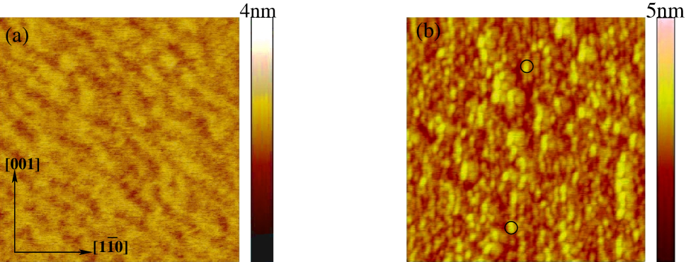
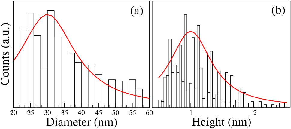
Morphological evolution of rutile TiO2 surfaces is shown in Fig. 1. High resolution image from a pristine TiO2 displays steps across the surface (Fig. 1(a)). The surface is smooth and shows a small mean roughness of 0.006 nm. Similar stepped morphologies with smooth surfaces have been earlier observed for TiO2 Ste . The implanted surface, however, is observed to be decorated with a large density () of nanostructures (outline for some are marked) in Fig. 1(b). The diameter (d) and height (h) distributions of these nanostructures, with an average and of 30 nm and 1 nm respectively, are shown in Fig. 2. These nanostructures predominantly display a 2-dimensional nature, with ratio being nearly 30.
An important consequence of the ion impact on single crystal substrates is the creation of adatoms and vacancy clusters Val . Along with the formation of well defined nanostructures, presence of ripple patterns can also be observed on the implanted TiO2 surfaces in Fig. 1(b). These ripples run along the [001] crystallographic direction and their ripple wave- vector is along [10] direction. The wavelength of these ripples is about 30 nm. The morphological evolution of the surfaces, during ion irradiation, predominantly happens due to various competing processes. Erosion and curvature dependent sputtering etc. induce surface instability whereas the process of surface diffusion of adatoms maintains the equilibrium Val .
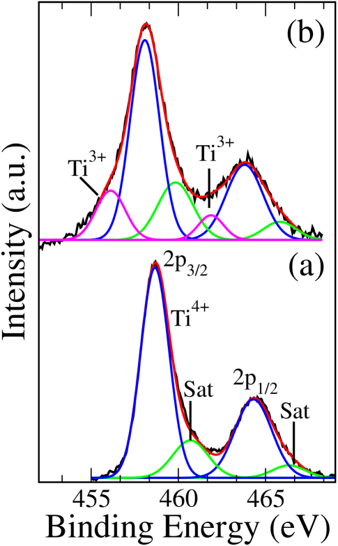
XPS is a very surface sensitive technique, with the photoelectron signal primarily coming from top 1 nm layer of the TiO2 Bri . Fig. 3 displays the Ti (2p) spectra for rutile TiO2 from the pristine as well as Co implanted TiO2. XPS from pristine surface shows the presence of 2p3/2 and 2p1/2 features at 458.6 eV and 464.3 eV, respectively. These features are related to the Ti4+ coordinated sites on the rutile TiO2 surface Sol ; Maj . Each of these states have an associated feature towards higher binding energy side (labeled as Sat). This is due to the shake up satellite from TiO2 Kha ; Mas . No sign of impurity or any Ti3+ vacancy state is observed for the pristine TiO2. Fig. 3(b) shows the XPS from the Co implanted TiO2. Here, in addition to Ti4+ related and shake- up- satellite related features, new features are also observed. These are due to the creation of oxygen vacancy states, or Ti3+ states, which get created during the ion irradiation of TiO2 Jeo . These Ti3+ related features for 2p3/2 and 2p1/2 states appear, respectively, at 456.1 eV and 461.8 eV in Fig. 3(b).
On hetroatomic crystals, preferential sputtering, during ion irradiation, usually occurs due to the difference in the binding energies of various atoms. This can sometimes lead to the development of metal rich centers as well as formation of vacancy states. After Co implantation in TiO2, the oxygen atoms get preferentially sputtered as compared to titanium atoms and lead to the development of Ti3+ states as seen in Fig. 3(b). With sputtering of oxygen atoms, the associated electrons go to empty 3d orbital of neighboring Ti atom forming the two Ti3+ sites. This leads to the creation of Ti rich zones which become the nucleation centers for the development of nanostructures Sol ; Maj . Room temperature DFT studies on rutile TiO2 (110) surface have shown that the diffusion barrier for vacancies as well as adatoms is lower along [001] crystallographic direction compared to the [10] direction Kol . The formation of anisotropic ripples running along [001], as observed here in Fig. 1(b), can be related to the non- symmetric diffusion barriers for Ti3+ vacancies. For metal substrates also similar results have been reported earlier Val ; Sha . The development of nanostructures as well anisotropic ripple patterns, on ion implanted TiO2 surfaces as observed in the present study, are crucially controlled by the preferential sputtering during irradiation and the non-symmetric diffusion of vacancies.
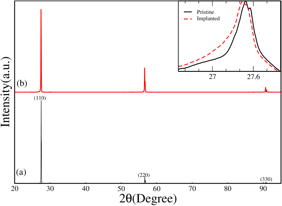
Fig. 4 displays the XRD results for TiO2 (110) samples both, prior to and after, implantation. The XRD diffraction pattern for pristine TiO2 shows a very prominent peak at 27.5∘ which corresponds to (110) plane of rutile TiO2 She1 . The other two lower intensity peaks at 56.7∘ and 90.7∘ can be attributed to (220) and (330) planes. Though all these features are observed after Co implantation in TiO2 also, they are shifted towards lower diffraction angle (inset Fig. 4 displays for (110) plane). These shifts suggest an increase in the interplanar lattice spacing after implantation. This can be caused by the substitution of some cobalt atoms in the TiO2 lattice, altering the lattice parameter of the latter due to the large ionic radii of cobalt atoms. This can also lead to the formation of compounds like Ti1-xCoxO2 Lau . Development of oxygen vacancies or Ti interstitials, during irradiation, can also cause modification in the lattice parameter as well as can generate lattice strain in the crystal Don1 . Inset of Fig. 4 also displays a slight increase in the FWHM of the (110) feature for the implanted sample as compared to the pristine. In addition, a prominent tailing effect is also observed in the lower angular region of this (110) feature (inset of Fig. 4). These are related to the phenomenon of diffuse scattering indicating loss in crystallinity and enhancement of defects in the implanted sample, that disturb the long range ordering of crystals Mor .
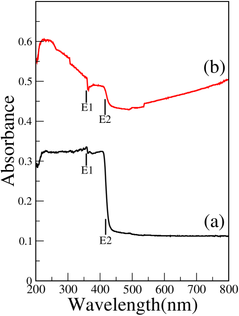
The photoabsorption studies in the UV-vis regime were performed for the pristine as well as Co implanted rutile TiO2 and the results are displayed in Fig. 5. The pristine surface exhibits two band edges as shown in Fig. 5(a). E1, is the direct band gap which arises due to optical transitions from O (2p) valance band to Ti (3d) conduction band while E2 is due to defects present in the crystal Rum . A significant enhancement in photoabsorption, about twice in UV regime and nearly five times in visible regime, has been observed from the ion implanted TiO2 surfaces (Fig. 5(b)). This enhancement of UV-vis photoabsorption after Co implantation, is significantly higher than observed earlier for other dopants Che . This enhancement can be related to the incorporation of cobalt atoms in TiO2 lattice which transfer their excess electrons to the conduction band of the host lattice via metal to conduction band charge transfer process Klo . In addition, formation of anisotropic nanostructures as well as creation of oxygen vacancies or Ti3+ states on the ion implanted TiO2 surfaces also promote absorbance Ser . The oxygen vacancies can act as trapping centers for electrons, with the mean free path of electrons getting significantly reduced. This inhibits the electron-hole recombination process and hence promotes the photoabsorbance Luo .
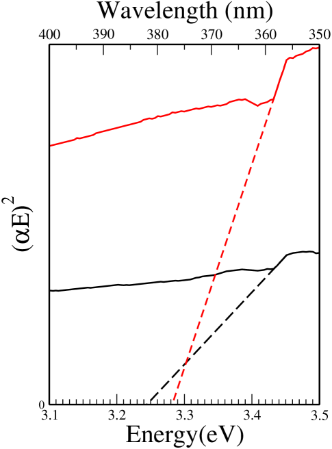
Photoabsorbance results of Fig. 5 were utilized to obtain the Tauc plots shown in Fig. 6. These have been utilized to study the band gap variation for both, pristine and Co implanted TiO2. The direct band gap of the pristine rutile TiO2 is observed to be at 3.25 eV. This is slightly higher than the theoretically predicted band gap (3.06 eV) Pas . After implantation this band gap increases very slightly to 3.28 eV. This redshift in direct band gap can be due to the quantum confinement effects, which according to the thermodynamic studies are pronounced for nanostructures of sizes smaller than 30 nm Sat .
IV Conclusion
In conclusion, we have investigated the photoabsorption properties of TiO2 surfaces after implantation with cobalt ions. Implantation leads to the fabrication of nanostructures as well as anisotropic ripple patterns. Development of oxygen vacancy states, or Ti3+ states, is also observed on ion implanted surfaces. These surfaces show an enhanced photoabsorption, nearly twice and five times, in UV and visible regimes, respectively. Formation of nanostructured patterns and development of oxygen vacancies, upon Co implantation, lead to the enhanced photoabsorption observed here. The nanostructured TiO2 surfaces investigated here can have wide applications in photo- catalysis.
Acknowledgment
We would like to acknowledge the help of Ramesh Chandra (IIT, Roorkee) for XRD measurements. Authors would also like to acknowledge the help of Devrani Devi during Implantation at IUAC and Santosh Kumar Choudhury for XPS experiments.
Figure caption
-
1.
AFM images of rutile TiO2 for (a) pristine, and after (b) cobalt implantation. Crystallographic directions of the surface are shown on pristine surface and remain same for the implanted sample. Few nanostructures, on the implanted surface, are marked with solid circles.
-
2.
(a) Diameter, and (b) Height distributions of nanostructures that develop on TiO2 surface after cobalt implantation. Solid lines represent Lorentzian fittings to the distributions.
-
3.
XPS Core level spectra of Ti (2p) of rutile TiO2 for (a) pristine surface, and after (b) cobalt implantation. Fittings of components are shown.
-
4.
X-Ray Diffraction (XRD) pattern of rutile TiO2 for (a) pristine and after (b) cobalt implantation. Inset shows the shift and peak broadening in TiO2 (110) peak after cobalt implantation.
-
5.
UV-vis absorbance spectra of rutile TiO2 for (a) pristine, and after (b) cobalt implantation.
-
6.
Tauc plots of rutile TiO2 for (a) pristine, and after (b) cobalt implantation. is the absorption coefficient while E is the energy of the variable source.
References
References
- (1) A. Fujishima, T. N. Rao, and D. A. Tryk, J. Photochem. Photobiol. C 1, 1 (2000).
- (2) A. Fujishima and K. Honda, Nature 238, 37 (1972).
- (3) B. O’Regan and M. Gratzel, Nature 353, 737 (1991).
- (4) T. Inoue, A. Fujishima, S. Konishi, and K. Honda, Nature 277, 637 (1979).
- (5) N. G. Park, J. Van de Lagemaat, and A. J. Frank, J. Phys. Chem. B 104, 8989 (2000).
- (6) S. Tanemura, L. Miao, W. Wunderlich, M. Tanemura, Y. Mori, S. Toh, and K. Kaneko, Sci. Technol. Adv. Mater. 6, 11 (2005).
- (7) J. Wang, D. N. Tafen, J. P. Lewis, Z. Hong, A. Manivannan, M. Zhi, M. Li, and N. Wu, J. Am. Chem. Soc. 131, 12290 (2009).
- (8) W. Choi, A. Termin, and M. R. Hoffmann, J. Phys. Chem. 98, 13669 (1994).
- (9) F. Dong, W. Zhao, and Z. Wu, Nanotechnology 19, 365607 (2008).
- (10) J. Gutierrez, A. Tercjak, and I. Mondragon, J. Am. Chem. Soc. 132, 873 (2010).
- (11) U. Valbusa, C. Boragno, and F. Buatier de Mongeot, J. Phys. Condens. Matter 14, 8153 (2002).
- (12) R. M. Bradley and J. M. E. Harper, J. Vac. Sci. Technol. A 6, 2390 (1988).
- (13) Peter Sigmund, Phys. Rev. 184, 383 (1969).
- (14) James F. Ziegler, M. D. Ziegler, and J. P. Biersack, Nucl. Instru. Meth. B 268, 1818 (2010).
- (15) Stefan Fischer, Andreas W. Munz, Klaus-Dieter Schierbaum, and Wolfgang Gopel, J. Vac. Sci. Tech. B 14, 961 (1996).
- (16) D. Briggs and M. P. Seah, Practical Surface Analysis: By Auger and X-Ray Photoelectron Spectroscopy, John Wiley and Sons, Ltd. (1978).
- (17) V. Solanki, S. Majumder, I. Mishra, S. R. Joshi, D. Kanjilal and S. Varma, Rad. Eff. Def. Solids 168, 518 (2013); S. Majumder, D. Paramanik, V. Solanki, I. Mishra, D. K. Avasthi, D. Kanjilal and S. Varma, Appl. Surf. Sci. 258, 4122 (2012).
- (18) S. Majumder, I. Mishra, U. Subudhi and Shikha Varma, Appl. Phy. Lett. 103, 063103 (2013); Vanaraj Solanki, Subrata Majumder, Indrani Mishra, P. Dash, C. Singh, D. Kanjilal and Shikha Varma, Jour. Appl. Phy. 115, 124306 (2014).
- (19) M. A. Khan, A. Kotani, and J. C. Parlebas, J. Phys. Condens. Matter. 3, 1763-1772 (1991).
- (20) Masaoki Oku, Hideyuki Matsuta, Kazuaki Wagatsuma, Yoshio Waseda, and Shigemi Kohiki, Journal of Electron Spectroscopy and Related Phenomena 105, 211-218 (1999).
- (21) H. Y. Jeong, J. Y. Lee, S. Y. Choi and J. W. Kim, Appl. Phys. Lett. 95, 162108 (2009).
- (22) M. Kolmer, A. A. Zebari, M. Goryl, F. Buatier de Mongeot, F. Zasadat, W. Piskorz, P. Pietrzyk, Z. Sojka, F. Kork, and M. Szymonski, Phys. Rev. B 88, 195427 (2013).
- (23) Shalik Ram Joshi, Trilochan Bagarti, and Shikha Varma, Surf. Sci. 641, 170 (2015).
- (24) Shengqiang Zhou, G. Talut, K. Potzger, A. Shalimov, J. Grenzer, W. Skorupa, M. Helm, J. Fassbender, E. izmar, S. A. Zvyagin, and J. Wosnitza, J. Appl. Phys. 103, 083907 (2008).
- (25) Laurianne Truffault, Minh-Tri Ta, Thierry Devers, Konstantin Konstantinov, Vale´ rie Harel, Cyriaque Simmonard, Caroline Andreazza, Ivan P. Nevirkovets, Alain Pineau, Olivier Veron, Jean-Philippe Blondeau, Material Research Bulletin 45, 527-535 (2010).
- (26) Dongwei Ma, Zhansheng Lu, Yanan Tang, Tingxian Li, Zhenjie Tang, and Zongxian Yang, Physics Letters A 378, 2570-2575 (2014).
- (27) M. Moreno, B. Jenichen, V. Kagnaner, W. Braun, A. Trampert, L. Daweritz, and K. H. Ploog, Phys. Rev. B 67, 235206 (2003).
- (28) A. K. Rumaiz, J. C. Woicik, E. Cockayne, H. Y. Lin, G. H. Jaffari, and S. I. Shah, Appl. Phys. Lett. 95, 262111 (2009).
- (29) Y. Chen, S. Zhang, Y. Yu, H. Wu, S. Wang, B. Zhu, W. Huang, and S. Wu, J. Dispersion Sci. Technol. 29, 245 (2008).
- (30) S. Klosek, and D. Raftery, J. Phys. Chem. B 105, 2815 (2001).
- (31) N. Serpone, J. Phys. Chem. B 110, 24287 (2006).
- (32) M. Luo, K. Cheng, W. Weng, C. Song, P. Du, G. Shen, G. Xu, and G. Han, J. Phys. D: Appl. Phys. 42, 105414 (2009); X. Pan, M. Q. Yang, X. Fu, N. Zhang, and Y. J. Xu, Nanoscale 5, 3601 (2013).
- (33) J. Pascual, J. Camassel, and H. Mathieu, Phys. Rev. B 18, 5606 (1978).
- (34) N. Satoh, T. Nakashima, K. Kamikura, and K. Yamamoto, Nature Nanotechnology 3, 106 (2008); H. Peng and J. Li, J. Phys. Chem. C 112, 20241 (2008).
