Transformation of spin current by antiferromagnetic insulators
Abstract
It is demonstrated theoretically that a thin layer of an anisotropic antiferromagnetic (AFM) insulator can effectively conduct spin current through the excitation of a pair of evanescent AFM spin wave modes. The spin current flowing through the AFM is not conserved due to the interaction between the excited AFM modes and the AFM lattice, and, depending on the excitation conditions, can be either attenuated or enhanced. When the phase difference between the excited evanescent modes is close to , there is an optimum AFM thickness for which the output spin current reaches a maximum, that can significantly exceed the magnitude of the input spin current. The spin current transfer through the AFM depends on the ambient temperature and increases substantially when temperature approaches the Neel temperature of the AFM layer.
Progress in modern spintronics critically depends on finding novel media that can serve as effective conduits of spin angular momentum over large distances with minimum losses Spintronics ; Spintronics1 ; Demidov . The mechanism of spin transfer is reasonably well-understood in ferromagnetic (FM) metals spincurrentGeneral ; metals and insulators Demidov ; spincurrentGeneral ; ferromagnets ; ferromagnets1 ; ferromagnets2 ; Demokritov , but there are only very few theoretical papers describing spin current in antiferromagnets (AFM) (see, e.g., Tserkovnyak2 ).
The recent experiments AFMExperiment ; AFMExperiment1 ; Saitoh have demonstrated that a thin layer of a dielectric AFM (NiO, CoO) could effectively conduct spin current. The transfer of spin current was studied in the FM/AFM/Pt trilayer structure (see Fig. 1). The FM layer driven in ferromagnetic resonance (FMR) excited spin current in a thin layer of AFM, which was detected in the adjacent Pt film using the inverse spin Hall effect (ISHE). It was also found in Saitoh that the spin current through the AFM depends on the ambient temperature and goes through a maximum near the Neel temperature . The most intriguing feature of the experiments was the fact that for a certain optimum thickness of the AFM layer ( nm) the detected spin current had a maximum AFMExperiment ; AFMExperiment1 , which could be even higher than in the absence of the AFM spacer AFMExperiment1 . The spin current transfer in the reversed geometry, when the spin current flows from the Pt layer driven by DC current through the AFM spacer into a microwave-driven FM material has been reported recently in Tserkovnyak1 .
The experiments AFMExperiment ; AFMExperiment1 ; Tserkovnyak1 ; Saitoh posed a fundamental question of the mechanism of the apparently rather effective spin current transfer through an AFM dielectric. A possible mechanism of the spin transfer through an easy-axis AFM has been recently proposed in Tserkovnyak2 . However, this uniaxial model can not explain the non-monotonous dependence of the transmitted spin current on the AFM layer thickness and the apparent “amplification” of the spin current seen in the experiments AFMExperiment ; AFMExperiment1 performed with the bi-axial NiO AFM layer AFMNuclScat .
In this Letter, we propose a possible mechanism of spin current transfer through anisotropic AFM dielectrics, which may explain all the peculiarities of the experiments AFMExperiment ; AFMExperiment1 ; Tserkovnyak1 . Namely, we show that the spin current can be effectively carried by the driven evanescent spin wave excitations, having frequencies that are much lower than the frequency of the AFM resonance. We demonstrate that the angular momentum exchange between the spin subsystem and the AFM lattice plays a crucial role in this process, and may lead to the enhancement of the spin current inside the AFM layer.
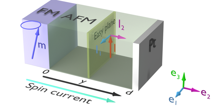
We consider a model of a simple AFM having two magnetic sublattices with the partial saturation magnetization . The distribution of the magnetizations of each sublattice can be described by the vectors and , . We use a conventional approach for describing the AFM dynamics by introducing the vectors of antiferromagnetism () and magnetism () sigmamodel ; sigmamodelAfleck ; Kosevich ; IvanovSatoh :
| (1) |
Assuming that all the magnetic fields are smaller then the exchange field and neglecting the bias magnetic field, that is used to saturate the FM layer, the effective AFM Lagrangian can be written as sigmamodel ; Kosevich ; IvanovSatoh :
| (2) |
Here , is the gyromagnetic ratio, is the speed of the AFM spin waves ( km/s in NiO), and is the energy of the anisotropy, defined by the matrix of the anisotropy fields with the diagonal components ( is the anisotropy constant along the -th axis). The equilibrium direction of the AFM vector lies along the axis.
The exchange coupling between the FM and AFM layers is modeled in Eq. (2) by the surface energy term , where is the surface energy density, is the unit vector of FM layer magnetization. We assumed that the net magnetization of the AFM at the FM/AFM interface layer could be partially non-compensated, and this “non-compensation” is characterized by a dimensionless parameter ().
The dynamical equation for the AFM vector l follows from the Lagrangian Eq. (2) and can be written as
| (3) |
where is the phenomenological damping parameter equal to the AFM resonance linewidth (GHz for NiO Sievers ). Note, that the damping-related decay length nm is much larger than the typical AFM thickness. Therefore, below we shall neglect damping except in Fig. 4, where the comparison of AFM spin currents in conservative and damped cases is presented. The matrix and , , are the frequencies of the AFM resonance. In the case of NiO the two AFM resonance frequencies are substantially different: GHz and THz AFMNuclScat . We shall show below that the difference between the AFM resonance frequencies is crucially important for the spin current transfer through the AFM.
The driving force in Eq. (3) , localized at the FM/AFM interface, describes AFM excitation by the precessing FM magnetization. In the absence of this term Eq. (3) describes two branches of the eigen-excitations of the AFM with dispersion relations . These propagating AFM spin waves have minimum frequencies which are much higher than the excitation frequency ( GHz in Ref. AFMExperiment ) and, therefore, can not be responsible for the spin current transfer.
The presence of the FM layer, however, qualitatively changes the situation, as the driving force excites evanescent AFM spin wave modes at the frequency of the FM layer resonance (FMR), that is well below any of the AFMR frequencies . The profiles of the evanescent AFM modes can be easily found from Eq. (3):
| (4) |
where is the excitation frequency,
| (5) |
is the penetration depth for the -th evanescent mode, and complex coefficients , are determined by the boundary conditions at the FM/AFM and AFM/Pt interfaces. The interfacial driving force excites the AFM vector at the FM/AFM interface:
| (6) |
The complex amplitudes and depend on the vector structure of the magnetization precession in the FM layer (see Supplementary Materials for details), which opens a way to experimentally control the input spin current in the AFM, and to directly verify our theoretical predictions. Thus, if the FM layer is magnetized along one of the AFM anisotropy axes , the microwave magnetization component along that axis will be zero and the corresponding complex amplitude in Eq. (6) will vanish. On the other hand, if the FM layer is magnetized along the AFM equilibrium axis , both amplitudes and will be non-zero with the phase shift between them.
At the AFM/Pt interface () we adopt a simple form of the boundary conditions that were used previously for the description of spin current at the AFM/Pt Bratas and FM/Pt Tserkovnyak interfaces:
| (7) |
where is the current of the -component of the spin angular momentum and is the corresponding angular momentum density inside the AFM:
| (8) |
and is a dimensionless constant having magnitude in the range from 0 to 1 and being physically determined by the spin mixing conductance at the AFM/Pt interface Tserkovnyak . The case corresponds to the conservative situation of a complete absence of the angular momentum flux, while the case describes a “transparent” boundary, when the angular momentum freely moves across the AFM/Pt boundary without any reflection.
Using Eqs. (8), the boundary conditions Eq. (7) can be rewritten as explicit conditions on the vector of antiferromagnetism as . This equation and Eq. (6) allow one to find all four coefficients , in Eq. (4), and one can find the explicit expression for the spin current inside the AFM layer:
| (9) |
where
| (10) |
Here and . Eq. (9) is the central result of this paper that allows one to find the spin current carried by the evanescent spin wave modes in an AFM layer. inline]Below we shall analyze the main features of the spin current transfer through an AFM dielectric that are described by Eq. (9).
Using Eq. (9), we estimated the ISHE voltage SaitohVoltage for an FM/AFM/Pt structure (NiFe/ NiO/Pt structure) with the AFM layer having thickness that is smaller than the penetration depths of both evanescent AFM modes for the following parameters: , erg/cm2 Celinski , FM precession angle , Pt spin Hall angle AFMExperiment1 , Pt length mm AFMExperiment , Pt thickness nm. We obtained mV for the fully uncompensated AFM () and nV for the fully compensated AFM (). The first value is close to the ISHE voltage measured in Ref. AFMExperiment . A partial interfacial magnetization of the antiferromagnetic NiO in this case is confirmed by the XRD scan performed in AFMExperiment . The calculated ISHE voltage for the compensated AFM is closer to the experimental value obtained in Ref. AFMExperiment1 .
Now we shall analyze the main features of the spin current transfer through an AFM dielectric that are described by Eq. (9). First, one can see that the spin current is proportional to the product of the amplitudes of both excited evanescent spin wave modes, and this current is completely absent if only one of the modes is excited. This is explained by the fact that each of the modes Eq. (4) is linearly polarized, and, therefore, can not alone carry any angular momentum.
Second, the spin current in the AFM layer depends on the position inside the AFM layer, i.e., it is not conserved. This is a direct consequence of the assumed bi-axial anisotropy of the AFM material, which allows for the transfer of the angular momentum between the spin sub-system and the crystal lattice of the AFM layer. This effect is a magnetic analogue of the optical effect of birefringence biref , where the spin angular momentum of light is dynamically changed during its propagation in a birefringent medium.
In the case of a uniaxial anisotropy Tserkovnyak2 () Eq. (9) can be simplified to
| (11) |
and the spin current is conserved across the whole AFM layer.
Another peculiarity of Eq. (9) and Eq. (11) is that the spin current depends on the phase shift between the two excited evanescent AFM spin wave modes and : , where . The maximum spin current at a given position inside the AFM layer is achieved at . Since the AFM phase shift , in general, depends on the position inside the AFM layer, for any particular thickness of the AFM layer it is possible to choose the excitation phase shift that would maximize the output spin current , while the input spin current could be quite low. In such a case the additional angular momentum is taken from the crystal lattice of the AFM. This shows that, in principle, the AFM dielectrics can serve as “amplifiers” of a spin current.
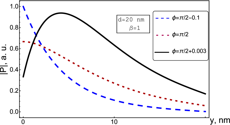
Fig. 2 shows the spatial profiles of the spin current density in a relatively thick AFM layer (thickness nm). This dependence is drastically different for different phase shifts between the excited evanescent spin wave modes. While for the spin current exponentially and monotonically decays inside the AFM layer (dashed blue line in Fig. 2), for (solid black line in Fig. 2) it initially increases at relatively small due to the angular momentum flow from the AFM crystal lattice to its spin subsystem. At larger values of , the spin current decays exponentially due to the decay of the excited evanescent spin wave modes.
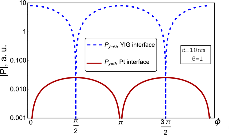
Fig. 3 demonstrates the dependences of the spin current on the phase shift at both interfaces FM/AFM (input spin current) and AFM/Pt (output spin current). It is clear from Fig. 3 that the output spin current is shifted by relative to the input spin current, and, for the phase shift , the output spin current could have a maximum magnitude when the input spin current is almost completely absent. This means, that at such a value of the phase shift between the evanescent spin wave modes practically all the output spin current is generated as a result of interaction between the magnetic subsystem of the AFM layer and its crystal lattice. Thus, the AFM layer acts as a source of the spin current. On the other hand, at the phase shift of or , the situation is opposite, as the input spin current is practically lost inside the AFM, and the AFM layer acts as a spin current sink.
Thus, we showed, that a thin layer of AFM, driven by a constant flow of microwave energy from the FM layer, is able to transform the angular momentum of a crystal lattice into the spin current and vice versa. The described transfer of the angular momentum from the lattice to the spin system has a simple analog not only as a birefringence in optics, but also in mechanics: a mechanical oscillator which consists of a mass suspended on two perpendicular springs with different stiffness attached to a fixed rectangular frame. The displacement of the mass from its equilibrium position in the frame center along the direction of one of the orthogonal springs results in the linearly polarized oscillations along this direction, without any transfer of the angular momentum from the frame to the oscillating mass. In contrast, the linear displacement of the mass in a diagonal direction results in the rotation of the mass around its equilibrium position, and the angular momentum necessary for this rotation is taken from the frame (see animations in Suppl. Mater.).
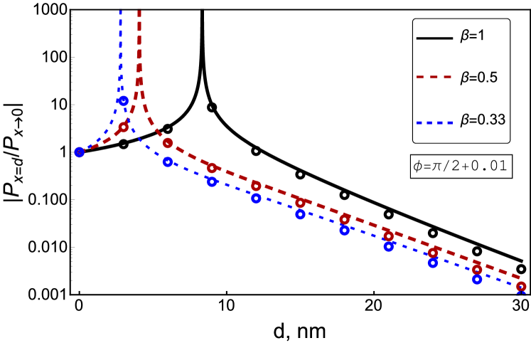
The ratio of the output spin current to the input one (the spin current transfer factor) is shown in Fig. 4 for different values of the constant , i.e., for the different values of the spin mixing conductance at the AFM/Pt interface. This dependence has a sharp maximum at the thickness of a few nanometers, where the input current is rather low, and the AFM layer acts as a source of a spin current. With the further increase of the AFM layer thickness the transfer ratio is exponentially decreasing, while the position of the maximum shifts to the right with the increase of the spin mixing conductance at the AFM/Pt interface. As one can see from Fig. 4, the presence of the damping has little influence on the spin current, because the spatial decay of the amplitudes due to the evanescent character of the modes is dominant.
The above presented results were obtained for the parameters of bulk NiO at low temperature. However, it is well known that such important parameters of AFM substances as the anisotropy constants and Neel temperature in thin AFM films could be substantially smaller than in bulk crystals (see, e.g., Alders ). Thus, the penetration depths of the evanescent spin wave modes Eq. (5), determined at a given driving frequency by the AFM anisotropy constants, would significantly depend on the thickness and the temperature of the AFM layer. Particularly, with the increase of temperature the AFMR frequencies would decrease and approach zero at the Neel temperature Sievers . In accordance with Eq. (5), this means that the penetration depth of the evanescent spin wave modes will increase substantially when the temperature approaches the Neel temperature of the AFM layer. This increase of the spin current transferred through the AFM layer is clearly seen in the experiments Saitoh .
In conclusion, we demonstrated that the spin current can be effectively transmitted through thin dielectric AFM layers by a pair of externally excited evanescent AFM spin wave modes. In the case of AFM materials with bi-axial anisotropy the transfer of angular momentum between the spin subsystem and the crystal lattice of the AFM can lead to the enhancement or decrease of the transmitted spin current, depending on the phase relation between the excited evanescent spin wave modes. Our results explain all the qualitative features of the recent experiments AFMExperiment ; AFMExperiment1 ; Tserkovnyak1 ; Saitoh , in particular, the existence of an optimum thickness of the AFM layer, for which the output current could reach a maximum value which is higher than the spin current magnitude in the absence of the AFM spacer, and the increase of the transmitted spin current at the temperatures close to the Neel temperature of the AFM layer.
This work was supported in part by the Grant ECCS-1305586 from the National Science Foundation of the USA, by the contract from the US Army TARDEC, RDECOM, by DARPA MTO/MESO grant N66001-11-1-4114 and by the Center for NanoFerroic Devices (CNFD) and the Nanoelectronics Research Initiative (NRI).
References
- (1) S.A. Wolf, D.D. Awschalom, R.A. Buhrman, J.M. Daughton, S. von Molnar, M.L. Roukes, A.Y. Chtchelkanova, and D.M. Treger, Science, 294, 1488 (2001).
- (2) S. Maekawa, Concepts in Spin Electronics (Oxford Univ. Press, 2006), Ch. 7 and 8.
- (3) V.E. Demidov, S. Urazhdin, H. Ulrichs, V. Tiberkevich, A. Slavin, D. Baither, G. Schmitz, and S.O. Demokritov, Nature Mater. 11, 1028 (2012).
- (4) Y. Kajiwara, K. Harii, S. Takahashi, J. Ohe, K. Uchida, M. Mizuguchi, H. Umezawa, H. Kawai, K. Ando, K. Takanashi, S. Maekawa, and E. Saitoh, Nature 464, 262 (2010).
- (5) T. Valet and A. Fert, Phys. Rev. B 48, 7099 (1993).
- (6) J.E. Hirsch, Phys. Rev. Lett. 83, 1834 (1999).
- (7) Z. Li and S. Zhang, Phys. Rev. Lett. 92, 207203 (2004).
- (8) M. Tsoi, V. Tsoi, J. Bass, A.G.M. Jansen, and P. Wyder, Phys. Rev. Lett. 89, 246803 (2002).
- (9) H. Kurebayashi, O. Dzyapko, V. E. Demidov, D. Fang, A. J. Ferguson, S. O. Demokritov, Nature Mat. Lett, 10, 660 (2011).
- (10) S. Takei, T. Moriyama, T. Ono, and Y. Tserkovnyak, Phys. Rev. B 92, 020409(R) (2015).
- (11) H. Wang, C. Du, P.C. Hammel, and F. Yang, Phys. Rev. Lett. 113, 097202 (2014).
- (12) C. Hahn, G. de Loubens, V.V. Naletov, J.B. Youssef, O. Klein, and M. Viret, Europhys. Lett. 108, 57005 (2014).
- (13) Z. Qiu, D. Hou, K. Uchida, and E. Saitoh, arXiv:1505.03926 (2015).
- (14) T. Moriyama, S. Takei, M. Nagata, Y. Yoshimura, N. Matsuzaki, T. Terashima, Y. Tserkovnyak, and T. Ono, Appl. Phys. Lett. 106, 162406 (2015).
- (15) M.T. Hutchings and E.J. Samuelsen, Phys. Rev. B 6, 3447 (1972).
- (16) A. Andreev and V. Marchenko, Sov. Phys. Usp. 23, 21 (1980).
- (17) I. Affleck and R.A. Weston, Phys. Rev. B 45, 4667 (1992).
- (18) A. M. Kosevich, B. A. Ivanov, A. S. Kovalev, Physics Reports, 194, 117-238 (1990)
- (19) T. Satoh, S.-J. Cho, R. Iida, T. Shimura, K. Kuroda, H. Ueda, Y. Ueda, B.A. Ivanov, F. Nori, and M. Fiebig, Phys. Rev. Lett. 105, 077402 (2010).
- (20) A.J. Sievers and M. Tinkham, Phys. Rev. 129, 1566 (1963).
- (21) R. Cheng, J. Xiao, Q. Niu, and A. Brataas, Phys. Rev. Lett. 113, 057601 (2014).
- (22) Y. Tserkovnyak, A. Brataas, and G.E.W. Bauer, Phys. Rev. Lett. 88, 117601 (2002).
- (23) H. Nakayama et al., Phys. Rev. B, 85, 144408 (2012).
- (24) B. K. Kuanr, R. E. Camley, and Z. Celinski, Journal of Appl. Phys. 93, 7723, (2003).
- (25) M. Born, E. Wolf, Principles of Optics: Electromagnetic Theory of Propagation, Interference and Diffraction of Light (Cambridge University Press, 1997), Ch. 9.
- (26) D. Alders, L.H. Tjeng, F.C. Voogt, T. Hibma, G.A. Sawatzky, C.T. Chen, J. Vogel, M. Sacchi, and S. Iacobucci, Phys. Rev. B 57, 11623 (1998).