Spin-orbit torque switching without external field with a ferromagnetic exchange-biased coupling layer
Abstract
Magnetization reversal of a perpendicular ferromagnetic free layer by spin-orbit torque (SOT)Miron et al. (2011); Liu et al. (2012a, b); Fan et al. (2014) is an attractive alternative to spin-transfer torque (STT) switchingSlonczewski (1996); Berger (1996) in magnetic random-access memory (MRAM) where the write process involves passing a high current across an ultrathin tunnel barrierIkeda et al. (2010). A small symmetry-breaking bias field is usually needed for deterministic SOT switching but it is impractical to generate the field externally for spintronic applications. Here, we demonstrate robust zero-field SOT switching of a perpendicular \ceCo90Fe10 (\ceCoFe) free layer where the symmetry is broken by magnetic coupling to a second in-plane exchange-biased \ceCoFe layer via a nonmagnetic \ceRu spacerParkin et al. (1990). The preferred magnetic state of the free layer is determined by the current polarity and the nature of the interlayer exchange coupling (IEC). Our strategy offers a scalable solution to realize bias-field-free SOT switching that can lead to a generation of SOT-based devices, that combine high storage density and endurance with potentially low power consumption.
For memory applications, a storage layer with perpendicular magnetic anisotropy (PMA) is preferred because it offers higher storage density, better thermal stability and lower power consumption than a layer with easy plane anisotropyMangin et al. (2006); Ikeda et al. (2010). However, deterministic SOT switching of a perpendicularly magnetized nanomagnet usually relies on an external magnetic field to break the symmetryMiron et al. (2011); Liu et al. (2012a, b). SOT switching without an external field has recently been demonstrated in systems with lateral asymmetryYu et al. (2014) or with tilted magnetic anisotropyYou et al. but neither of these schemes is easily scalablenot .
Here, we combine two concepts that have been developed in the context of modern hard-disc read heads and magnetic tunnel junctions: exchange biasNogués and Schuller (1999) and exchange coupling across a thin spacerParkin et al. (1990) to achieve scalable SOT switching without an external field. Using a stack based on a perpendicularly-magnetized \ceCo90Fe10 (\ceCoFe) free layer sandwiched between a \cePt underlayer and a \ceRu overlayer, we show that the free layer can be deterministically switched by SOT from the \cePt. The symmetry-breaking issue is resolved by exchange coupling the free layer, via a \ceRu spacer, to an in-plane exchange biased \ceCoFe pinned layer.
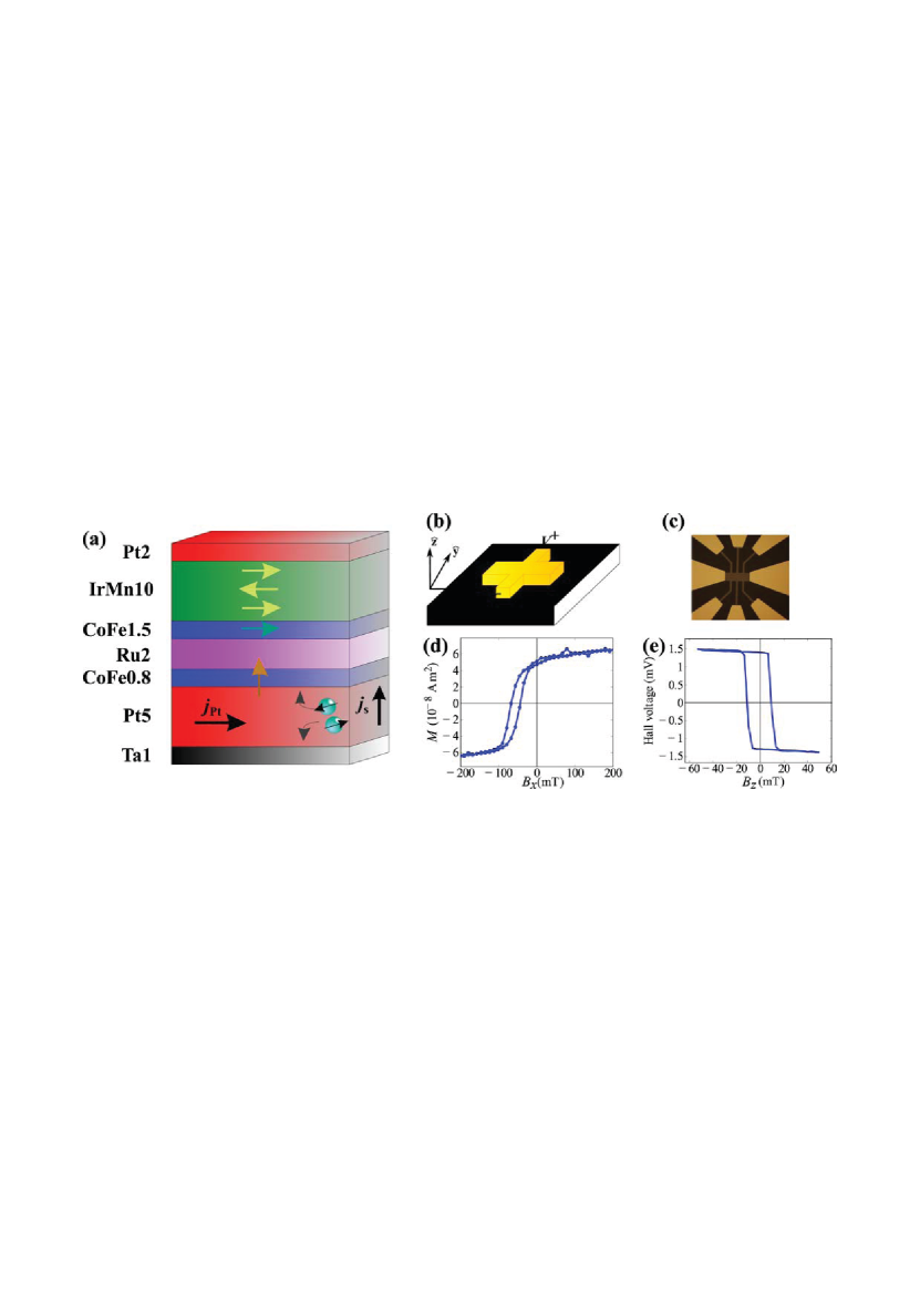
Our stacks, illustrated in Figure 1(a), consist of \ceTa()/\cePt()/\ceCoFe()/\ceRu()/\ceCoFe()/\ceIrMn()/\cePt() (thicknesses in nanometre). The \ceRu has been selected for the spacer because it provides the strongest IECParkin (1991) and together with the \cePt underlayer, it improves the PMA of the \ceCoFe free layer. A series of control samples with varying \cePt thickness: \ceSi/\ceSiO2(substrate)//\ceTa()/\cePt()/\ceCoFe()/\ceRu() were also grown. All stacks are patterned into micron-sized Hall bars with a channel of width and length ranging from to . Figure 1(b) shows a device schematic with the definition of the coordinate system, while Figure 1(c) is an optical micrograph of a typical Hall bar. All patterned devices are vacuum annealed at for in to set the exchange-bias direction. The top \ceCoFe layer is pinned along the -axis, with the magnetization parallel (anti-parallel) to the current when the annealing field is directed along (). An exchange-bias field of on a blanket film with is evidenced by magnetization curve in a field , plotted in Figure 1(d). Figure 1(e) shows the anomalous Hall effect (AHE) voltage, as a function of out-of-plane field for a Hall bar with . is measured with an applied current of which corresponds to a current density of in the bottom \cePt layer.
With the convention defined in Figure 1(b), the spin Hall effect (SHE)Dyakonov and Perel (1971); Hirsch (1999) in \cePt due to a charge current along , generates a spin accumulation polarised along at the top interface of the \cePt layer. The pure spin current, , relaxing within the adjacent \ceCoFe free layer with moment , exerts a Slonczewski-like SOT directed along and a field-like SOT along . The magnitudes of the two orthogonal SOT components are parametrised by the real and the imaginary parts of the complex spin-mixing conductance at the \cePt/\ceCoFe interfaceBrataas et al. (2000). Given the micrometric dimensions of our devices, a macrospin model is inapplicable and the switching should be described in terms of domain nucleation followed by thermally-assisted SOT-driven domain wall propagation.Lee et al. (2014) Efficient SOT-driven domain wall motion in a PMA material can be obtained when the wall assumes a Néel configuration (where the magnetization rotates in the plane) rather than a Bloch one (where the magnetization rotates in the plane).Haazen et al. (2013); Emori et al. (2013) Bloch walls tend to be favoured in magnetic structures with PMA where the film thickness is negligible compared to other dimensions but an in-plane bias field along of order is sufficient to transform a Bloch wall into a Néel wallHaazen et al. (2013). Since SOT-driven domain wall motion is opposite for walls of opposite chirality (for instance “” and “” walls), a reversed domain will either expand or collapse upon passing a current along the external field directionHaazen et al. (2013); Emori et al. (2013); Lee et al. (2014); Torrejon et al. (2014). This leads to deterministic SOT switching where the preferred magnetization state depends on the sign of the product of the current and the -projection of the domain wall moment . In our device, Néel domain walls with a particular sign of are stabilised by IEC from top \ceCoFe layer.Parkin et al. (1990) Robust zero-field switching is achieved by pinning the magnetization of the top \ceCoFe layer in the same direction as the applied current by exchange bias with antiferromagnetic \ceIrMn.
We will focus on the switching properties of stacks with and for which the IEC via \ceRu is respectively antiferromagnetic (AFM) or ferromagnetic (FM). The pinned layers are exchange-biased along . Figure 2(a-b) shows AHE loops with perpendicular applied field obtained at for the two stacks. While the loops taken at did not show any noticeable asymmetry in the coercivity for positive and negative fields (Figure 1(e)), there is clearly a preferred switching direction in the high-current loops. This is in agreement with the presence of a torque that favours an orientation of that depends on the sign of the injected current. In addition, upon changing the coupling from AFM to FM, the field shift of the AHE loops is reversed which indicates a sign change of . We further verified that the effect is absent in the control sample without the \ceCoFe pinned layer.
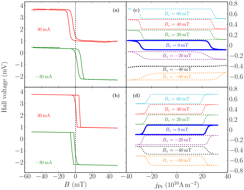
Successive current pulses with a width of are applied to the device and the Hall voltage is measured at a lower current of after each one to probe the magnetization state of the free layer. Figure 2(c-d) shows the current-induced switching of the PMA layer of two devices measured at various external applied fields . Both devices exhibit reversible SOT switching in the absence of an external field, but the loops of the two devices are opposite in sign due to opposite IEC for the two \ceRu thicknesses. We interpret this in terms of the presence of Néel domain walls in the free layer with a sign of , that is stabilised by the magnetic coupling from the pinned layer mediated via the \ceRu spacer. We also see that loops are reversed at , which corresponds to the exchange bias field of the pinned \ceCoFe. The switching of a device therefore depends on the sign of the coupling together with the value of relative to two characteristic fields of the system: the exchange bias field and the IEC field . The first is the effective field acting on the top \ceCoFe layer coming from the direct exchange with the antiferromagnetic \ceIrMn, while the second is the effective field acting on the bottom \ceCoFe layer coming from the oscillatory interlayer coupling with the top \ceCoFe via the \ceRu spacer. In the absence of external field (), is determined by the magnetization of the pinned layer and the sign of the IEC. When overcomes (), of the pinned \ceCoFe is reversed, which consequently changes the orientation of and flips the loop. For both devices, the absence of a sign reversal for ranging between zero and indicates that . Furthermore, one expects to observe the breakdown of the AFM IEC at sufficiently high external bias fields , which will again be indicated by the reversal of the loop. For , the fact that no such reversal is seen for an applied field up to gives a lower limit to . In order to test our model, we also annealed other devices with and in a magnetic field to set the exchange bias of the pinned \ceCoFe layers in opposite directions compared to devices shown here, hence exerting opposite coupling to the domain walls within the thin \ceCoFe. Those results confirm our explanation.
Finally, we used two independent methods to quantify the SOT in our heterostructures: spin Hall magnetoresistance (SMR)Chen et al. (2013); Nakayama et al. (2013); Althammer et al. (2013); Avci et al. (2015); Kim et al. and harmonic Hall measurementsKim et al. (2013); Garello et al. (2013). The measurements were performed on devices patterned from control stacks without the top pinning layers.
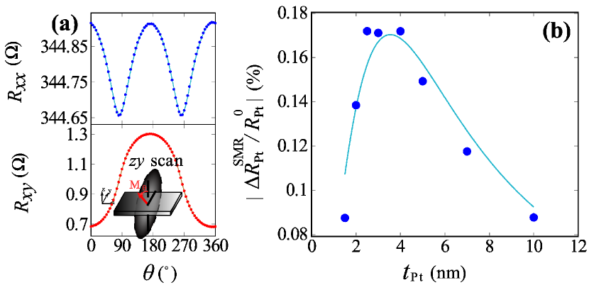
The SMR effect (Fig. 3) is caused by the simultaneous action of the spin Hall effect and the inverse spin Hall effect due to transmission and reflection of the spin current at the \cePt/\ceCoFe interface. The ratio between the reflected and the transmitted fractions of the spin accumulation depends on the relative orientation of the polarization of the electrons and the magnetic moment of the ferromagnet and on the spin-mixing conductance . If the imaginary part is negligible compared to the real part , the SOT acting on the magnetization has the form , with . We confirm by harmonic Hall measurements that this is the case for \cePtGarello et al. (2013); Emori et al. (2013). The torque is zero for , when the absorption of spin current is at a minimum and the reflection at a maximum. Hence the longitudinal resistance of the stack shows a dependence due to SMR of the \cePt/\ceCoFe bilayer.Nakayama et al. (2013); Althammer et al. (2013); Avci et al. (2015); Kim et al. In addition, the effect of the SMR is seen in the transverse resistance as an additional contribution to the planar Hall effect with an dependency on the magnetization orientation. Angular scans of and in the plane are shown in Fig. 3(a). Assuming \cePt is the unique source of SMR, it would be more appropriate to use the magnetoresistance due to SMR within the \cePt layer instead of the measured overall for rigorous SMR analysis is related to , the spin Hall angle of the system by the equationAlthammer et al. (2013); Kim et al.
| (1) |
where is the resistance of the \cePt underlayer without SMR contributions, is its resistivity and is its spin diffusion length. The values of have been determined by measuring the variation in the longitudinal resistance while rotating a external magnetic field in the plane. The best fit of the \cePt thickness dependence of with , and as parameters is shown in Figure 3(b). Using , we obtained , and , all in excellent agreement with a previous report on the \ceYIG/\cePt system.Althammer et al. (2013)
We also measured the first and second harmonic Hall responses of the same device with under a low frequency ac current excitation to quantify the effective spin-orbit fields.Kim et al. (2013); Garello et al. (2013) Considering the Hall voltage contribution from the anisotropic magnetoresistance and the SMR, we derive the longitudinal and transverse effective spin-orbit fields. As previously mentioned, the transverse field is negligible for \cePt, confirming that the imaginary part of the spin-mixing conductance and the Rashba effect are very small. We found a spin Hall angle of , in good agreement with our SMR analysis.
In summary, we have demonstrated a novel approach to achieve zero-field SOT switching using the IEC via a nonmagnetic spacer. The preferred magnetization state of the free layer with PMA is reversed upon reversing the current polarity, the exchange-bias direction or the exchange coupling sign. The coupling cannot be explained by the stray field from a flat top \ceCoFe layer, which is only antiferromagnetic and very small (), nor by the stray field created by correlated surface roughness because the Néel orange peel mechanismNéel is always ferromagnetic.
Our approach is scalable because the mechanism is independent of the area of the device as long as the dimensions are greater than the domain wall width, which is of the order of . Furthermore, SOT switching has been demonstrated down to dots with an applied field of Zhang et al. (2015), which is well within the capability of our structure.
It should be possible to develop a new three-terminal device with magnetoresistive readout by using a SOT layer which is also the spacer for magnetic coupling. An iridium spacer which exhibits high spin-orbit coupling and relatively strong IECParkin (1991) might work. Our new switching concept, which is based on well-understood phenomena and materials, takes us a step closer to the practical realisation of spin-orbit torque applications involving manipulation of perpendicular nanomagnets, which include SOT-MRAM, SOT-based magnetic logic and an SOT-based magnetic racetrack.
Methods
Sample and device fabrication
The stacks for demonstrating zero-field SOT switching are, from the substrate, \ceTa()/\cePt()/\ceCoFe()/\ceRu()/\ceCoFe()/\ceIrMn()/\cePt() (thicknesses in nanometres) and those for SMR measurements and \cePt resistivity fitting are \ceTa()/\cePt()/\ceCoFe()/\ceRu() with ranging from to . The sample from the latter series is also used for the harmonic Hall measurement and served as the reference for the switching experiment. All stacks are deposited on \ceSi(001) substrates with thermal oxide. Layers are grown by d.c. magnetron sputtering using an automated Shamrock sputtering tool with a chamber base pressure of and a growth pressure of . The growth rates of various metals are lower than , calibrated using X-ray reflectometry. The bottom \ceTa() layer serves as an adhesion layer for the \cePt, improving the PMA of the \ceCoFe. Eight-terminal Hall bar devices are fabricated using standard ultra-violet optical lithography and \ceAr ion milling. The \ceTi()/\ceCu()/\ceAu() contacts are formed by electron-beam evaporation.
Characterisation
All sample characterisation is performed at room temperature. The saturation magnetization of the thin \ceCoFe layer with PMA, obtained from the SQUID magnetometry, is , a value lower than the bulk. The angular dependence of the longitudinal and transverse magnetoresistance is measured at a d.c. current of by fixing the device in a rotating magnetic field produced by a Multimag permanent magnet variable flux source. In harmonic Hall measurements, sinusoidal a.c. excitation is generated by a WF1946B waveform generator at a frequency of and the current is measured on a series resistor using a EG&G 5210 lock-in amplifier. A small in-plane field is swept while the in-phase first harmonic and the out-of-phase second harmonic Hall signals are simultaneously detected using two SR830 lock-in amplifiers.
References
- Miron et al. (2011) I. M. Miron, K. Garello, G. Gaudin, P.-J. Zermatten, M. V. Costache, S. Auffret, S. Bandiera, B. Rodmacq, A. Schuhl, and P. Gambardella, Nature 476, 189 (2011).
- Liu et al. (2012a) L. Liu, O. J. Lee, T. J. Gudmundsen, D. C. Ralph, and R. A. Buhrman, Phys. Rev. Lett. 109, 096602 (2012a).
- Liu et al. (2012b) L. Liu, C.-F. Pai, Y. Li, H. W. Tseng, D. C. Ralph, and R. A. Buhrman, Science 336, 555 (2012b), http://www.sciencemag.org/content/336/6081/555.full.pdf .
- Fan et al. (2014) Y. Fan, P. Upadhyaya, X. Kou, M. Lang, S. Takei, Z. Wang, J. Tang, L. He, L.-T. Chang, M. Montazeri, G. Yu, W. Jiang, T. Nie, R. N. Schwartz, Y. Tserkovnyak, and K. L. Wang, Nat Mater 13, 699 (2014).
- Slonczewski (1996) J. Slonczewski, Journal of Magnetism and Magnetic Materials 159, L1 (1996).
- Berger (1996) L. Berger, Phys. Rev. B 54, 9353 (1996).
- Ikeda et al. (2010) S. Ikeda, K. Miura, H. Yamamoto, K. Mizunuma, H. D. Gan, M. Endo, S. Kanai, J. Hayakawa, F. Matsukura, and H. Ohno, Nat Mater 9, 721 (2010).
- Parkin et al. (1990) S. S. P. Parkin, N. More, and K. P. Roche, Phys. Rev. Lett. 64, 2304 (1990).
- Mangin et al. (2006) S. Mangin, D. Ravelosona, J. A. Katine, M. J. Carey, B. D. Terris, and E. E. Fullerton, Nat Mater 5, 210 (2006).
- Yu et al. (2014) G. Yu, P. Upadhyaya, Y. Fan, J. G. Alzate, W. Jiang, K. L. Wong, S. Takei, S. A. Bender, L.-T. Chang, Y. Jiang, M. Lang, J. Tang, Y. Wang, Y. Tserkovnyak, P. K. Amiri, and K. L. Wang, Nat Nano 9, 548 (2014).
- (11) L. You, O. Lee, D. Bhowmik, D. Labanowski, J. Hong, J. Bokor, and S. Salahuddin, “Switching of perpendicularly polarized nanomagnets with spin orbit torque without an external magnetic field by engineering a tilted anisotropy,” arXiv:1409.0620 .
- (12) SOT switching without external field, based on a antiferromagnet/ferromagnet bilayer has been recently reported by Fukami et al. in arXiv:1507.00888.
- Nogués and Schuller (1999) J. Nogués and I. K. Schuller, Journal of Magnetism and Magnetic Materials 192, 203 (1999).
- Parkin (1991) S. S. P. Parkin, Phys. Rev. Lett. 67, 3598 (1991).
- Dyakonov and Perel (1971) M. Dyakonov and V. Perel, Physics Letters A 35, 459 (1971).
- Hirsch (1999) J. E. Hirsch, Phys. Rev. Lett. 83, 1834 (1999).
- Brataas et al. (2000) A. Brataas, Y. V. Nazarov, and G. E. W. Bauer, Phys. Rev. Lett. 84, 2481 (2000).
- Lee et al. (2014) O. J. Lee, L. Q. Liu, C. F. Pai, Y. Li, H. W. Tseng, P. G. Gowtham, J. P. Park, D. C. Ralph, and R. A. Buhrman, Phys. Rev. B 89, 024418 (2014).
- Haazen et al. (2013) P. P. J. Haazen, E. Murè, J. H. Franken, R. Lavrijsen, H. J. M. Swagten, and B. Koopmans, Nat Mater 12, 299 (2013).
- Emori et al. (2013) S. Emori, U. Bauer, S.-M. Ahn, E. Martinez, and G. S. D. Beach, Nat Mater 12, 611 (2013).
- Torrejon et al. (2014) J. Torrejon, J. Kim, J. Sinha, S. Mitani, M. Hayashi, M. Yamanouchi, and H. Ohno, Nat Commun 5, (2014).
- Chen et al. (2013) Y.-T. Chen, S. Takahashi, H. Nakayama, M. Althammer, S. T. B. Goennenwein, E. Saitoh, and G. E. W. Bauer, Phys. Rev. B 87, 144411 (2013).
- Nakayama et al. (2013) H. Nakayama, M. Althammer, Y.-T. Chen, K. Uchida, Y. Kajiwara, D. Kikuchi, T. Ohtani, S. Geprägs, M. Opel, S. Takahashi, R. Gross, G. E. W. Bauer, S. T. B. Goennenwein, and E. Saitoh, Phys. Rev. Lett. 110, 206601 (2013).
- Althammer et al. (2013) M. Althammer, S. Meyer, H. Nakayama, M. Schreier, S. Altmannshofer, M. Weiler, H. Huebl, S. Geprägs, M. Opel, R. Gross, D. Meier, C. Klewe, T. Kuschel, J.-M. Schmalhorst, G. Reiss, L. Shen, A. Gupta, Y.-T. Chen, G. E. W. Bauer, E. Saitoh, and S. T. B. Goennenwein, Phys. Rev. B 87, 224401 (2013).
- Avci et al. (2015) C. O. Avci, K. Garello, A. Ghosh, M. Gabureac, S. F. Alvarado, and P. Gambardella, Nat Phys 11, 570 (2015).
- (26) J. Kim, P. Sheng, S. Takahashi, S. Mitani, and M. Hayashi, “Giant spin hall magnetoresistance in metallic bilayers,” arXiv:1503.08903 .
- Kim et al. (2013) J. Kim, J. Sinha, M. Hayashi, M. Yamanouchi, S. Fukami, T. Suzuki, S. Mitani, and H. Ohno, Nat Mater 12, 240 (2013).
- Garello et al. (2013) K. Garello, I. M. Miron, C. O. Avci, F. Freimuth, Y. Mokrousov, S. Blugel, S. Auffret, O. Boulle, G. Gaudin, and P. Gambardella, Nat Nano 8, 587 (2013).
- (29) L. Néel, Cr. Hebd. Acad. Sci. 255, 1676.
- Zhang et al. (2015) C. Zhang, S. Fukami, H. Sato, F. Matsukura, and H. Ohno, Applied Physics Letters 107, 012401 (2015).
Acknowledgments
This work was supported by Science Foundation Ireland through AMBER, and from grant 13/ERC/I2561. KR acknowledges financial support from the European Community’s Seventh Framework Programme IFOX, NMP3-LA-2010-246102. DB acknowledges financial support from IRCSET.
The authors thank G.Q. Yu for stimulating this work. We acknowledge G.Q. Yu, N. Thiyagarajah, and J.Y. Chen for fruitful discussions and Q. Chevigny for assistance in lithography.
Author contributions statement
Y.C.L. and D.B. contributed equally to this work. Y.C.L. and D.B. designed the experiment and planned the study with the input from K.R. D.B. grew the samples and fabricated the devices. Y.C.L. and D.B. measured the devices. D.B. performed data analysis. Y.C.L. and D.B. wrote the manuscript with advice from J.M.D.C. and P.S.
Additional information
The authors declare no competing financial interests.