Bond orbital description of the strain induced
second order optical susceptibility in silicon
Abstract
We develop a theoretical model, relying on the well established sp3 bond-orbital theory, to describe the strain-induced in tetrahedrally coordinated centrosymmetric covalent crystals, like silicon. With this approach we are able to describe every component of the tensor in terms of a linear combination of strain gradients and only two parameters and which can be estimated theoretically. The resulting formula can be applied to the simulation of the strain distribution of a practical strained silicon device, providing an extraordinary tool for optimization of its optical nonlinear effects. By doing that, we were able not only to confirm the main valid claims known about in strained silicon, but also estimate the order of magnitude of the generated in that device.
I Introduction
Silicon-based photonics has generated a strong interest in recent years, mainly for optical communications and optical interconnects in CMOS circuits. The main motivations for silicon photonics are the reduction of photonic system costs and the increase of the number of functionalities on the same integrated chip by combining photonics and electronics, along with a strong reduction of power consumption Fedeli et al. (2008). However, one of the biggest constraints of silicon as an active photonics material is its vanishing second order optical susceptibility, the so called , due to the centrosymmety of the silicon crystal. Without any second order nonlinear phenomena, fast and low power consumption optical modulation based on Pockels effect and wavelength conversions based on Second Harmonic Generation (SHG) are not possible in bulk Si Leuthold et al. (2010). This is a very limiting factor when we expect silicon to be part of a solution to high performances and high energy efficient devices Reed et al. (2010).
To overcome this problem, strain has been used as a way to deform the crystal and destroy the centrosymmetry which inhibits . In fact, over the last few years Pockels electro-optic modulation Jacobsen et al. (2006); Chmielak et al. (2011, 2013); Puckett et al. (2014); Damas et al. (2014) and SHG Cazzanelli et al. (2012); Schriever et al. (2012) have been claimed to be demonstrated in devices where the silicon active region is strained by a stress overlayer, usually made of SiN. Motivated by its enormous potential, the interest in strained silicon photonics devices has been growing in the past years. However, there is a lack of fundamental understanding on the process through which the strain tensor generates non vanishing tensor components. In other words, there is no available general quantitative relationship between these two quantities.
Despite the different attempts to find a solution to this problem, no theoretical model showing a practical relationship between the components of the second order nonlinear optical susceptibility and the strain tensor has been published yet. Such model is fundamental in the field of strained silicon photonics because it permits a connection between the strain effects, easy to simulate with the right computational tools, and the respective induced nonlinear phenomena. Without this knowledge, it is not possible to design and optimize structures based on strained silicon structures for the maximum outcome of effects.
The first proposed models connecting with Govorkov et al. (1989); Huang (1994) were based on the deformation potentials in semiconductors. The deformation potentials theory relies on the de-localisation of the Bloch wavefunction over the entire crystal and proves to be a good description for the study of transport properties of electrons. However, it is known now that the nonlinear optical properties in covalent crystals are mainly due to the properties of the localized electrons in the covalent bonds between the different atoms of the crystal Levine (1973, 1969); Kleinman (1962); Harrison and Ciraci (1974); Aspnes (2010). Thus, theories based on the deformation potentials not only prove to be very limiting for extracting the different components in terms of , but also do not show a very good numerical agreement with the experimental data for in strained silicon Govorkov et al. (1989); Hon et al. (2009a).
Later, simpler models based on Coulomb interactions between atoms were also suggested Hon et al. (2009b, a), but none of them proved to a good description of the phenomena, both numerically and conceptually. To overcome this difficulty, ab-initio calculations were performed as an attempt to understand how the change in position of the atoms enables in the crystal Cazzanelli et al. (2012); Luppi et al. (2015). Although they proved to be an accurate description of the problem, they are very computationally demanding and do not provide a practical, quantitative and spatial relationship between and the strain in the crystal and thus do not allow for device design over the strain distribution.
Even though the underlying process has not been described yet, it has been widely claimed that there is a direct relationship between and the strain gradients inside silicon Cazzanelli et al. (2012); Chmielak et al. (2013); Puckett et al. (2014); Damas et al. (2014); Schriever et al. (2015). In fact, very recently Manganelli et al. Manganelli et al. (2015) proposed a model based on symmetry arguments to show a linear relationship between both the spatial distribution of and tensor components. However, even though the theory is well developed, it is very dependent on parameters required to be determined experimentally. This poses a problem because very recently it has been shown that the reported electro-optic measurements of strained silicon devices have a strong contribution from free carriers effects inside the silicon waveguide Azadeh et al. (2015); Sharma et al. (2015); Schriever et al. (2015). Therefore, most of the available numerical data of strain induced in silicon waveguides available in the literature was misinterpreted and discredited, making it impossible at the moment to find the experimental parameters predicted by the model presented in Manganelli et al. (2015).
Although many works have been reported, no consistent study based on the bond orbital model has been reported yet on the study of the strain induced nonlinear effects in Si. The bond orbital model is the most widely accepted model to describe the properties of electrons in the bonds of a tetraheral covalent crystals like silicon Harrison (1989, 1973a); Harrison and Ciraci (1974). Relying on the well established quantum mechanics of the sp3 hybridization of silicon valence electrons, the bonding electrons are treated quantum-mechanically to describe their properties. This procedure has already been used to characterize the strain effects Harrison and Phillips (1974) and nonlinear optical properties Harrison (1989) in covalent crystals, although treated separately.
In the present work, we rely on the original work first developed by Harrison et al. in Harrison (1973a) to describe the bonding electrons. By using the bond orbital model and keeping only first order effects in strain and strain gradients, we are able to show a practical way of knowing any component generated by the strain ( ) in that point in space. The results not only show very good agreement with the main claims made in the literature about the relationship between and strain in silicon, but also depends only on 2 parameters which can be predicted theoretically and depend only on the material.
The organization of this paper is as follows: we start by presenting the general reasoning behind the model before entering into the quantum mechanical treatment of the sp3 hybridization in strained covalent crystals, in part II.1. In section II.2 we proceed to the calculation of the strain induced polarity of a covalent bond and in section II.3, we deduce its second order nonlinear dipole moment. This will allow us to extract the strain induced components in terms of the strain tensor ( ) components. Finally, in section III we apply our model to a particular example device, showing the degree of the agreement and its practical applicability.
II The strain induced in covalent crystals
Silicon is a tetrahedral covalent crystal, where two neighbour atoms are bond together by sharing electrons, creating a covalent bond Harrison (1989). Four covalent bonds organize themselves in a tetrahedral configuration as shown in Fig.1. Understanding any property of the crystal (like ) requires studying the quantum mechanical interactions of the electrons in the bonds. However, to make it clearer for the reader, before entering in any mathematical description, we start by presenting the process suggested in this work for the generation of in each bond due to the strain.
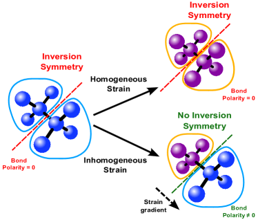
It is known that depends primarily on the polarity of the bonds of a crystal Harrison and Ciraci (1974); Levine (1973, 1969). The polarity of a bond is the difference of energy of the two electrons making the bond. In a centrosymmetric crystal, since the electrons feel the same energy in both directions, the bonds are unpolar, as shown in Fig. 1. However, when strain is applied to a crystal, the atomic configuration changes and a bond becomes polar if and only if there is a strain gradient in the direction of the bond. This process is presented schematically in Fig. 1, where the blue and yellow contours represent different values of energy. This explains why inhomogeneous strain fields are required to induce bond polarity and thus , because homogeneous strain changes the electronic energy in the same way in both electrons of the bond.
This is the idea behind the mathematical and quantum description of the problem: first we calculate how the strain changes the polarity of a bond and from then we deduce how that strain induces second order nonlinear effects. Moreover, even though in this work we focus on silicon atoms, this procedure can be applied to any covalent diamond crystal structure.
II.1 Quantum mechanical treatment of a strained covalent crystal
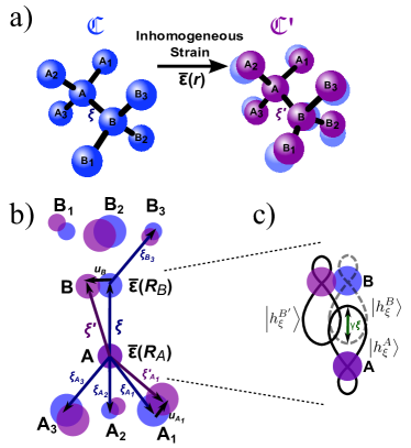
Consider a tetrahedral covalent crystal , represented in blue in the 3D scheme of Fig. 2 a). The four valence electrons in a general Si atom organize themselves in four different sp3 hybrids pointing in the direction of the four nearest neighbours, creating four bonds . Such hybrid orbitals on any given atom are orthogonal to each other if the near neighbours are exactly tetrahedral, like in an unstrained Si crystal Harrison (1973a).
Consider now the lattice (represented in purple), the strained version of . Each atom in is slightly moved by a vector in relation to and the new atomic organization in will change a bond into (see Fig. 2 b) ). To study this new bonding, it may sound appealing to construct four new hybrids out of the atomic orbitals, with the direction . However, since the atoms are not arranged in a tetrahedral configuration anymore, such set of hybrids would not be orthogonal and it would require a special treatment afterwards Harrison (1973b). To overcome this problem, we will construct the wavefunction of the electrons in any atom has a combination of the original hybrids , placed in the new atomic positions. This is schematically represented in the Fig. 2 c), making it possible to deal with the quantum mechanical subtleties of this problem, as it will be apparent later on.
Consider now, without any loss of generality, atom , taken as the atom which preserves the same position in and , as shown in Fig. 2 a) and b). This atom is connected to four other atoms. We focus on one of its four bonds, connecting atom with atom and call it bond . The bond vector (associated with bond ) is defined as the vector from atom to atom . (Fig. 2 b) ).
To study the quantum mechanical properties of the electrons in the bond, we must start by building its Hamiltonian. The one-electron Hamiltonian of the strained crystal lattice is given by Huang (1975):
| (1) |
where is the kinetic energy of the electron and is the potential due to the atom in position . This potential can be written as
| (2) |
with being the contribution from the strain effects, vanishing for an unstrained crystal. We have explicitly separated and from the sum in eq. 1 because we are focusing on the bond between atoms and and its treatment is more clear this way.
The matrix element of in is given by
| (3) |
being equivalent in . We should now try to relate them to the same matrix elements of the unstrained Hamiltonian in the original hybrids basis. Since the hybrid wavefunctions and are respectively centred at the atoms and in , we have:
| (4) | |||||
| (5) |
Moreover, because of the symmetry of the bond, the potential of in is the same as the potential of in . Thus,
| (6) |
where and is the correction accounting for the new relative position of atoms and in .
For all the other atoms (), we can write:
| (7) | |||||
| (8) | |||||
From the previous analysis and after eq. 3, we are in conditions of writing the matrix elements of as
The terms and are the average energy of and in and because of its centrosymmetry, they have both the same value .
In addition, the effects of strain on the cross term has been studied by Harrison et al. in Harrison and Phillips (1974) and it is shown that
where and a fitting constant. This shows that the Hamiltonian cross term has a second order correction in the strain effects.
The obtained Hamiltonian matrix elements will be used now to calculate the polarity of the bond in the strained crystal.
II.2 Strain induced bond polarity
The polar energy (or polarity) of the bond in the strained crystal is defined by (Harrison, 1973a; Harrison and Ciraci, 1974)
| (9) | |||||
| (10) |
and it can be immediately seen that if , i.e. no strain is applied to the crystal, and the bonds are non-polar. This is the reason behind the vanishing in non-strained centrosymmetric crystals.
By reducing the sum in equation 10 only to the interaction between the first neighbours of atoms and individually, and respectively as shown in Fig. 2 a) and b), equation 10 reduces to
| (11) |
Despite we have not said anything about the form of the crystal potential yet, we know it is a central potential () and for big enough, it should behave like a Coulomb potential. Therefore, for small displacements of the atoms, we may assume that and the form of defined in equation 2 can be taken by performing a first order Taylor expansion of the potential :
By defining , it is clear that
| (12) |
which can only be evaluated once we know the explicit form of .
Using this definition along with the symmetries of the bond, the central properties of the potential and bearing in mind that the hybrid wavefunctions statisfy , it can be shown that
leading to the simplification of equation 11 into
| (13) |
Assume now that there is a known strain field in the crystal as shown in Fig. 2 b) and that the strain applied to each atom is given by . From simulations of the strain distribution in a Si crystal, it can be shown that the strain is a slowly varying function over the bond length (). In that case, by defining as the bond vector between atoms and and respectively for B (Fig. 2 b) ), it is easy to show using elasticity theory that Landau and Lifshitz (ress); Bir and Pieu (1972)
| (14) | |||||
| (15) |
Since the strain changes slowly in distances of the bond length , we can relate the component of the strain tensor in atoms and by making a first order Taylor expansion
which allows us to write the final expression of the polarity of a bond in atom as
| (16) |
where we have defined the rank-2 tensor (related to the bond in the atom located in the position ), whose component is given by
| (17) |
Furthermore, the vector is defined by
| (18) | |||||
| (19) | |||||
| (20) |
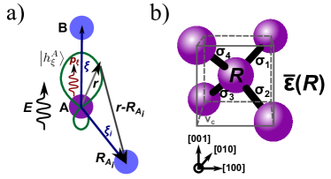
Its evaluation can be done with the help of the scheme in in Fig. 3 a). It does not depend on the atom in particular, but only on the unstrained bonds , which are the bonds different than in the unit cell (compare Fig. 3 a) with Fig. 2 b)).
The closed form of can only be found once the potential is known. However, regardless of that, we can always define
| (21) |
where and are parameters whose values are related to the projections of on and respectively and are characteristic of the crystal material in consideration. This definition together with equation 16, allows us to write
| (22) |
Expression 22 is the final expression for the polar energy (or polarity) of any bond in an atom centred in the unit cell located in (see Fig. 3 b) ). The subscript identifies one of the four bonds, which defines the corresponding bond vector and then the 3 other vectors . We see that it depends on the strain gradients through , which is non-zero only if there is a strain gradient component in the direction of the bond . This is relevant because it shows that in a centro-symmetric crystal not only a strain gradient is required to create a polar bond, but it also gives the preferred gradient direction to obtain maximum polarity in bond .
Moreover, once the strain distribution is known, the only parameters left to know are and . These two coefficients are the only unknowns of the model presented so far and their value (defined in equation 21) should be found experimentally, but this particular point requires further attention and it will be discussed later in section III.1.
II.3 The second order nonlinear optical dipole moment
Now that the polarity of a strained bond is known in terms of the strain tensor , we can explore the nonlinear optical properties of the bond by computing the bond wavefunction and extract the second order dipole moment of the electrons in that bond. We now approach the problem as in the original theory done by Harrison et al in Harrison and Ciraci (1974). The bond wavefunction of the bond is considered to be a combination of the two adjacent hybrids of the atoms forming that bond (Fig. 2 c) ) Harrison (1973b); Harrison and Ciraci (1974); Harrison (1973a)
| (23) |
and is obtained by minimizing the bond energy . In doing so, we are implicitly neglecting all the matrix elements of the Hamiltonian and all other hybrid overlaps are neglected (or absorbed in the parameters we have retained). It is important to bear in mind that . Under these conditions, the explicit values for and can be found in the original work presented in Harrison and Ciraci (1974).
The average position of the bond wavefunction in a strained crystal, in relation to the center of the bond, can be shown to be given by Harrison and Ciraci (1974)
| (24) |
which reduces to in a non-strained crystal, the same result presented in Harrison and Ciraci (1974). In its original work, Harrison Harrison and Ciraci (1974) introduces the parameter which accounts for the distance between the ”center of gravity” of each hybrid as shown in Fig. 2 c) and it would be unity if they were centred at the nucleus.
When an optical electric field interacts with the bond, it will induce a dipole moment , as represented in red in Fig. 3 a). That dipole moment will change the Hamiltonian by a term , which will change the bond wavefunction , yielding new coefficients and . Finally, the dipole moment in the bond, created by the optical field will be given by which will depend on the intensity of the optical electric field . By expanding in powers of , the second order term is shown to be given by Harrison and Ciraci (1974); Harrison (1989)
| (25) |
The previous expression is drastically simplified if we stick only to first order terms in strain effects, i.e. in and . Since defined in 22 is directly proportional to the strain gradients, keeping the terms proportional to in eq. 25 means retaining terms of the form , i.e. of second order in strain effects. Therefore, we must remove all terms from eq. 25 to keep everything to first order in strain effects. Moreover, is nothing more than half of the bandgap of the crystal Harrison and Ciraci (1974); Jha and Bloembergen (1968); Harrison (1989); Huang (1994); Phillips (1968) which is much bigger than the strained induced polarity of the bond, . All these considerations finally lead to:
| (26) |
Expression 26 is the final second order nonlinear dipole moment to first order in the strain effects. It can be seen the direct relationship between and , which justifies why nonpolar bonds do not contribute to 2nd order nonlinear effects. Also, it is worth to stress the fact that the strain effects in are all inside : everything else, including the bond vector , is related to the unstrained crystal lattice. This is relevant because it shows that to first order in the strain effects, only the strain gradients are important to the polarity of the bonds and thus to generation.
The macroscopic 2nd order nonlinear polarization is the sum of the contributions of the 4 bonds in the crystal unit cell centred in , divided by its volume (Fig. 3 b) ). Thus
| (27) | |||||
| with |
Using the corresponding values for Si, taking Harrison (1989) and Harrison and Ciraci (1974), we have C3m-3eV-3.
For a bond length , the bond vectors in the crystal coordinates are given by
| , | (28) | ||||
| , | (29) |
and replacing these coordinates in equation 27, we can write the final components of the 2nd order nonlinear polarization in the crystal coordinates as
| (30) | |||||
| (31) | |||||
| (32) | |||||
The previous set of equations, together with the definition
| (33) |
determines every and each component of the tensor in the crystal coordinates in terms of the polarity of each bond in the unit cell, as represented in Fig. 3 b). This polarity, depends on the sum of the strain gradients projected on the direction of each bond, as shown by equation 17, leading to a different polarity of each bond in the unit cell. Therefore, in general, every component of will be non-zero, contrasting with the case of a zync-blend crystal where each bond has the same polarity and in which case equations 30, 31 and 32 lead to the well known fact that is the only nonvanishing component.
The explicit calculation of the components in terms of the strain gradients, requires an explicit expansion of the sum defining in equation 22. Despite being always possible to do it in terms of the unknown parameters and , we will not write it explicitly for a general case, not only because it turns out to be a very big expression, but also it depends on the lab coordinate system relevant for that particular situation. Therefore, we will apply the previous formulations of in strained silicon to a relevant device where we can actually analyse how the strain enables its effects.
III Evaluation of the proposed model
To fully validate the model presented in the previous sections, an experimental confirmation would be required. However, as already briefly mentioned in the introduction, very recently it has been shown that the experimental data available in the literature on phenomena in strained silicon, has a strong contribution from free carriers effectsAzadeh et al. (2015); Sharma et al. (2015); Schriever et al. (2015). This parasitic response masks the real value of strain induced in silicon, resulting in erroneous experimental data.
As a result, most of the quantitative values of in strained silicon presented in the literature Chmielak et al. (2011, 2013); Damas et al. (2014); Puckett et al. (2014) have been discredited and no reliable data is available to confidently compare with the results from our model. Nevertheless, there are some properties of strain-induced in silicon that are sill known to be valid and we will apply our model to a practical device and take conclusions regarding those characteristics.
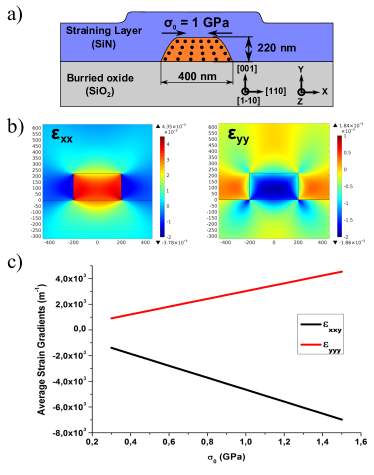
We will evaluate the validity of our theory by applying it to the waveguide structure shown in Fig. 4 a), which is the structure usually used in strained silicon devices towards Pockels effect modulation Chmielak et al. (2011, 2013); Damas et al. (2014). The waveguide coordinates are then given in terms of the crystal coordinates by
The straining layer placed on top of the waveguide has an initial stress , which will induce a strain field in the waveguide. Since the waveguide extends over the direction, the strain/strain gradients components can be neglected. In addition, our simulations show that the cross strain components inside the Si waveguide are much smaller than the principal ones , so we will neglect their contribution in our analysis. Therefore, by defining the strain gradient components by
we are only left with the components , , and .
The strain induced bond polarities (eq. 22) in the waveguide coordinates, are calculated after rewriting the bond vector coordinates (Eq. 28) in the lab basis. The components in the lab coordinates can be extracted after replacing the polarities into equations 30, 31 and 32 for the macroscopic polarization, in the lab coordinates. After these calculations are performed, the relevant components for this device become:
| (34) | |||||
| (35) | |||||
| (36) | |||||
| (37) |
This set of equations gives us all the required information about the tensor in any point of space in terms of the strain gradients in that same point. We can now compare this result with the main claims on strain-induced in silicon.
We start by noticing that the previous equations have the form
| (38) |
which is a linear combination of strain gradients, as previously suggested in Manganelli et al. (2015); Damas et al. (2013). Moreover, from our model the coefficients are known and depend only on and . For instance, from equation 36 we extract
| (39) |
and this can be done to any coefficient , always in terms of only and . This is in line with the claims that should be proportional to strain gradients and not to strain itself, as it has been suggested in many publications in the past years Cazzanelli et al. (2012); Chmielak et al. (2013); Puckett et al. (2014); Damas et al. (2014); Manganelli et al. (2015); more importantly it gives the exact value of the weight of each strain gradient direction for the desired component.
Other known experimental fact of strained silicon is that has a linear relationship with the initial stress in the straining layer Huang (1994); Schriever et al. (2010, 2012).
In Fig. 4 c), we see the simulation of the average and in the waveguide, for different values of and it is clear the linear relationship between these 2 quantities. This is true for any component. Since is linear with , it is straightforward to conclude that, regardless of the values of and , our model predicts
| (40) |
which is coherent with the experimental data in Schriever et al. (2010).
III.1 Estimation of the order of magnitude of
As it can be seen from eqs. 34 - 37, depends entirely on the parameters and , defined in Eq. 21. To determine these two parameters, the best approach would be to fit the experimental data to the proposed model and extract the values of and that give the best fit.
However, as already mentioned, all the quantitative values of strain induced in silicon published in the literature, in particular those in Chmielak et al. (2011, 2013); Puckett et al. (2014); Damas et al. (2014) have strong parasitic contributions from carriers Azadeh et al. (2015); Sharma et al. (2015); Schriever et al. (2015). Therefore, no reliable numerical data for in strained silicon is available right now to allow for a confident fitting of or and their evaluation must be done by approaching the definition in eq. 21.
The evaluation of the integral in eq. 18 is not a simple task, not only because it is a difficult integral to evaluate, but mainly because the real form of the silicon crystal potential must be entirely known. The potential is recognized to be difficult to know exactly Witzens (2014), so any result deduced from will always have associated errors. Newertheless, the order of magnitude of the predicted values, must present a considerable level of agreement with the most recent experimental results on strained silicon. Therefore, we will focus on determining the order of magnitude of in eqs. 34-37.
In order to evaluate the order of magnitude of , we must simplify the integral in eq. 18. To do that, we will make the approximation , which basically means that the hybrid wavefunction is considered to be strong only close to the original atom. Despite this is not entirely true because it extends along its bond, this simplification should not change considerably the order of magnitude of the integral of eq. 18. In that case, eq. 20 becomes
| (41) | |||||
| (42) |
The previous equation gives us values for and which are merely approximations, but should be in the same order of magnitude of the real ones:
| (43) |
As already mentioned, the determination of the real Si crystal potential is a very complex problem, which has been studied for many years Appelbaum and Hamann (1973); Anderson (1969); Chelikowsky et al. (1991); Wendel and Martin (1978). Because of its complexity, in this work we will only compare two simple crystal potentials to extract some numerical information: the Coulomb potential generated by a Si4+ ion
| (44) |
and the Phillips potential for Si Phillips and Kleinman (1959)
| (45) |
with kg m3/s2 and the parameters , and m-1.
Using eq. 43 for both of these potentials, taking nm and focusing only the component (which is the one that has been more strongly studied in the literature Jacobsen et al. (2006); Chmielak et al. (2011, 2013); Puckett et al. (2014); Damas et al. (2014)), we get for the Coulomb and Phillips potentials, respectively (in S.I. units):
| (46) | |||||
| (47) |
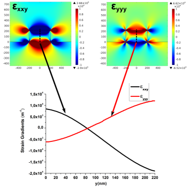
Now, as shown in Fig. 5, the typical order of magnitude of the strain gradients on the edges of the waveguide (where the applied electric field is stronger Sharma et al. (2015)) is , leading to:
| (48) |
The strong dependence of on the choice of potential is clear from the results above. It means that any difference between predicted and experimental results can be attributed to a bad choice of the potential used to describe the crystal. This problem can only be overcome by fitting and to available experimental data. Any other way of obtaining these two parameters, will inevitably have errors associated because the used potential will always be an approximation to the real and much more complex potential felt by the electrons in a real crystal.
On the other hand, it is not straightforward which published experimental values we should compare to. It is now widely accepted that previously reported values of on the order of magnitude of pm/V as the ones published in Chmielak et al. (2011, 2013); Damas et al. (2014) were wrongly interpreted and they are mainly due to free carriers effects and not to strain. In fact, latest results, which account for carriers effects, suggest values of much lower than these and their order of magnitude should be around pm/V Schriever et al. (2015) or even as low as pm/V Borghi et al. (2015). Moreover, even these lower values of could have been erroneously estimated as latest publications suggest that the electric field applied to the waveguide to induce Pockels effect modulation (the method used to experimentally obtain these values) is not homogeneous through the waveguide, but strongly modified by carriers effects Sharma et al. (2015), which does not seem to have been taken into account in these publications.
Nevertheless, we see that the values presented by our model in equation 48, even though we used very simplified potentials , are very close, in order of magnitude, to the latest experimental results available on strain induced .
IV Conclusion
In this work we develop and present an atomistic model, based on the bond orbital model to describe the second order nonlinear effects generated by strain in the silicon crystal. This model gives a spatial quantitative and well defined relation between the tensor and the strain tensor .
We have shown that is proportional to a weigthed sum of strain gradient components, as suggested by many publications. The weighting coefficients depend only on 2 coefficients, and , which can be theoretically estimated, but should be experimentally determined to fully validate this model.
By applying this model to a specific geometry, with the characteristics of the main devices used in strained silicon photonics for Pockels effect modulation, we were able to show agreement of our model with the known properties of strain induced in silicon. Furthermore, we estimated the order of magnitude of a component of calculated using our model and its values (between 1 pm/V and 8 pm/V) showed a considerable agreement with the latest published experimental results. Nevertheless, this value can be strongly improved once reliable experimental data is available for a confident fit of the numerical predictions of this model.
We consider that the presented model is of extreme relevance for the study of nonlinear effects in strained silicon photonics. With the relation between and that we developed in this paper, the optimization of strained silicon devices is finally possible. The strain distribution in the crystal can be engineered to maximize the most relevant components for the desired device and this opens a whole new route towards the improvement of nonlinear effects in strained silicon, bringing us closer to high performance devices based on this kind of effects.
Acknowledgements.
Authors would like to thank Xavier Le Roux from IEF and Frédéric Boeuf from STMicroelectronics (Crolles, France) for fruitful discussions. The authors also acknowledge STMicroelectronics for the financial support of the P. Damas’ scholarship. This project has received funding from the European Research Council (ERC) under the European Union’s Horizon 2020 research and innovation program (ERC POPSTAR - grant agreement No 647342).References
- Fedeli et al. (2008) J. M. Fedeli, L. D. Cioccio, D. Marris-Morini, L. Vivien, R. Orobtchouk, P. Rojo-Romeo, C. Seassal, and F. Mandorlo, Adv. Optical Technol., Special issue on ”Silicon Photonics” (2008).
- Leuthold et al. (2010) J. Leuthold, C. Koos, and W. Freude, Nature Photonics 4, 535 (2010).
- Reed et al. (2010) G. T. Reed, G. Mashanovich, F. Y. Gardes, and D. J. Thomson, Nature Photonics 4, 518 (2010).
- Jacobsen et al. (2006) R. S. Jacobsen, K. N. Andersen, P. I. Borel, J. Fage-Pedersen, L. H. Frandsen, O. Hansen, M. Kristensen, A. V. Lavrinenko, G. Moulin, H. Ou, C. Peucheret, B. Zsigri, and A. Bjarklev, Nature 441, 199 (2006).
- Chmielak et al. (2011) B. Chmielak, M. Waldow, C. Matheisen, C. Ripperda, J. Bolten, T. Wahlbrink, M. Nagel, F. Merget, and H. Kurz, Optics express 19, 17212 (2011).
- Chmielak et al. (2013) B. Chmielak, C. Matheisen, C. Ripperda, J. Bolten, T. Wahlbrink, M. Waldow, and H. Kurz, Optics Express 21, 25324 (2013).
- Puckett et al. (2014) M. W. Puckett, J. S. T. Smalley, M. Abashin, A. Grieco, and Y. Fainman, Optics letters 39, 1693 (2014).
- Damas et al. (2014) P. Damas, X. Le Roux, D. Le Bourdais, E. Cassan, D. Marris-Morini, N. Izard, T. Maroutian, P. Lecoeur, and L. Vivien, Optics Express 22, 22095 (2014).
- Cazzanelli et al. (2012) M. Cazzanelli, F. Bianco, E. Borga, G. Pucker, M. Ghulinyan, E. Degoli, E. Luppi, V. Véniard, S. Ossicini, D. Modotto, S. Wabnitz, R. Pierobon, and L. Pavesi, Nature materials 11, 148 (2012).
- Schriever et al. (2012) C. Schriever, C. Bohley, J. Schilling, and R. B. Wehrspohn, Materials 5, 889 (2012).
- Govorkov et al. (1989) S. V. Govorkov, V. I. Emel’yanov, N. I. Koroteev, G. I. Petrov, I. L. Shumay, V. V. Yakovlev, and R. V. Khokhlov, Journal of the Optical Society of America B 6, 1117 (1989).
- Huang (1994) J. Huang, Jpn. J. Appi. Phys. Vol 33, 3878 (1994).
- Levine (1973) B. Levine, Physical Review B 7, 2600 (1973).
- Levine (1969) B. Levine, Physical Review Letters 22, 787 (1969).
- Kleinman (1962) D. Kleinman, Physical Review 126, 1977 (1962).
- Harrison and Ciraci (1974) W. Harrison and S. Ciraci, Physical Review B 10 (1974).
- Aspnes (2010) D. E. Aspnes, Physica Status Solidi (B) 247, 1873 (2010).
- Hon et al. (2009a) N. N. K. Hon, K. K. K. Tsia, D. R. D. Solli, B. Jalali, and J. B. Khurgin, in 2009 6th IEEE International Conference on Group IV Photonics (IEEE, 2009) pp. 232–234.
- Hon et al. (2009b) N. K. Hon, K. K. Tsia, D. R. Solli, and B. Jalali, Applied Physics Letters 94, 091116 (2009b).
- Luppi et al. (2015) E. Luppi, E. Degoli, M. Bertocchi, S. Ossicini, and V. Véniard, Physical Review B 92, 075204 (2015).
- Schriever et al. (2015) C. Schriever, F. Bianco, M. Cazzanelli, M. Ghulinyan, C. Eisenschmidt, J. de Boor, A. Schmid, J. Heitmann, L. Pavesi, and J. Schilling, Advanced Optical Materials 3, 129 (2015).
- Manganelli et al. (2015) C. L. Manganelli, P. Pintus, and C. Bonati, Opt. Express 23, 28649 (2015).
- Azadeh et al. (2015) S. S. Azadeh, F. Merget, M. P. Nezhad, and J. Witzens, Optics letters 40, 1877 (2015).
- Sharma et al. (2015) R. Sharma, M. W. Puckett, H.-H. Lin, F. Vallini, and Y. Fainman, Applied Physics Letters 106, 241104 (2015).
- Harrison (1989) W. A. Harrison, Electronic Structure and the Properties of Solids, Dover Books on Physics (Dover Publications, 1989).
- Harrison (1973a) W. Harrison, Physical Review B 8 (1973a).
- Harrison and Phillips (1974) W. Harrison and J. Phillips, Physical Review Letters 33, 6 (1974).
- Harrison (1973b) W. Harrison, Physical Review A 7, 1876 (1973b).
- Huang (1975) C. Huang, (1975).
- Landau and Lifshitz (ress) L. D. Landau and E. M. Lifshitz, The Theory of Elasticity, Vol. 7 (required, Pergamon Press).
- Bir and Pieu (1972) G. L. Bir and G. E. Pieu, Symmetry and Strain-Induced Effects in Semiconductors (John Willey and Sons, New York/Toronto, 1972).
- Jha and Bloembergen (1968) S. Jha and N. Bloembergen, Physical Review 171 (1968).
- Phillips (1968) J. Phillips, Physical Review 168, 905 (1968).
- Damas et al. (2013) P. Damas, X. L. Roux, E. Cassan, D. Marris-morini, N. Izard, A. Bosseboeuf, T. Maroutian, P. Lecoeur, and L. Vivien (2013) pp. 11–13.
- Schriever et al. (2010) C. Schriever, C. Bohley, and R. B. Wehrspohn, Optics letters 35, 273 (2010).
- Witzens (2014) J. Witzens, Computer Physics Communications 185, 2221 (2014).
- Appelbaum and Hamann (1973) J. a. Appelbaum and D. R. Hamann, Physical Review B 8, 1777 (1973).
- Anderson (1969) P. W. Anderson, Physical Review 181, 25 (1969).
- Chelikowsky et al. (1991) J. R. Chelikowsky, K. M. Glassford, and J. C. Phillips, Physical Review B 44, 1538 (1991).
- Wendel and Martin (1978) H. Wendel and R. M. Martin, Physical Review Letters 40, 950 (1978).
- Phillips and Kleinman (1959) J. C. Phillips and L. Kleinman, Physical Review 116, 287 (1959).
- Borghi et al. (2015) M. Borghi, M. Mancinelli, F. Merget, J. Witzens, M. Bernard, M. Ghulinyan, G. Pucker, and L. Pavesi, Opt. Lett. 40, 5287 (2015).