Dirac electrons on three-dimensional
graphitic zeolites
— a scalable mass gap
Abstract
A class of graphene wound into three-dimensional periodic curved surfaces (“graphitic zeolites”) is proposed and their electronic structures are obtained to explore how the massless Dirac fermions behave on periodic surfaces. We find in the tight-binding model that the low-energy band structure around the charge neutrality point is dominated by the topology (cubic or gyroid) of the periodic surface as well as by the spatial period in modulo 3 in units of the lattice constant. In both of cubic and gyroid cases the Dirac electrons become massive around the charge neutrality point, where the band gap is shown to scale as within each mod-3 class. Wave functions around the gap are found to have amplitudes sharply peaked around the topological defects that are required to deform the graphene sheet into a three-dimensional periodic surface, and this is shown to originate from non-trivial Bloch phases at and points of the original graphene.
pacs:
73.22.Pr, 73.61.-r, 03.65.PmIntroduction— While a vast variety of phenomena arising from massless Dirac electrons have been revealed for two-dimensional (2D) graphene, a natural and important question is what will happen to the electronic structure if three-dimensional (3D) structures are constructed from graphene. Specifically, when we envisage structures that are periodic in each of and directions, we are talking about triply-periodic surface, or “graphitic zeolites”, where we have a 3D network of graphene sheets. Interests are, first, band-theoretically how the massless Dirac particles behave in totally different spatial topologieshelicoid1 . Second, when the flat honeycomb lattice of graphene is wound into such 3D geometries, we have to introduce topological defects, and the electronic properties of carbon systems in such cases have been studied in the context of fullerenes, carbon nanotube caps and graphene cones.Kroto85 ; Iijima91 ; Gonzalez92 ; Gonzalez93 ; Tamura94 ; Tamura97 ; Lammert04 For a 3D graphitic zeolite, we have to introduce topological defects as more than six-membered rings, around which the surface has negative Gaussian curvatures,Terrones91 ; Terrones92 ; Vanderbilt92 ; Lenosky92 as illustrated in Fig. 1.
Thus the question we pose here is: In such 3D graphene structures, how its low-energy spectrum would look like — can it still be a 3D massless Dirac electron, or otherwise, especially around the “charge neutrality point” (originally the Dirac point of flat graphene)? The question is not only academic, but should be relevant to the electronic properties in 3D carbon nanostructures that are realized in recent experiments.Ma2001 ; Ma2002 ; kyotani2009 ; Li2013 ; Wu2013 ; Xu2013 ; WChen2011 ; Yang2013 ; ZChen2011 ; Cao2011 ; Ito2014 Specifically, a high-quality 3D graphene network was very recently fabricated with a nanoporous template material,Ito2014 where the system was found to comprise interconnected single graphene sheet with structural length scale of 100 nm to 1 m. While the samples fabricated are not periodic, they are expected to retain the low-energy characteristics of graphene owing to a high quality, so that they should serve as a starting point for realizing massless Dirac particles on curved surfaces.
Theoretically, band structures of periodic curved surfaces have been studied for conventional (nonrelativistic) electrons for various surfaces including Schwarz’s P (simple cubic) and D (diamond-structured) surfacesAoki2002 ; Aoki2004 and also G (gyroid) surface.KoshinoAoki2005 The massless Dirac particle on periodic curved surfaces poses an entirely different problem. A crucial interest is the fate of the Dirac cone in the band structure in these structures. Possible structures of 3D periodic graphene were first theoretically proposed Terrones91 ; Terrones92 ; Vanderbilt92 ; Lenosky92 ; Fujita95 ; Weng2014 ; Tagami2014 , and band structures were obtained for some specific cases with relatively small unit-cell sizes of the order of the atomic scale. However, to consider systematics of the Dirac particle on periodic curved surfaces on a more general ground, particularly around the charge neutrality point, we need to look at the energy band structure not only for 3D structures with different topologies, but for different length scales in the periodic structures to fathom the scaling behavior of the band structure and mass gap.
These have motivated us to study in this paper the electronic energy spectra of 3D graphene networks with varied spatial periods and structures. As the surface topology, we consider two typical periodic minimal surfaces, which are called Schwarz’s P-surface (cubic) and G-surface (gyroid with helical symmetry along each of directions) as shown in Fig. 1(a) and (b), respectively. We construct the corresponding honeycomb networks having these topologies as illustrated in Fig. 2, and calculate the band structure with the simple tight-binding model. By varying the periodicity of these 3D structures we study the scaling behavior of the band structure around the charge neutrality point.
We shall first find that the energy spectrum around the charge neutrality point is essentially determined by the surface topology (P or G). In each case we reveal a “mod-3 rule”, where the spatial period in modulo 3 in units of the original honeycomb lattice constant dominates the bands. The systems in the same category (with the same topology and the same mod-3 number) have almost identical low-energy band structures, where energy (band width, etc) scales as , where is the spatial period. In each case, the original Dirac cone becomes massive with the mass gap also scaling as . Thus we conclude that massless Dirac electron bound on the 3D periodic surfaces behaves as a massive Dirac electrons with a scalable mass. We also find the wave functions around the gap have singularily large amplitudes concentrated around the topological defects that are required to make the system periodic in 3D.
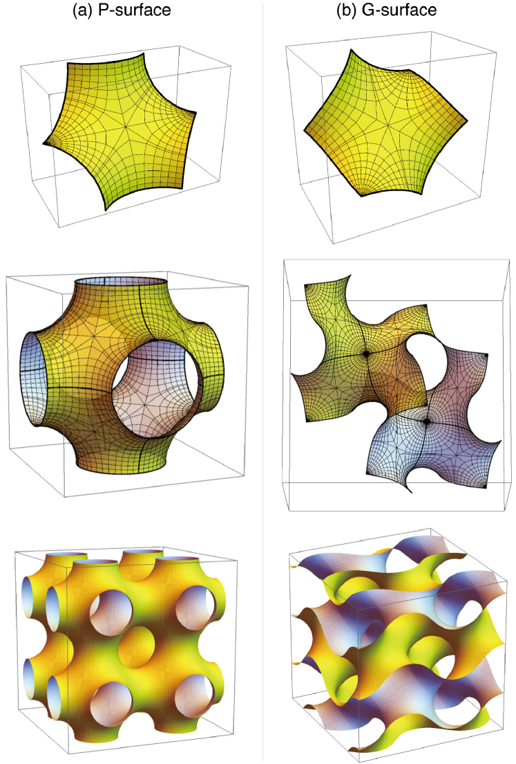
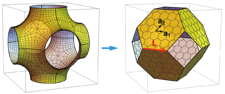
Formulation— P-surface (space group: Im3m) and G-surface (Iad) as networks of continuous membrane are depicted in Fig.1 (a) and (b), respectively. We can construct the 3D periodic structure from a primitive patch (top panel) to construct the 3D unit structure composed of eight primitive patches (middle panel), which are then periodically connected (bottom). Zeolitic graphites having the topologies of P or G-surfaces can then be constructed by taking a graphene fragment with a hexagonal shape as the primitive patch, as illustrated in Fig. 2 for P-surface. We can characterize the graphene fragment with indeces , which specify the lattice vector connecting the corners of the hexagon,
| (1) |
where and are primitive unit vectors of the original graphene honeycomb lattice. The resulting 3D structure has an eight-membered ring at each vertex where four patches meet, while it is composed of six-membered rings elsewhere. We can model the system with the simple tight-binding Hamiltonian for orbital of carbon, , where eV is the hopping integral, creates an electron on -th site, and are summed over nearest-neighbor sites. We neglect the curvature effect on the hopping parameter , and take it as a constant and the unit of energy ( eV). Effects of the curvature of the structure will be discussed below.
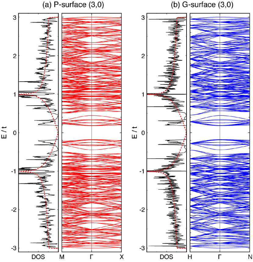
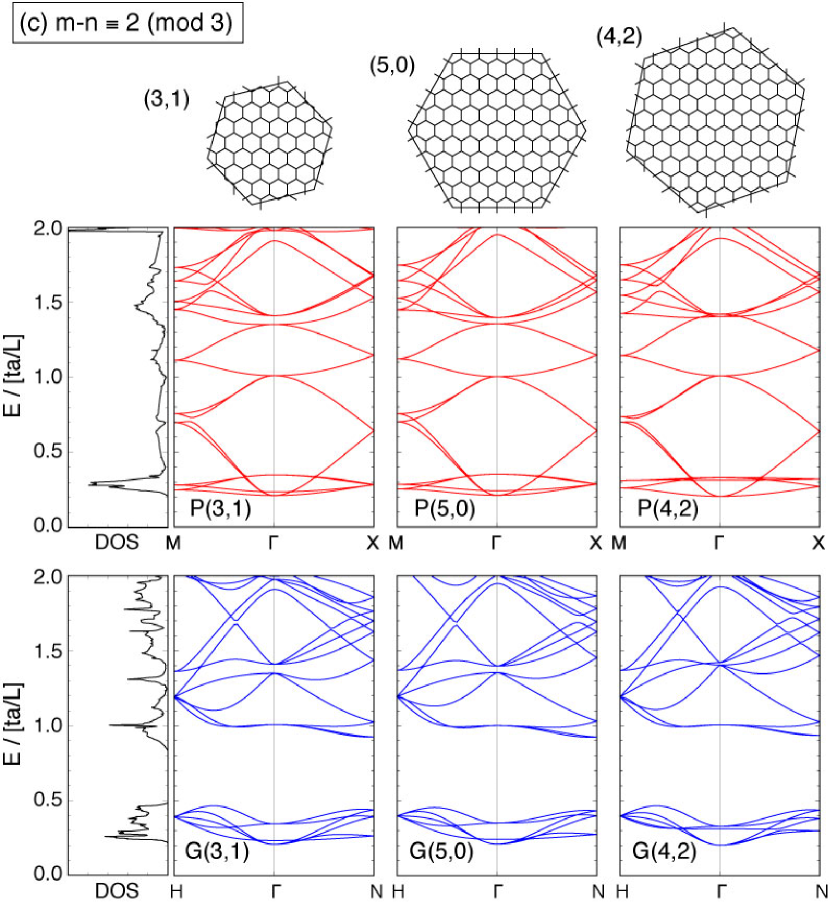
Results— Fig. 3 shows a typical band structure for (a) P-surface graphene and (b) G-surface graphene, here illustrated for . The spectrum is electron-hole symmetric with respect to (the charge neutrality point) in the present tight-binding model. Due to the band folding coming from the 3D periodicity, we have many bands, and if we look at the region around the charge neutrality point, the density of states (DOS) drastically deviates from graphene’s linear behavior (dashed curve). Specifically, the energy band is gapped around at , and some clustering is seen in the conduction (valence) bands just above (below) the gap.
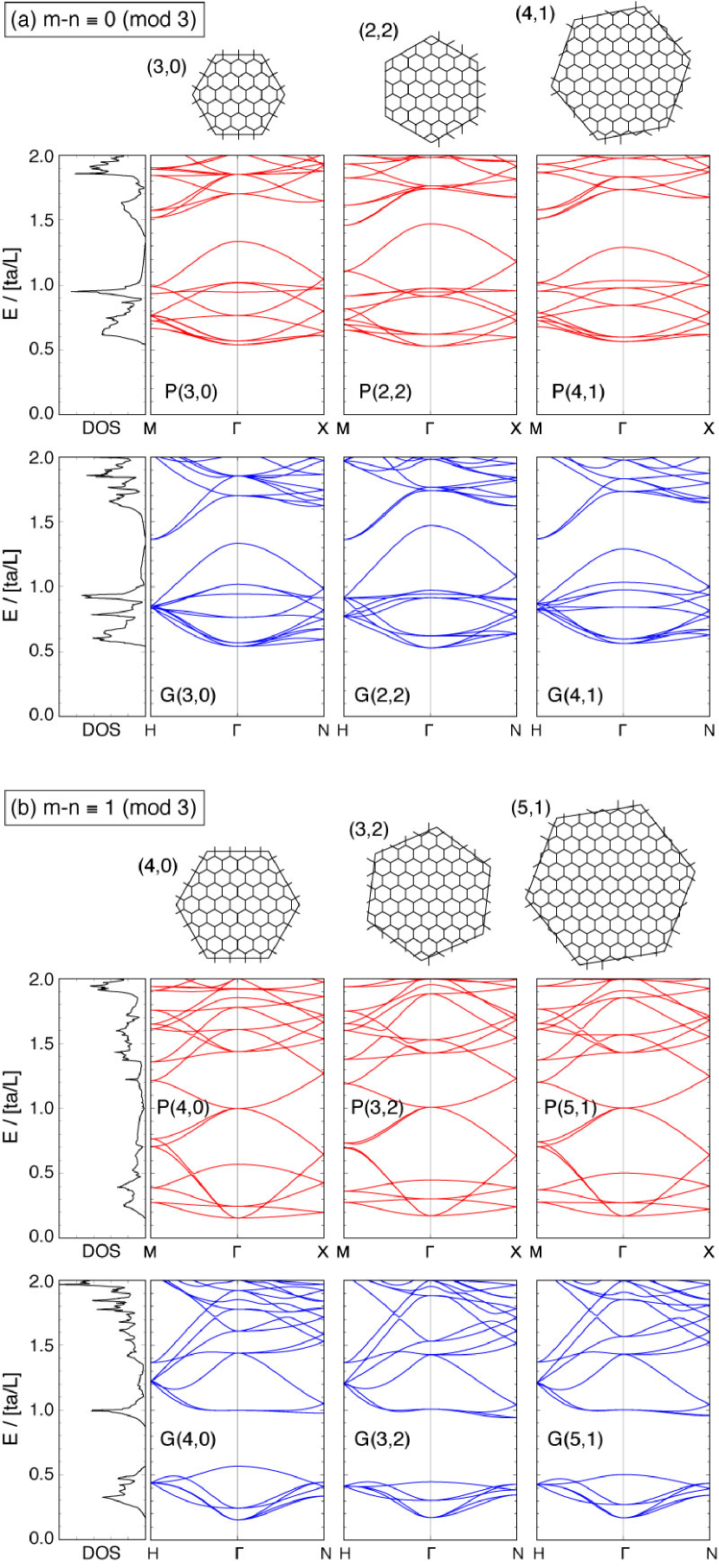
A fuller picture is shown for (mod 3) in Fig. 4(a), (Fig. 4(b)) and (Fig.5), for P-surface graphene (middle panels) and for G-surface graphene (bottom). For each case of (mod 3), we plot the results for three different choices of with the top inset showing the the primitive graphene fragment. Throughout, the energy is taken to be a dimensionless one, . This choice comes from our expectation that the low-energy spectrum around can be well described by the continuum massless Dirac field when the length scale of the 3D network is much longer than the atomic scale. Then the energy spectrum should be scaled as .
We clearly see that the rescaled band structures belonging to the same family [i.e., the same (mod 3) and the same surface topology (P or G)] are similar to each other, while distinct between different families. Specifically, the Dirac electron becomes massive, where the mass scales as . The modulo-3 rule is reminiscent of the situation in carbon nanotubesAndo2005 , and it is in fact an intrinsic property of graphitic systems having closed loop structures. In the flat graphene, the low-energy wave functions have a character of the states around the Brillouin zone corners , and when graphene is rolled into a carbon nanotube with circumference vector t, the wave function acquires a phase . Similarly, the 3D graphene network has a periodic array of close loops composed of hexagon’s sides, where similar phase factors emerge. The phase factor for a single side of hexagon [with the length L defined by Eq. (1)] amounts to , which is indeed determined solely by (mod 3), and explains the modulo-3 rule in the band structure. This situation around the Dirac point sharply contrasts with the those around the bottom (or top) of the whole energy spectrum (i.e. ), where we can show that the rescaled band structure only depends on the surface configuration (P or G), and does not depend on . This is because the bottom (or top) region corresponds to point of the original graphene,Aoki2002 where phase factors do not appear in the continuum model, and the characteristic energy scale is given by with being the -point effective mass.
If we now turn to the G-surface graphene, there is a specific interest as follows. In this “gyroid” structure, the surface has a screw axis along each of and directions. In fact the G-surface is the only triply-periodic surface having this property. The band structure of electrons has been analyzed by the present authors with Schrödinger equation KoshinoAoki2005 . There, we found that an effect of the helical structure appears as the multiple band sticking on the Brillouin zone boundaries. If we look at the present result for Dirac particles on G-surface, we immediately notice a salient feature that we have also multiple band sticking, which occurs for the Dirac particles at H point in the Brillouin zone and for the bunch of energy band just above the mass gap. In terms of the space group, this feature is expected to arise from a general property of non-symmorphic cases that promotes band touching Bradley1972 ; Parameswaran2013 .
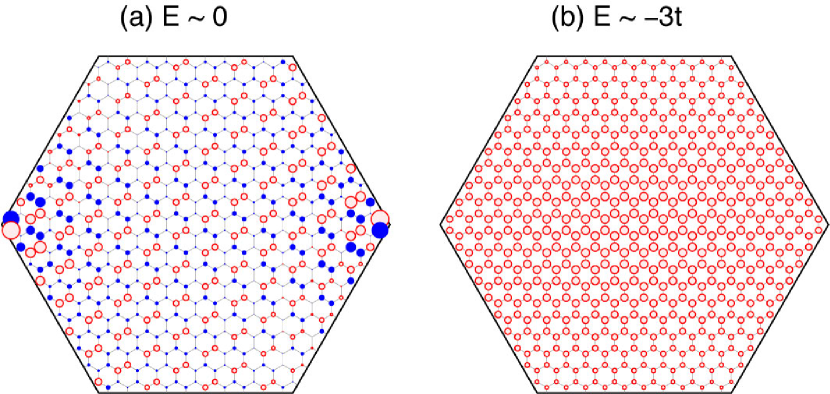
The wave functions also exhibit a notable feature. Figure 6 plots typical wave functions, here for , near (a) the charge neutrality point and near (b) the band bottom , both at -point in the 3D Brillouin zone. We can see that the wave function for has amplitudes sharply concentrated around the topological defects (which correspond to the corners of the patches), whereas that for is much more uniform. In the continuum Dirac field, the singular behavior around a more-than-six membered ring can be regarded as a consequence of the singular gauge fluxes, introduced in Ref. Gonzalez93, for 2D cases, that effectively thread topological defects in the honeycomb lattice. Thus the wave functions and band structures presented here should also be reproduced in a continuum Dirac model with these gauge fluxes included.
Finally, it should be mentioned that an electron confined to a curved graphene is generally affected by the local curvature neglected in the present model, where the hybridization between and occurs.Biase1994 In real 3D graphite sponges, the curvature is expected to be concentrated around the topological defects, and it would give additional resonant states as observed in the capped carbon nanotubes and the nanocones. Kim1999 ; Charlier2001
Conclusion— We have studied the electronic structure of 3D P- and G-surface graphene networks with various length scales. We find that the low-energy band structure is dominated by the topology of the structure, while within each topology the bands are basically determined by the periodicity in modulo 3. The 3D graphene hosts massive Dirac fermions, with the mass scaled as . In the present study, we considered the model which only includes eight-membered rings as topological defects. Very recent works studied various 3D carbon networks that include seven-membered rings, and found metallic band structure.Weng2014 ; Tagami2014 ; commentmetallic While their interest is focussed on smaller unit cell size atomic scale than in the present paper, it would be interesting to study the behavior of those classes of 3D graphites to examine how the metallic bands would scale with larger .
Let us make a few remarks on implications for experiments and future problems. Unlike the present theoretical model, the experimentally realized 3D graphene network is at present not periodic Ito2014 , but has a randomly connected structure. Still, we expect that singular wave amplitudes at the topological effects should be observed in the states around the charge neutrality point (i.e., when the system is not doped), as this is a topological property. The energy spectrum, on the other hand, should be different in the absence of periodicity, for which we would need some sort of the random network model combined with the Dirac equation, especially to analyze whether a (smeared) gap can appear at the Dirac point as in the periodic case.
The authors wish to thank Yoichi Tanabe, Yoshikazu Ito, and Mingwei Chen for helpful discussions and showing them some experimental results prior to publication. This work was supported by JSPS Grants-in-Aid for Scientific Research (Grants Nos. 25107005, 26247064).
References
- (1) For instance, helicoidal graphene [M. Watanabe, H. Komatsu, N. Tsuji and H. Aoki, to be published in Phys. Rev. B (arXiv:1505.05159)], and graphene ribbon with helicoidal geometries [V. Atanasov and A. Saxena, Phys. Rev. B 92, 035440 (2015)] have been considered.
- (2) H. W. Kroto, JR. Heath, S. C. O’Brien, R. F. Curl and R. E. Smalley, Nature 318 162, (1985).
- (3) S. Iijima, Nature, 354 56 (1991).
- (4) J. Gonzaléz, F. Guinea, and M.A.H. Vozmediano, Phys. Rev. Lett. 69, 172 (1992).
- (5) J. Gonzaléz, F. Guinea, and M.A.H. Vozmediano, Nucl. Phys. B 406, 771 (1993).
- (6) R. Tamura and M. Tsukada, Phys. Rev. B 49, 7697 (1994).
- (7) R. Tamura, K. Akagi, M. Tsukada, S. Itoh, and S. Ihara, Phys. Rev. B 56, 1404 (1997).
- (8) P. E. Lammert and V. H. Crespi, Phys. Rev. B 69, 035406 (2004).
- (9) H. Terrones and A. L. Mackay Nature, 352 762 (1991).
- (10) H. Terrones and A. L. Mackay Carbon, 30 1251 (1992).
- (11) D. Vanderbilt and J. Tersoff, Phys. Rev. Lett. 68, 511 (1992).
- (12) T. Lenosky, X. Gonze, M. Teter, and V. Elser, Nature 355, 333 (1992).
- (13) M. Fujita, T. Umeda, M. Yoshida, Phys. Rev. B 51, 13778 (1995).
- (14) H. Weng, Y. Liang, Q. Xu, R. Yu, Z. Fang, X. Dai, Y. Kawazoe, Phys. Rev. B 92, 045108 (2015).
- (15) M. Tagami, Y. Liang, H. Naito, Y. Kawazoe, M. Kotani, Carbon 76, 266 (2014).
- (16) H. Aoki, M. Koshino, D. Takeda, H. Morise and K. Kuroki, Phys. Rev. B 65, 035102 (2002).
- (17) H. Aoki, M. Koshino, D. Takeda, H. Morise, K. Kuroki, Physica E 22, 696 (2004).
- (18) M. Koshino and H. Aoki, Phys. Rev. B 71, 73405 (2005).
- (19) Z. Ma, T. Kyotani, Z. Liu, O. Terasaki and A. Tomita, Chem. Mater. 13, 4413 (2001).
- (20) Z. Ma, T. Kyotani and A. Tomita, Carbon 40, 2367 (2002).
- (21) H. Nishihara, Q.-H. Yang, P.-X. Hou, M. Unno, S. Yamauchi, R. Saito, J. I. Paredes, A. M. A. Nmnez-Alonso, J. M.D. Tasc Nsn, Y. Sato, M. Terauchi, T. Kyotani, Carbon 47, 1220 (2009).
- (22) W. Li, et al., Sci. Rep. 3, 2125 (2013).
- (23) Z-S. Wu et al., J. Am. Chem. Soc. 134, 19532 (2012).
- (24) Y. Xu et al., ACS Nano 7, 4042 (2013).
- (25) W. Chen, S. Li, C. Chen, L. Tan, Adv. Mater. 23, 5679 (2011).
- (26) X. Yang et al., Energy Storage, Science 341, 534 (2013).
- (27) Z. Chen et al., Nat. Mat. 10, 424 (2011).
- (28) X. Cao et al., Small 7, 3163, (2011).
- (29) Y. Ito et al., Angew. Chem. Int. Ed. 53, 4822 (2014).
- (30) T. Ando, J. Phys. Soc. Jpn. 74, 777 (2005).
- (31) C. J. Bradley and A. P. Cracknell, The Mathematical Theory of Symmetry in Solids (Clarendon Press, Oxford, 1972).
- (32) S. A. Parameswaran, A. M. Turner, D. P. Arovas, and A. Vishwanath, Nature Phys. 9, 299 (2013).
- (33) X. Blase, L. X. Benedict, E. L. Shirley, and S. G. Louie Phys. Rev. Lett. 72, 1878 (1994).
- (34) P. Kim, T. W. Odom, J.-L. Huang, and C. M. Lieber Phys. Rev. Lett. 82, 1225 (1999).
- (35) J.-C. Charlier and G.-M. Rignanese Phys. Rev. Lett. 86, 5970 (2001).
- (36) Two-dimensional, periodically perforated graphene can become metallic if odd-membered rings are present, as shown by N. Shima and H. Aoki, Phys. Rev. Lett. 71, 4389 (1993).