.
Probing quantum capacitance in a 3D topological insulator
Abstract
We measure the quantum capacitance and probe thus directly the electronic density of states of the high mobility, Dirac type of two-dimensional electron system, which forms on the surface of strained HgTe. Here we show that observed magneto-capacitance oscillations probe in contrast to magnetotransport - primarily the top surface. Capacitance measurements constitute thus a powerful tool to probe only one topological surface and to reconstruct its Landau level spectrum for different positions of the Fermi energy.
- PACS numbers
-
73.25.+i, 73.20.At, 73.43.-f
pacs:
1pacs:
2pacs:
3pacs:
1Three dimensional topological insulators (3D TI) represent a new class of materials with insulating bulk and conducting two-dimensional surface states Hasan and Kane (2010); Moore (2010); Qi and Zhang (2011); Ando (2013). The properties of these surface states are of particular interest as they have a spin degenerate, linear Dirac like dispersion with spins locked to their electron s -vector Ando (2013); Kane and Mele (2005). Strained epilayers of HgTe, examined here, constitute a 3D TI with high electron mobilities allowing the observation of Landau quantization and quantum Hall steps down to low magnetic fields Brune et al. (2011); Kozlov et al. (2014). While unstrained HgTe is a zero gap semiconductor with inverted band structure Groves et al. (1967); Seeger (1985), the degenerate states split and a gap opens at the Fermi energy if strained. This system is a strong topological insulator Fu and Kane (2007), explored so far by transport Brune et al. (2011); Kozlov et al. (2014); Brune et al. (2014), ARPES Crauste et al. (2013), photoconductivity and magneto-optical experiments Shuvaev et al. (2012, 2013a, 2013b); Dantscher et al. (2015); also the proximity effect at superconductor/HgTe has been investigated Sochnikov et al. (2015). Since these two-dimensional electron states (2DES) have high electron mobilities of several cm2/Vs, pronounced Shubnikov- de Haas (SdH) oscillations of the resistivity and quantized Hall plateaus commence in quantizing perpendicular magnetic fields Brune et al. (2011); Kozlov et al. (2014); Brune et al. (2014), stemming from both, top and bottom 2DES. The origin of the oscillatory resistivity is Landau quantization which strongly modifies the density of states (DoS). Capacitance spectroscopy allows to directly probe the thermodynamic DoS ( = carrier density, = electrochemical potential) denoted as , of a 3D TI. The total capacitance measured between a metallic top gate and a two-dimensional electron system (2DES) depends, besides the geometric capacitance, also on the quantum capacitance , connected in series and reflecting the finite density of states of the surface electrons Luryi (1988); Smith et al. (1986); Mosser et al. (1986); is the elementary charge. Below, the quantum capacitance of the top surface layer is denoted as , the one of the bottom layer by .
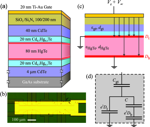
The experiments are carried out on strained 80 nm thick HgTe films, grown by molecular beam epitaxy on CdTe (013) Dantscher et al. (2015). The Dirac surface electrons have high electron mobilities of order cm2/Vs. The cross-section of the structure is sketched in Fig. 1a. For transport and capacitance measurements, carried out on one and the same device, the films were patterned into Hall bars with metallic top gates (Fig. 1b). For gating, two types of dielectric layers were used, giving similar results: 100 nm SiO2 and 200 nm of Si3N4 grown by chemical vapor deposition or 80 nm Al2O3 grown by atomic layer deposition. In both cases, TiAu was deposited as a metallic gate. The measurements were performed at temperature K and in magnetic fields up to 13 T. Several devices from the same wafer have been studied. For magnetotransport measurements standard lock-in technique has been applied with the excitation AC current of 10-100 nA and frequencies from 0.5 to 12 Hz. For the capacitance measurements we superimpose the dc bias voltage and a small ac bias voltage (see Fig. 1c) and measure the ac current flowing across our device phase sensitive using lock-in technique. The typical ac voltage was 50 mV at a frequency of 213 Hz. The absence of both leakage currents and resistive effects in the capacitance were controlled by the real part of the measured ac current. In order to avoid resistive effects in high magnetic fields additional measurements at lower frequencies (up to several Hz) were performed.
When the Fermi level (electrochemical potential) is located in the bulk gap the system can be viewed as a three-plate capacitor where the top and bottom surface electrons form the two lower plates (see Fig. 1c and the corresponding equivalent circuit in Fig. 1d). From this equivalent circuit follows that, as long as does not vanish, the measured total capacitance is more sensitive to changes of than of ; the explicit connection between , and the total capacitance is given in the Supplemental Material. The ratio of is significantly larger than unity since is (at ) at least a factor of two larger than . Here, is the geometric capacitance between top and bottom layer, with Baars and Sorger (1972), the dielectric constant of HgTe, is the thickness of the HgTe film, is the gated TI area and the dielectric constant of vacuum. Therefore, the measured capacitance reflects primarily the top surface s DoS, . In the limit (infinite distance to bottom surface) or () (no charge on bottom surface) the total capacitance is given by the expression usually used to extract the DoS of a two-dimensional electron system: with the geometric capacitance , where is the dielectric constant of the layers between gate and top 2DES, and , is the corresponding thickness Smith et al. (1986); Mosser et al. (1986). Note that therefore the variations of the DoS cause only small changes of the measured value of .
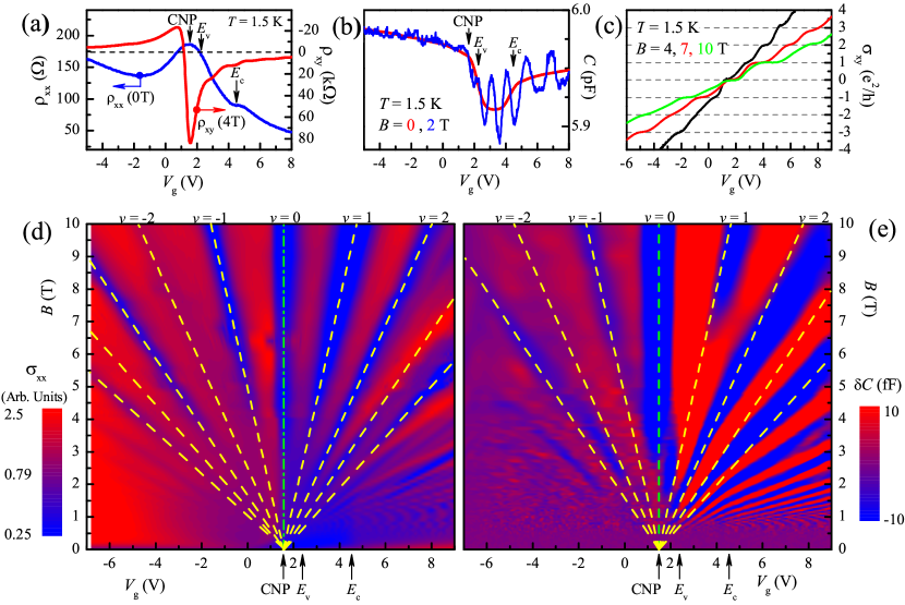
Typical and traces as function of the gate voltage are shown in Fig. 2a. displays a maximum near V, whereas changes sign; this occurs in the immediate vicinity of the charge neutrality point (CNP)Kozlov et al. (2014). The corresponding capacitance at in Fig. 2b exhibits a broad minimum between 2.2V̇ and 4.5 V and echoes the reduced density of states and of the Dirac 2DES when the Fermi energy is in the gap of HgTe. For V, moves into the conduction band where surface electrons coexist with the bulk ones. There, the capacitance (and thus the DoS) is increased and grows only weakly with increasing . Reducing below 2.2 V shifts below the valence band edge so that surface electrons and bulk holes coexist. A strong positive magnetoresistance, a non-linear Hall voltage and a strong temperature dependence of provide independent confirmation that is in the valence bandKozlov et al. (2014). Due to the valley degeneracy of holes in HgTe and the higher effective mass, the DoS, and therefore the measured capacitance is highest in the valence band.
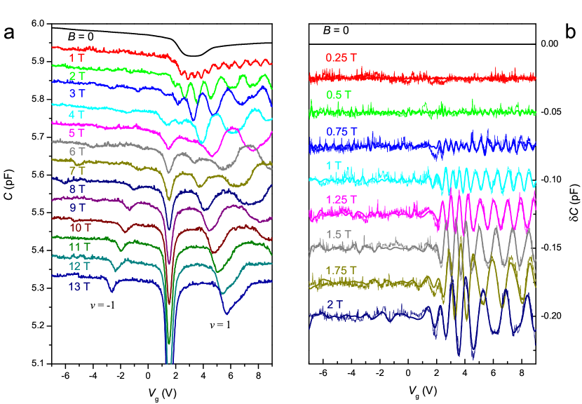
For well below 1 T both and start to oscillate and herald the formation of Landau levels (LLs). The trace oscillates around the zero field capacitance, shown for T in Fig. 2b. These oscillations, reflecting oscillations in the DoS, are more pronounced on the electron side (to the right of the CNP). This electron-hole asymmetry stems mainly from the larger hole mass, leading to reduced LL separation on the hole side. At higher fields Hall conductivity and resistivity (not shown) become fully quantized, for both electron and hole side. , shown for T, 7 T, and 10 T in Fig. 2c, shows quantized steps of height , ( = Planck s constant) as expected for spin-polarized 2DES.
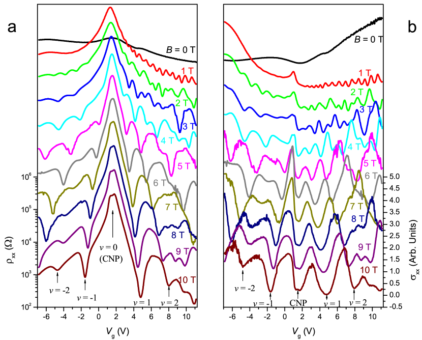
An overview of transport and capacitance data in the whole and space is presented in Figs. 3d and 3e as 2D color maps (see the Supplementary Material for additional data). We start with discussing the data, calculated from , in Fig. 2d first. The sequence of maxima and minima is almost symmetrical to the CNP where the electron and hole densities are equal. At fixed magnetic field the distance between neighboring minima corresponds to a change in a carrier density from which we can calculate, with the LL degeneracy , the filling rate cm-2/V at 10 T. Comparison of electron densities extracted in the classical Drude regime with densities taken from the periodicity of SdH oscillations have shown that oscillations at high reflect the total carrier density in the TI, i.e. charge carrier densities in the bulk plus in top and bottom surfaces Kozlov et al. (2014). We therefore conclude that the filling rate describes the change of the total carrier density with and is directly proportional to the capacitance per area . cm-2/V corresponds to a capacitance of F/m2, a value close to the calculated capacitance F/m2 using thickness and dielectric constant of the layers (see Figs. 1a and c and the Supplemental Material). Using this extracted at 10 T, the Landau level fan chart, i.e. the calculated positions of the minima as function of and , fits the data for low filling factors quite well. For filling factors larger than on the electron side the fan chart significantly deviates from experiment and is discussed using higher resolution data below. On the hole side where the SdH oscillations stem from bulk holes, fan chart and experimental data match almost over the whole range. Remarkably, minima corresponding to odd filling factors are more pronounced than even ones, reflecting the large hole -factor. We now turn to the magneto-capacitance data shown in Fig. 2e. The data are compared with the same fan chart derived from transport. On the electron side, the experimental minima display a reduced slope compared to the calculated fan chart, pointing to a reduced filling rate. This is a first indication that the capacitance does not reflect the total carrier density in the system but predominantly the fraction of the top 2DES only. On the hole side the LL fan chart fits the data quite well but in contrast to transport, LL features are less well resolved there. This asymmetry is connected to the different effective masses; the enhanced visibility in transport is due to that fact that SdH oscillations depend on while the capacitance depends on only.
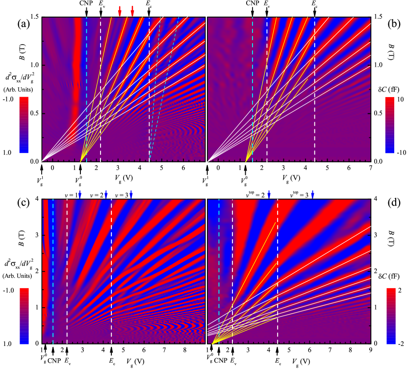
Previous transport experiments have shown that the periodicity of the SdH oscillations is changed at low magnetic fields, reflecting a reduced carrier density. Tentatively, this was ascribed to SdH oscillations stemming from the top surface only Kozlov et al. (2014). When top and bottom surface electrons have different electron densities and mobilities it is expected that Landau level splitting - in sufficiently low - is in transport first resolved for the layer with the higher density and mobility, i.e. higher partial conductivity and lower LL level broadening. This expectation is consistent with previous experimental observation Kozlov et al. (2014). If, indeed, the low field SdH oscillations resemble the carrier density of a single Dirac surface, capacitance oscillations which probe preferentially the top surface and SdH oscillations should have the same period. Thus we compare and capacitance in Fig. 3a and 3b at low up to 1.5 T. In this low field region the capacitance (Fig. 3b) shows overall uniform oscillations of . The position of the maxima, corresponding to different LLs, is perfectly fitted by two fan charts featuring a distinct crossover at about V. The crossover is due to entering the conduction band which causes a reduced filling rate of the electrons responsible for the quantum oscillations at V. Apparently, the quantum oscillations are caused by the top surface electrons only while the bulk electrons and electrons on the bottom surface merely act as a reservoir. Note, that the filling rate into the top surface state, probed in experiment, gets reduced when the filling rate into bulk states , since the total filling rate must be constant Kozlov et al. (2014). From the distance of maxima at constant we can extract the filling rate in the gap (2.2 V 4.4 V) and when is in the conduction band, . From Fig. 3b we obtain cm-2/V and cm-2/V. This means that in the gap % of the total filling rate apply to the top surface while the remaining 30 % can be ascribed to the bottom surface. The reduced filling rate for in the conduction band is and hence the remaining filling rate of 56 % is shared between bulk and back surface filling. We note that we obtain reasonable values for the filling rates only when we assume spin-resolved LL degeneracy. Since there is no signature of spin splitting down to 0.6 T, where the oscillations get no longer resolved one can conclude that the quantum oscillations always stem from non-degenerate LLs, proving the topological nature of the charge carriers. The extrapolation of the two fan charts towards defines two specific points on the -axis, denoted as V and V. These points correspond to vanishing electron density on the top surface in case the respective filling rates and would stay constant over the entire range. This is not the case as only applies for in the conduction band and for in the gap. Moving into the valence band greatly reduces this filling rate. Therefore and correspond only to virtual zeroes of the electron density while the real one is much deeper in the valence band.
To get a better resolution of the low field SdH oscillation we plot in Fig. 3a; as before red regions indicate maxima. The same LL fan chart in Figs. 3b and 3a, fits both, transport and capacitance, quite well. Hence, at sufficiently low , both and oscillations resemble the carrier density of the top surface only. However, even at low striking deviations in pop up which get more pronounced at higher (see below). Two faint lines at T and V which appear between the LLs of the top surface and are marked by red arrows in Fig. 3a, are ascribed to SdH oscillations stemming from the bottom surface. More differences occur once enters the conduction band ( V). New maxima appear in the fan chart and form rhomb like structures. These anomalous structures, completely absent in capacitance, get even more intriguing at higher , displayed in Fig. 3c. Data taken at up to 4 T, displayed in Figs. 3c and 3d, show marked differences between transport and capacitance. maxima, given by the red regions in Fig. 3d are, as before, well described by the same two LL fan chart with the same filling rates as in Figs. 3a and b. The filling factors given on top of Fig. 3d are the ones of the electrons in the top surface only, while the filling factors given in Fig. 3c are the ones of the total carrier density, determined by the total filling rate and the position of the plateaus in Fig. 2c. The transport data for in the gap show splitting of the Landau levels and for V, i.e. for in the conduction band, a very complex structure with crossing LLs evolves, which is strikingly different from the one observed in the capacitance data. We thus conclude that in transport experiments the three available transport channels (top, bottom surface electrons, bulk electrons) contribute to the signal and lead to a complicated pattern of the quantum oscillations as a function of and . The oscillations of the quantum capacitance, in contrast, stem preferentially from the top surface and allow probing the LL spectrum of a single Dirac surface in a wide range of and . Corrections to that likely occur at high and : a level splitting at ( V, T) in Fig. 3d suggest that signals from bulk or back surface can affect also at higher , although to a far lesser degree when compared to transport.
In summary, we present first measurements of the quantum capacitance of a TI which directly reflect the DoS of Dirac surface states. The oscillations of the quantum capacitance in quantizing magnetic fields allow tracing the LL structure of a single Dirac surface. The complimentary information provided by transport and capacitance experiments is promising in getting a better understanding of the electronic structure of TIs, the latter being particularly important for potential applications of this new class of materials.
Acknowledgements.
We acknowledge funding by the Elite Network of Bavaria and by the German Science Foundation via SPP 1666. This work was partially supported by RFBR grants No 14-02-31631, 15-32-20828 and 15-52-16008. Supplementary Information: “Probing quantum capacitance in a 3D topological insulator” D. A. Kozlov, D. Bauer, J. Ziegler, R. Fischer, M. L. Savchenko, Z. D. Kvon, N. N. Mikhailov, S. A. Dvoretsky and D. WeissI Samples details
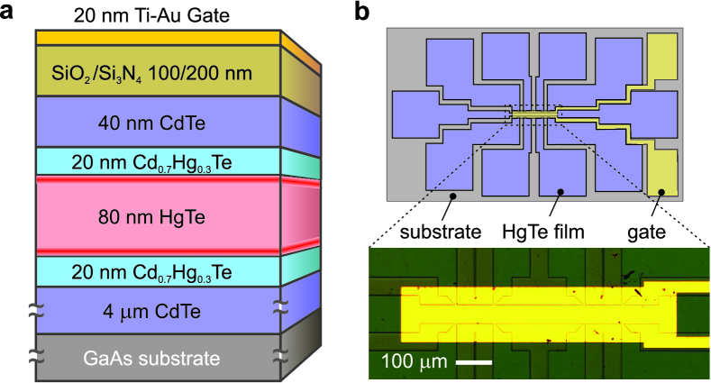
The experiments were carried out on strained 80 nm thick HgTe films, grown by molecular beam epitaxy (MBE) on CdTe (013) Dantscher et al. (2015). The Dirac surface electrons have high electron mobilities of order m2/Vs Kozlov et al. (2014). The cross section of a structure is sketched in Fig. S4a. For transport and capacitance measurements, carried out on one and the same device, the films were patterned into Hall bars with metallic top gates (Fig. S4b).
For gating, two types of dielectric layers were used, giving similar results: 100 nm SiO2 and 200 nm of Si3N4 grown by chemical vapor deposition or 80 nm Al2O3 grown by atomic layer deposition (not shown in Fig. S4a). In both cases, TiAu was deposited as a metallic gate. The measurements of the total capacitance between the gate and the HgTe layer were performed at temperature K and in magnetic fields up to 13 T. Several devices from the same wafer have been studied. For magnetotransport measurements standard lock-in technique has been applied with excitation AC currents of 10-100 nA at frequencies ranging from 0.5 to 12 Hz. For the capacitance measurements we superimpose the DC bias voltage with a small AC bias voltage (see Fig. 2c) and measure with lock-in technique the AC current flowing across our device phase sensitively. The typical AC voltage was 50 mV at a frequency of 213 Hz. The absence of both leakage currents and resistive effects in the capacitance were controlled by the real part of the measured AC current. These resistive effects occur when the condition becomes invalid, for example when the series resistance , i.e. the resistance of the two-dimensional electron gas increases at integer filling factors and high magnetic fields. In order to suppress resistive effects in high magnetic fields additional measurements at lower frequencies (down to several Hz) were performed (see below).
II Samples band diagram and equivalent circuit
II.1 Electrostatic and band diagram
Following the papers of Stern Stern (1983), Smith Smith et al. (1985) and Luryi Luryi (1988) we introduce an equivalent circuit for the sample’s capacitance based on simple one-dimensional electrostatics. The discussion is limited to the case where the Fermi level is located in the gap, so that contributions of bulk holes and electrons are absent. The top and bottom surface layers are treated as infinitely thin, negatively charged surfaces with finite density of states (DoS), i.e. we ignored the spatial distribution of the surface electrons. Finally, we treated the insulating layer as uniform with an average dielectric constant and with the total thickness of the layers given in Fig. S4.
A cartoon of the resulting simplified band diagram is presented for zero gate voltage in Fig. S5a. Without applied the Fermi level is constant across the structure. The density of electrons and on top and bottom surface, respectively, depends on the position of the Fermi level with respect to the Dirac point (which is, other than sketched in Fig. S5a below the valence band edge). For the sake of simplicity we assume that the densities are the same at . This simplification is justified since we are only interested in changes of the carrier density with gate voltage and not in absolute values of the carrier density.
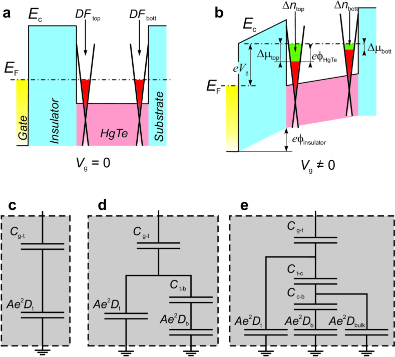
For an applied gate voltage we assume that the voltage drop occurs exclusively across the SiO2/Si3N4 insulator leading to an energy difference between the Fermi level in the gate metal and the HgTe layer. Here, is the elementary charge. Applying a positive gate voltage increases the carrier density in top and bottom layer by and , respectively. Due to screening of the electric field by the top surface layer the induced electron density is higher in the top layer than in the bottom one; while the Fermi level throughout the HgTe layer is constant the different electron density in top and bottom surface layer causes an electrical potential drop between bottom and top surfaces of . The change of carrier density in top and bottom layer can be written as , where is the density of states (DoS) of the electrons on the top (bottom) surface. Thus the following relation holds:
| (1) |
Using charge neutrality and Gauss’s law of electrostatics the potential drop in the HgTe layer can be calculated from the electric field , induced by the additional electron density on the bottom layer:
| (2) |
is the dielectric constant of HgTe and is the distance between the electron wave functions of top and bottom surfaces layers, approximated by the thickness of the HgTe layer, . Combining formulas 1 and 2 gives a relation between and :
| (3) |
This is the expression given by Luryi Luryi (1988) generalized for non-parabolic dispersion of the surface electrons.
II.2 The equivalent circuit
In the main text we discuss the equivalent circuit of a three plate capacitor as a model for the capacitance measured in a topological insulator with metallic gate and top and bottom surface layers. The equivalent circuit is applicable when the Fermi level is in the bulk gap of HgTe and is shown in Fig. 1d and the Supplementary Figure S5d. A similar equivalent circuit has been recently suggested for the same system but a slightly different configuration Baum et al. (2014). The four capacitors drawn in Supplementary Figure S5d represent either geometrical ( and ) or quantum ( and ) capacitances. Here, is the geometrical capacitance associated with the insulating layer between the gate and the top surface of the HgTe layer; is responsible for the potential drop across the HgTe layer between electrons on the top and bottom surface; and are the corresponding quantum capacitances representing the finite DoS of the corresponding HgTe surface states; in all cases is the gate area. The equivalent circuit in Fig. S5d describes the electrostatics of the system: Indeed, the charge on the quantum capacitors is the one induced by the gate voltage, and and the voltage across the geometrical ones is, as it should be, proportional to the corresponding induced charge and the thickness of the respective dielectric layer.
The circuit becomes simpler if one removes the influence of the bottom surface: this can be done by increasing the distance between top and bottom layer () or by removing the charge carriers (). Then only two capacitors are present in the reduced circuit (Fig. S5c); this is the situation relevant for a gated two-dimensional electron system. In contrast, if the Fermi level is lying in the bulk electron or hole band (see Fig. S5e) the situation becomes more complex. In this case bulk carriers are characterized by a particular wave function across the HgTe layer. A simple approach to model this is to replace the capacitor by two capacitors and representing the potential drop between the maximum of the bulk carriers’ wave function (denoted by subscript ”c” at a point around the center of the HgTe layer) and the top and bottom of the HgTe layer, respectively. For this the relation holds.
The total sample’s capacitance for the circuit shown in Fig. S5c can be easily derived using Ohm’s law and is given by:
| (4) |
In the actual device the relation holds, therefore and any variation of the DoS, e.g. in a magnetic field, leads only to a small change of the total capacitance . An important result which can be derived from Eq. 4 is the sensitivity of the total capacitance to a change of the DoS of top and bottom layer, and , respectively:
| (5) |
| (6) |
The ratio of both quantities
| (7) |
is always larger than 1 as long as which means that the total capacitance is more sensitive to oscillations of the top layer, e.g., the same oscillation amplitude of and will lead to significantly different oscillation amplitudes in the measured total capacitance .
II.3 Numeric evaluations
Here, we provide the values of the capacitances of our devices. The insulating layer underneath the metallic gate consists of Si3N4 (200 nm layer with ), SiO2 (100 nm with ), CdTe (40 nm with ), CdHgTe (20 nm with ) and HgTe (5-7 nm with ) and F/mm2. The calculated value of the specific geometrical capacitance is very close to the experimental one, F/mm2 obtained from the filling rate cm-2/Vs (see main text).
Using the gate area mm2 (see Fig. S4b) the sample’s geometric capacitance is expected to be pF which is in line with the measured value ( pF) if one subtracts the parasitic capacitance of our set up, being around 17 pF.
With the known values of the surface electrons’ effective mass Dantscher et al. (2015) one can estimate the specific quantum capacitances: F/mm2 which is almost two orders of magnitude higher than the specific geometrical capacitance .
Finally, the evaluated specific capacitance of the nm thick HgTe layer with is F/mm2. From this value and with Eq. 3 one can derive the relation between filling rates of electrons on top and bottom surfaces: . However, in our experiment, described in the main text, we obtain , and . This discrepancy suggests that the equivalent circuit in Fig. S5d does not fully describe the experimental situation. Most likely this deviation stems from the fact that we neglected the dependence of the surface states’ dispersion on the transversal electric field described in Brune et al. (2014). Phenomenologically, this shortcoming can be corrected by introducing a larger effective capacitance of F/mm2, indicating an enhanced screening in HgTe. This can be achieved by a higher value of the dielectric constant of HgTe or a reduced effective layer thickness.
We note that for both values of given above, the ratio is larger than 5.5, meaning that the sample capacitance is predominantly sensitive to changes of the DoS of the top surface.
III Densities and partial filling rates
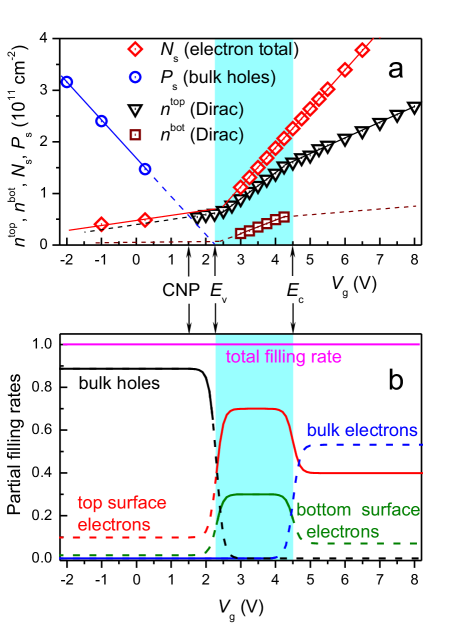
The gate voltage dependence of the different carrier species is shown in Fig. S6a. The total electron density and the bulk hole density were obtained from the low field transport data using the classical (two-carrier) Drude model as described in Kozlov et al. (2014). The top surface electron density was obtained from the periodicity of the capacitance oscillations, , with the period on the scale and Planck’s constant . For this technique is not applicable since the oscillations are dominated by bulk holes. The density of the bottom surface electrons was obtained from which holds as long as is located in the bulk gap, i.e. V. In our experiment it is impossible to directly measure the density of electrons on the bottom surface since their response is masked by electrons on the top surface. Consequently the value of can not be derived when the Fermi level is in the valence (because of unknown value of ) or the conductance band (because of the unknown value of ). However, based on the equivalent circuit shown in Fig. S5d and e one can make an educated guess on the partial filing rates. The result of such analysis is shown in Fig. S6b.
IV Resistive effects in the capacitance
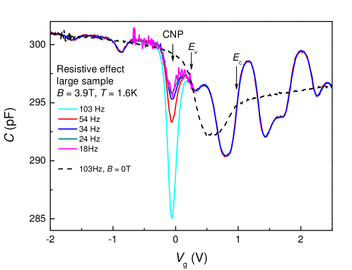
As mentioned in the main text, resistive effects occur when the condition becomes invalid, for example when the resistance of a two-dimensional electron gas connected in series to the capacitance increases at integer filling factors and high magnetic fields. The absence of both leakage currents and resistive effects in the capacitance were controlled by the real part of the measured AC current. A direct manifestation of resistive effects is the frequency-dependence of the measured traces. A corresponding example, taken from a sample with larger gate area and therefore larger capacitance is shown in Fig. S7. The capacitance minimum appearing at the charge neutrality point (CNP) and connected to a gap opening at higher magnetic fields shows a pronounced frequency dependence. The resistive effects are weak up to 34 Hz. With increasing frequency, however, the minimum becomes deeper and the capacitance signal no longer reflects the density of states. Remarkably, in all our samples the resistive effects first appear close the CNP and are much less pronounced at integer filling factors at the same values of magnetic field. Thus the remaining capacitance oscillations reflect the density of states.
V Experimental Data
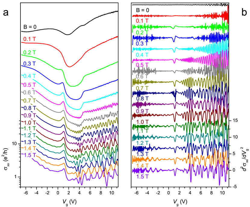
In this section we show some of the raw data and outline how they were prepared for the color maps in the main article. Fig. S8a displays the capacitance as a function of gate voltage and for magnetic fields between 0 and 13 T. In the color maps we plot the differential magnetocapacitance , shown for magnetic fields up to 2 T in Fig. S8b. In order to suppress the noise we used standard band-pass Fourier filtering with the cutoff frequencies T-1 and T-1 depending on the magnetic field range.
The corresponding transport data measured on the same device are plotted in Fig. S9a. Together with the corresponding traces (not shown) the resistivity data were converted into traces shown in Fig. S9b. Since the value of varies over several orders of magnitude and in order to improve the clarity of the color maps (Fig. 3d) each trace was normalized with respect to its average value using , where means averaging over the whole range. After the normalization procedure the average value of each trace is equal to 1.
The data taken at lower magnetic fields are shown in the Fig. S10a. To work out the oscillations more clearly we plot the second derivative of the traces, shown in panel a of Fig. S10b. In order to visualize the low-field oscillations clearly on the color maps each trace was normalized by its root mean square (RMS) value taken over the whole scale. Finally we applied standard low-pass Fourier filtering to remove random noise which is quite pronounced for the lowest field ( T) traces.
References
- Hasan and Kane (2010) M. Z. Hasan and C. L. Kane, Rev. Mod. Phys. 82, 3045 (2010).
- Moore (2010) J. E. Moore, Nature 464, 194 (2010).
- Qi and Zhang (2011) X.-L. Qi and S.-C. Zhang, Rev. Mod. Phys. 83, 1057 (2011).
- Ando (2013) Y. Ando, J. Phys. Soc. Jpn. 82, 102001 (2013).
- Kane and Mele (2005) C. L. Kane and E. J. Mele, Phys. Rev. Lett. 95, 226801 (2005).
- Brune et al. (2011) C. Brune, C. X. Liu, E. G. Novik, E. M. Hankiewicz, H. Buhmann, Y. L. Chen, X. L. Qi, Z. X. Shen, S. C. Zhang, and L. W. Molenkamp, Phys. Rev. Lett. 106, 126803 (2011).
- Kozlov et al. (2014) D. A. Kozlov, Z. D. Kvon, E. B. Olshanetsky, N. N. Mikhailov, S. A. Dvoretsky, and D. Weiss, Phys. Rev. Lett. 112, 196801 (2014).
- Groves et al. (1967) S. H. Groves, R. N. Brown, and C. R. Pidgeon, Phys. Rev. 161, 779 (1967).
- Seeger (1985) K. Seeger, Semiconductor Physics (Springer Series in Solid State Sciences 40, 1985).
- Fu and Kane (2007) L. Fu and C. L. Kane, Phys. Rev. B 76, 045302 (2007).
- Brune et al. (2014) C. Brune, C. Thienel, M. Stuiber, J. Bottcher, H. Buhmann, E. G. Novik, C.-X. Liu, E. M. Hankiewicz, and L. W. Molenkamp, Phys. Rev. X 4, 041045 (2014).
- Crauste et al. (2013) O. Crauste, Y. Ohtsubo, P. Ballet, P. A. L. Delplace, D. Carpentier, C. Bouvier, T. Meunier, A. Taleb-Ibrahimi, and L. Levy, arXiv:1307.2008 (2013).
- Shuvaev et al. (2012) A. M. Shuvaev, G. V. Astakhov, C. Brune, H. Buhmann, L. W. Molenkamp, and A. Pimenov, Semicond. Sci. Technol. 27, 124004 (2012).
- Shuvaev et al. (2013a) A. M. Shuvaev, G. V. Astakhov, M. Muhlbauer, C. Brune, H. Buhmann, and L. W. Molenkamp, Appl. Phys. Lett. 102, 241902 (2013a).
- Shuvaev et al. (2013b) A. M. Shuvaev, G. V. Astakhov, G. Tkachov, C. Brune, H. Buhmann, L. W. Molenkamp, and A. Pimenov, Phys. Rev. B 87, 121104(R) (2013b).
- Dantscher et al. (2015) K.-M. Dantscher, D. A. Kozlov, P. Olbrich, C. Zoth, P. Faltermeier, M. Lindner, G. V. Budkin, S. A. Tarasenko, V. V. Belkov, Z. D. Kvon, N. N. Mikhailov, S. A. Dvoretsky, D. Weiss, B. Jenichen, and S. D. Ganichev, Phys. Rev. B / arXiv:1503.06951 accepted, accepted (2015).
- Sochnikov et al. (2015) I. Sochnikov, L. Maier, C. A. Watson, J. R. Kirtley, C. Gould, G. Tkachov, E. M. Hankiewicz, C. Brune, H. Buhmann, L. W. Molenkamp, and K. A. Moler, Phys. Rev. Lett. 114, 066801 (2015).
- Luryi (1988) S. Luryi, Appl. Phys. Lett. 52, 501 (1988).
- Smith et al. (1986) T. P. Smith, W. I. Wang, and P. J. Stiles, Phys. Rev. B 34, 2995 (1986).
- Mosser et al. (1986) V. Mosser, D. Weiss, K. v Klitzing, K. Ploog, and G. Weimann, Solid State Commun. 58, 5 (1986).
- Baum et al. (2014) Y. Baum, J. Bottcher, C. Brune, C. Thienel, L. W. Molenkamp, A. Stern, and E. M. Hankiewicz, Phys. Rev. B 89, 245136 (2014).
- Baars and Sorger (1972) J. Baars and F. Sorger, Solid State Commun. 10, 875 (1972).
- Stern (1983) F. Stern, Appl. Phys. Lett. 43 (10), 974 (1983).
- Smith et al. (1985) T. P. Smith, B. B. Goldberg, P. J. Stiles, and M. Heiblum, Phys. Rev. B 32 (4), 2696 (1985).