Magnetotransport in Double Quantum Well with Inverted Energy Spectrum: HgTe/CdHgTe
Abstract
We present the first experimental study of the double-quantum-well (DQW) system made of 2D layers with inverted energy band spectrum: HgTe. The magnetotransport reveals a considerably larger overlap of the conduction and valence subbands than in known HgTe single quantum wells (QW), which may be regulated in some extent by an applied gate voltage . This large overlap manifests itself in a much higher critical field separating the range above it where the quantum peculiarities shift linearly with and the range below with a complicated behavior. In the latter case the -shaped and double--shaped structures in the Hall magnetoresistance are observed with their scale in field pronouncedly enlarged as compared to the pictures observed in an analogous single QW. The coexisting electrons and holes were found in the whole investigated range of positive and negative as revealed (i) from fits to the low-field -shaped , (ii) from the Fourier analysis of oscillations in and (iii) from a specific behavior of the quantum Hall effect. A peculiar feature here is that the found electron density remains almost constant in the whole range of investigated while the hole density drops down from the value a factor of 6 larger than at extreme negative to almost zero at extreme positive passing through the charge neutrality point. We show that this difference between and stems from an order of magnitude larger density of states for holes in the lateral valence band maxima than for electrons in the conduction band minimum. We interpret the observed reentrant sign-alternating between electronic and hole conductivities and its zero resistivity state in the quantum Hall range of fields on the basis of a calculated picture of magnetic levels in a DQW. This behavior is due to (i) an oscillating of the valence subband top versus field in the overall picture of its magnetic levels, (ii) a reduced gap between the lowest electron and the highest hole magnetic levels where the electron- and hole-type localized states are superposed, and (iii) a possible formation of the interlayer electron-hole excitons.
pacs:
73.21.Fg, 73.43.-f, 73.43.Qt, 73.43.NqI Introduction
Spatially quantized energy spectrum of the HgTe layer wider than nm is markedly specific due to its inversion character.Konig In this case the conduction and valence subbands are close in energy due to their quasidegeneracy and for nm both are built of the -symmetry wave functions contrary to the traditional semiconductor structures with their finite intrinsic gap and a conduction subband of the character. Moreover, the conduction subband may overlap here with the lateral maxima of the valence subbandKvon JETPLett2008 leading to formation of a semimetal with coexisting electrons and holes. The overlap occurs in a relatively wide HgTe quantum well (QW) depending on the heterostructure characteristics, of which probably the main is the built-in deformation.Kvon PRB2011 ; Olshanetsky SSC2012 Diverse new physics arises in such a semimetal. For example, correlations between the electron and hole subsystems may cause a transition into a state of exciton insulatorOlshanetskyJETPL2013 while the enhanced electron-hole friction in this situation results in modified temperature dependencies of transport coefficients.EntinJETP2013 The picture of magnetic levels in this semimetal is very intricate as it consists of two overlapped fan-charts oppositely directed in energy. Additional complications appear here due to existence of specific zero-mode levels of a strongly mixed electron-hole nature in each subband and due to a nonmonotonous behavior of the valence subband levels around the energy of lateral maxima. A gap is opened between the lowest electron magnetic level and the highest hole levels at some critical magnetic field thus creating a possibility to realize a unique zero filling factor state when the Fermi level gets into this gap.Gusev-2010 ; Raichev-2012 This state has also been revealed in graphene and has been actively debated.Zhang2006 The specific shape of the valence subband with a central minimum and lateral maxima causes an oscillating-like behavior of the subband top profile vs. quantizing magnetic field. These oscillations may be felt in the quantum magnetotransport once their scale is comparable with the typical distances between the valence subband levels when the quantum features connected with these levels are resolved experimentally. Physics get especially unusual here because of a possible competition between the states of a heavy electron character in the central valence subband minimum and the hole states around its lateral maxima and at larger wave vector values.
We present our investigations of a technique to change and regulate in situ the subband overlap using a system of two relatively wide HgTe quasi-2D layers separated by a thin CdHgTe barrier, i.e., a HgTe double quantum well (DQW) with inverted energy spectrum. Application of a gate voltage causes a shift of the whole energy spectrum picture in the upper HgTe layer (which is closer to the gate) with respect to a similar energy spectrum of the lower HgTe layer, since the free charges in the upper layer screen the lower layer so that its energy is almost insensitive to .DQWlayershifts It results in a change of the overlap between the conduction () subband in one layer and the valence () subband in the other. The HgTe/CdHgTe system is specific in this sense differing from a traditional DQW, e.g., the GaAs/AlGaAs system, since for normal gaped semiconductors the interlayer overlap occurs only for the same kind of bands: or . In a DQW of traditional semiconductors the exhaustion of the upper layer may be achieved, after what the charge density in the lower layer starts to vary with .DQWlayershifts In contrast, the exhaustion of the upper layer would never come in a HgTe layer, only the kind of free charges will be changed here when the Fermi level moves between the touched or overlapped - and -bands.
An exclusion is the InAs/GaSb system where two normal spectra are intrinsically so much shifted in energy that the InAs -band falls below the GaSb -band top.Nicholas-2000 ; Suzuki-2003 However, a substantial interlayer hybridization gap appears in this system, which considerably modifies the collective energy spectrum. Also, a balanced state with equal electron and hole densities (a charge neutrality point, CNP), which is one of the most remarkable moments in a system with overlapped - and -bands, has not been reached in InAs/GaSb system so far.Suzuki-2004
Although the overlap of and bands occurs in our case between the layers, it affects interlayer electron–hole () interactions in the DQW with a thin enough barrier thus predetermining magnetotransport in the whole system. Variation of in a DQW provides some new opportunities to scan the complicated structure of the valence subband top by the Fermi level. Information about the valence subband top in the case of overlapped bands is especially actual since some controversy about its structure has been revealed recently.Minkov-2013
Other important aspects of the HgTe DQW are caused by the fact that the magnetic levels of different momentum projections in the conduction subband, which are analogs of the spin sublevels in a band, are easily resolvable here indicating a large effective -factorYaPE2010 and leading to well pronounced effects of spin polarization,YaPRB2012 i.e., to a good realization of the spin degree of freedom. It invokes a question: how would manifest itself such an unusual combination of the HgTe layer characteristics in the collective electronic properties of DQW? Existence of an additional pseudospin degree of freedom connected with the possibility for an electron to reside in one of the two interconnected layers is known to result in a formation of new correlated states of the electronic systemGirvin or in a improved stabilization of the correlated states known in a single QW as a quantum Wigner solid.Manoharan-96 Also shown wasGiudici-2008 that a well pronounced spin degree of freedom plays a positive role in formation of correlated phases. Would the -orbitals of the HgTe conduction and valence subbands introduce some novel features in the possible correlation effects? Would the addition of one more degree of freedom – a well pronounced effective spin degree – manifest itself here? The interest to these subjects is still enhanced by the predictionMichetti-Novik2012-2014 that a special kind of topological insulator may be created in the HgTe DQW with a perspective of its utilization in spintronics devices. We are doing the experimental attempts to answer some of these questions as presented in this work.
II Experimental details
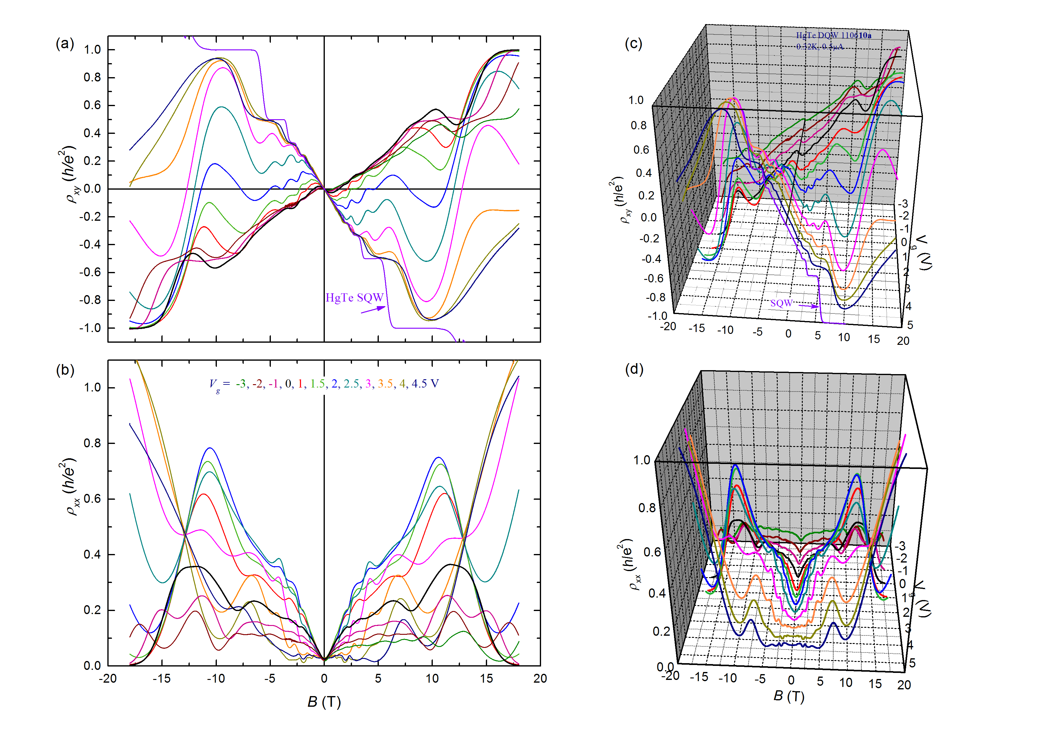
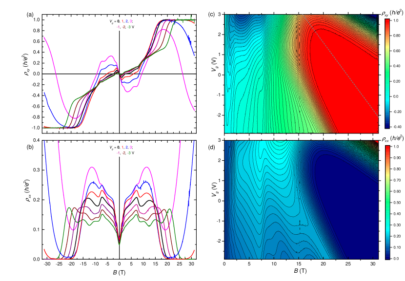
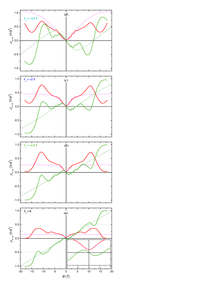
The samples are grown on a (013)-oriented GaAs substrate with their active part consisting of two HgTe layers, 20 nm wide, separated by a nm Cd0.65Hg0.35Te barrier. The DQW is symmetrically doped with In in the adjacent outer barriers at the distances of 10 nm from the outer interfaces. Here we outline the results for two samples, which are representatives of two investigated groups differed mainly by the hole densities . The first one (Sample 1) having a moderate m-2 at and the other (Sample 2) with a larger amount of Hg vacancies resulted in estimated larger m-2. The samples are shaped in the double Hall bridge and covered with a gate above the silicon insulating layer, as in Ref. Raichev-2012, . The results on the DQW are compared with those obtained on a single QW with identical parameters grown in the same technological cycle (20 nm wide, the same symmetrically doped). Diagonal and Hall magnetoresistances (MR), and , were measured simultaneously by the direct current reversal technique using an improved version of original experimental setup Suslov on a dc current of A under magnetic fields up to 31 T at a temperature of 0.31 K at a fixed or sweeping : Figs. 1, 2. In the latter case a continuous sequence of bipolar triangular or sawtooth pulses was applied to the gate with amplitudes corresponding to the predetermined range of at a frequency an order of magnitude smaller than the measuring rate at a sufficiently low field sweep. Based on these data, and were built as continuous functions of two variables: see Figs. 2(c,d).
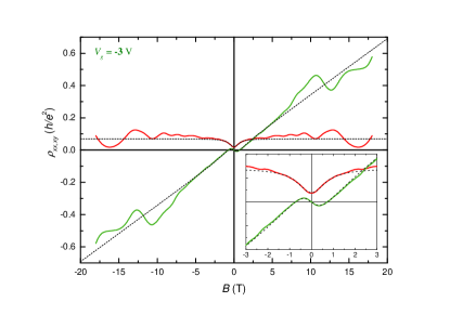
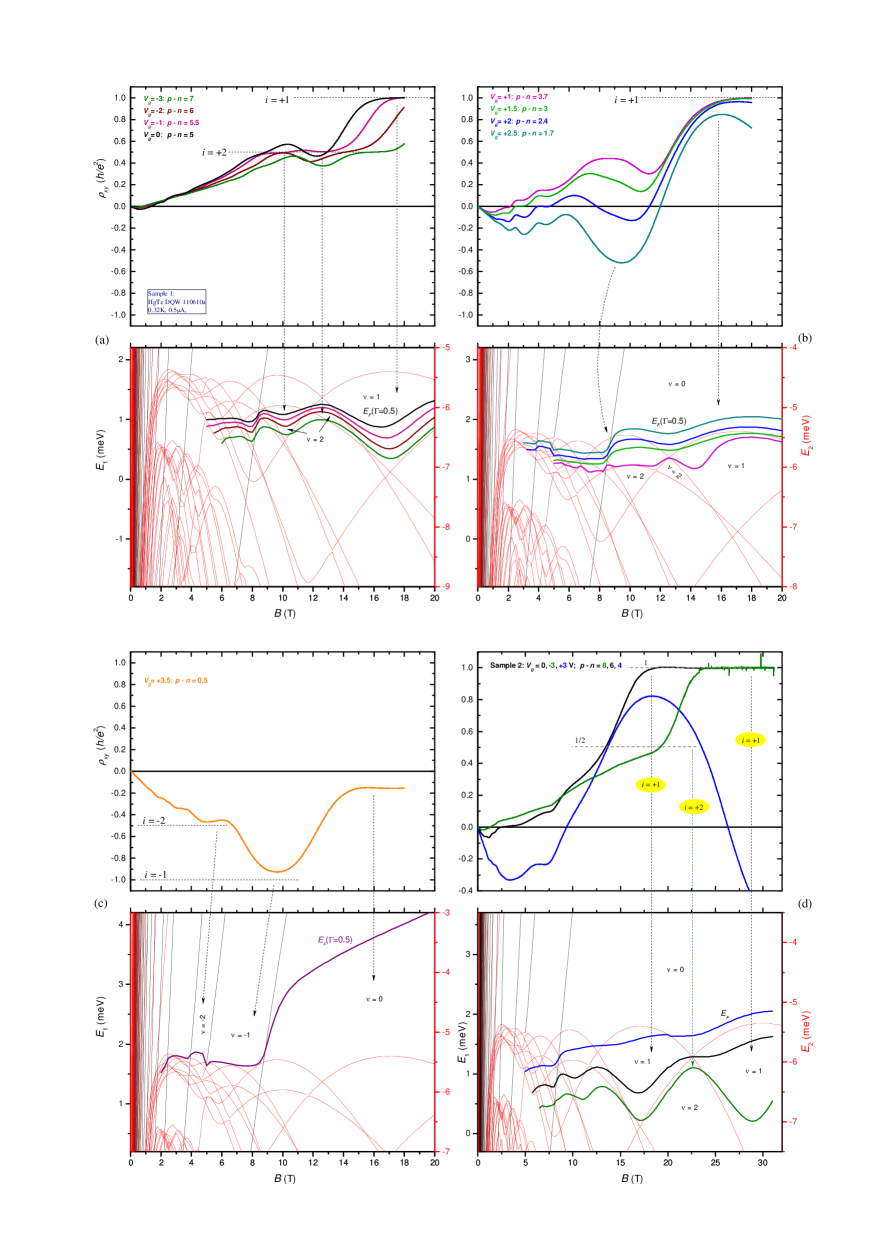
The curves for and at weak fields for negative and small positive voltages V +1 V have a structure relevant to the classical model of two kinds of free charges – a small quantity of high mobility electrons and a large quantity of low mobility holes, i.e., the N-shaped and a concomitant parabolic (Figs. 1, 2), as it was first found in Ref. Kvon JETPLett2008, for this heterosystem. MR oscillations are superimposed on this classical background. Within this range of , the positive reaches the quantum Hall (QH) plateau at for the hole component of conductivity in the highest fields simultaneously with dropping to zero. Also some feature exists in at representing a distorted QH state of holes.
There is a striking difference in the evolution of with within the QH range of fields for negative and small positive on one side and for the large on the other. The QH features in the hole conductivity component move in field linearly with in the former case as it should be for a regular picture of magnetic levels and a constant capacitance between the gate and the two-dimensional conducting system. To illustrate this linear dependence the dashed inclined line is drawn through the middle of the QH plateau area for Sample 2 in Fig. 2(c). Also such a linear shift is seen for the to plateau-plateau transition (PPT) in for both samples in Figs. 1(a) and 2(a). But more complicated behavior shows up for the further increase of . Instead of further shrinkage of the field scale as is expected in a simple case for the decreasing , we observe that the mentioned PPT stops moving to weaker fields at T and gradually sinks to negative values, passing through the states where several sign reversal points of exist (Fig. 1). Simultaneously the minimum at the highest fields moves up from zero. This behavior is quite different from that observed in a single QW where the transition from a positive to negative of an almost undistorted QH shape occurs rather sharply (see, e.g., Ref. Konig-2007Science, for a narrow QW and Ref. Minkov-2013, for a 20 nm wide well).
III Discussion of the results
The described behavior may be explained on a simplified scheme of magnetic levels as resulted from a superposition of the fan chart of electron levels upon the hole levels: Fig. 3. Indeed, when at large enough (corresponding to our case of negative ) is sufficiently deep in the valence subband, the superposed electron levels are empty, as if they are absent at all, and we have only a regular fan chart of the populated hole magnetic levels. In this case QH features would move linearly with decreasing and consequently – with increasing . We modeled a finite width of the levels by introducing a tentative Lorentzian density of states. Using Gaussian or semi-elliptic shape would not radically change the results. A QH feature in this picture corresponds to the range of fields where is sufficiently distant from both the neighboring levels when it passes through the gap between them. Introducing the finite level width makes it possible to display the finite sises of the QH features, but the main thing is that these calculations allow to represent automatically the behavior of when the electron levels come into play with the hole level. In the picture of overlapping hole and electron levels, a hole level is populated by free holes above simultaneously with free electrons occupying the electron level below (Fig. 3, inset).
When, on decreasing , the comes into touch with an electron level and this level starts to populate with free electrons, the corresponding QH feature stops moving towards lower fields. To elucidate this behavior the curves calculated for the full set of levels (solid lines in Fig. 3) are compared with those calculated for the same values of but for the case as if there are no electron levels: , dotted lines. It is seen that population of electron levels considerably modifies the positions of QH features stopping them in a vicinity of the point where the corresponding hole level crosses with an electron level. When , on moving along a hole level with decreased field, reaches the crossing electron level, then a part of electrons occupying the hole level below starts to move into the electron level (Fig. 3, inset) so that appears and increases. That is why, at fixed , increases and the corresponding QH feature within a set of hole levels appears at the fields higher than the position where it would be without the electron level. This process hampers the further shift of QH features with increasing to lower fields within a set of hole levels. Thus the experimental field where the QH features stop moving with indicates the approximate position of some crossing point in the picture of levels. Another important consequence appearing when approaches the electron level is an increased contribution of electron states into the magnetotransport that would manifest in a development of to negative values.
The reentrant sign-alternating behavior of has been revealed in a single HgTe QW in Ref. Raichev-2012, at much lower fields of several Tesla, and a value of the band overlap in their sample was estimated as of the order of 1 meV. Much higher fields of the sign reversal in our DQW structures indicate much larger overlaps and much higher values of characteristic fields for the level crossings.
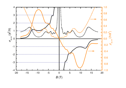
For the largest , of Sample 1 becomes fully negative and reveals a series of QH plateaus at intermediate fields due to electron conductivity component. However turns back towards zero at the highest fields [Fig. 1(a,c)] reaching a plateau-like feature close to zero. To emphasize the difference of this anomalous behavior of in the DQW from the traditional one, the trace for a single -type HgTe QW (measured without a gate) is added to Figs. 1(a,c). Concomitantly with the drop of in a DQW, a sharp growth appears in contrary to the behavior in the traditional QH effect (QHE). This quasi-zero plateau in is well reproduced in the conductivity (Fig. 4) and may be an indication of a zero-filling-factor state.Gusev-2010 We don’t see the electron QHE and its further development in Sample 2 because of a smaller achievable V due to a less reliable insulator under the gate in it. Nevertheless the reentrant sign change of combined with the sharp growth of are well seen in Fig. 2 at maximal fields and the maximum positive .
In the range of the largest , when a considerable electron part of is formed up to intermediate fields, remarkable is that the weak field slope of this curve does not change with , contrary to the data for single QWsKonig-2007Science ; Minkov-2013 where the increase of free charge density with manifests in a monotonic decrease of its slope, i.e., in a monotonic decrease of the Hall voltage.
III.1 Classical treatment
To estimate the parameters of free charges in our structures we first used a simple classical model for magnetotransport with two kinds of carriers (see, e.g., Ref. Seeger, ) – electrons with density and mobility and holes with density and mobility :
| (1a) | |||
| (1b) |
To extract these four parameters the following four quantitative experimental features in and were used: (i) a zero field resistivity ; (ii) a slope of the Hall resistivity at high fields where it should approach the value in the classical model; (iii) a slope of the Hall resistivity around zero and (iv) a field of the first inversion . Then a system of four equations for four unknowns reads:
| (2a) | |||
| (2b) | |||
| (2c) | |||
| (2d) |
which was solved numerically.
The classical description should be valid at weak fields while deviations from it may appear at higher fields caused by unconsidered complications due to quantization. This fit indeed works in our samples at the negative . Thus, for Sample 1, the weak field fit is excellent for V (Fig. 5) with m-2, m2/Vs, m-2, m2/Vs, while at higher fields the Shubnikov - de Haas oscillations (SHO) are superposed on the classical horizontal line for and a deviation from the inclined line for appears around the quantum Hall value of . The fits look reliable till around [Fig. 6(a)], where the obtained set is: m-2, m2/Vs, m-2, m2/Vs. As seen from these and further estimations the changes in MR with increasing are mainly connected here with the drop in the hole density while the changes in are not substantial and limited within the range of m-2 for the whole set of negative and positive . The weakness of the electron density dependence on is well seen for large V where the weak field part of shows a monotonous linear behavior due to a single kind of carriers – electrons only: , with the slope almost independent on (Fig. 1).
With a further increase of some factors of uncertainty appear in the overall MR. The first warning is that the QH features shift below the fundamental values of , initially for the distorted feature at for V [Figs. 6(a,b)], then for the plateau with for V [Figs. 6(c,d)]. The development of this tendency leads to appearing additional inversion points in : Fig. 6(c) for V and, with the further lowering of , for V [Fig. 6(d)] and V (Fig. 1). The nature of these inversion points is certainly different from the discussed above so that using them as a fitting point becomes problematic. Another characteristic feature used in fitting – a linear slope in at high classic fields – disappears at large . Thus, description by the classical two-carrier model becomes doubtful in this range of . The origin of these transformations may be in the admixture of additional electron states to the states of the hole magnetic levels as in speculations around Fig. 3.
A guess to explain this complicated behavior in classical terms is that it is a manifestation of an additional kind of particles with lower mobility. Their nature may be connected with the complicated structure of the valence subband top where an electron-like curvature of exists in some range of wave vector values around zero between the lateral maxima. These particles should behave like heavy electrons as the curvature is lower here than in the conduction subband. The addition of low mobility electron component to conductivity will cause a modification of Equations (1) into Equations (3), obtained by the reversal of conductivity tensor into the resistivity tensor:
| (3a) | |||
| (3b) |
with

Using Egs. (3) it is indeed possible to obtain a second reversal of (Fig. 7) for a realistic set of parameters: m-2, m2/Vs, m-2, m2/Vs, m-2, m2/Vs (, , and are the densities and the mobilities of two kinds of electrons). Of course, these values are less reliable than in case of a single inversion as here are 6 fitting parameters and the overall fitting is used within a range of weak fields. Thus this approach is rather an illustration of possible manifestation of heavy electrons. The next inversion of to positive values in Fig. 7 cannot be modeled in the three-carrier fit. A second kind of heavy holes with a still larger mass is needed for this. Thus, the task will be transformed into a four-carrier model. The necessity to add extra holes is seen from that is positive at the highest fields thus indicating that the sum of the hole densities is larger than that for the electrons, contrary to the presented values obtained in the three carrier fit. A nature of the second kind of holes may be suggested as being due to an asymmetry of the lateral maxima in the valence subband thus causing different values of on its opposite slopes. Some asymmetry in the DQW potential profile will lead to that different parts of the valence subband top would participate in the magnetotransport in the two layers thus providing heavy electrons from one layer and the second type of holes from the other one. We did not perform a four-carrier fit because of complexities and unreliable values expected for the 8 variable fit, but qualitatively the situation seems feasible once the classical approach works.
III.2 Oscillations in
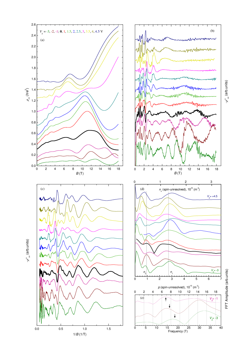
The uncertainty in obtaining parameters of free charge carriers from the classical magnetotransport at is a motivation to look for other ways to find them. Experimental curves for contain reach pictures of oscillations, although masked by the large and nonmonotonous backgrounds: Figs. 1, 2 and 8 (a). We extract the oscillations by taking their second derivative , Fig. 8 (b), that considerably enhances fast oscillations in the weak field region. Oscillations demonstrate several periods in reciprocal magnetic fields, , Fig. 8 (c), that is expectable for several populated subbands. To do the analysis feasible, considering weak initial amplitudes and a limited number of oscillations, we performed separate Fast Fourier Transformations (FFT) in the regions of high fields, where the high density holes manifest themselves in the high field oscillations for the negative , and within a low field window, where the oscillations should be due to the low density electrons: Fig. 8 (d, e). The upper axis is added for the electron and hole densities related to the FFT frequency as for the unresolved spin splittings.
In the low frequency range the FFT curves reveal two main peaks: one around m-2 and the other at m-2 as depicted by two dashed verticals in Fig. 8 (d). No directed movement of these peaks with is seen. In the high frequency window [Fig. 8 (e)] FFT peaks are revealed for the set of between V and V. One peak is close in its positions to the hole densities found from the two-carrier fits (indicated by arrows), if evaluations are performed for the spin unresolved case as . The second peak seen in Fig. 8 (e) at approximately double frequencies should be connected with the spin resolved component of the same oscillations and yields the same values if estimated for the spin resolved case as . The stable directed shift of the hole FFT amplitudes is seen with the changes of to negative values.
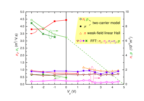
The results of all estimations for all kinds of carriers are collected in Fig. 9: for two-carrier fits that yield summary densities for electrons and holes and their mobilities for ; for simple weak-field classical linear yielding at maximum positive and for Fourier treatment of oscillations. When compared FFT results for electrons and the estimates for from the two-carrier fit it should be considered that in a latter case the fit would not feel the possible distribution of electrons between two subbands if they have comparable mobilities in the subbands, while FFT feels the difference in their densities. Then the sum obtained from FFT should be compared with obtained from two-carrier fit. As seen from Fig. 9 the dots for are between the data for two-carrier fits and simple classical linear weak-field in a reasonable agreement. The general conclusion about electrons is that is almost independent on .
We have reliable data on only for both for two-carrier fits and FFT analysis. However we can add one supplementary estimation for the positive . The Hall MR in its evolution with increasing becomes fully negative at V: Fig. 1. It should happen when exceeds . Thus, we can add this CNP to the function : at V. The dashed line in Fig. 9 depicts this rough prolongation of to the positive . The general conclusion on : it pronouncedly decreases with from m-2 at V to zero at about V.
III.3 Analysis based on the energy band calculations
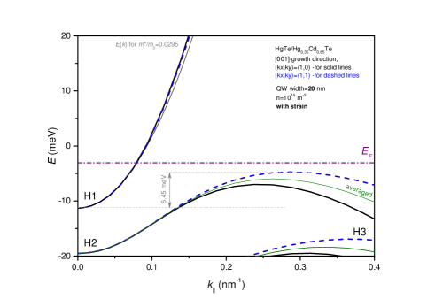
The energy band structure of a single fully strained QW, of which our DQW is built, was calculated in an envelope function approach within the framework of 8-band theory self-consistently with the Poisson equation for the charge distribution.ENovik We used the simple [001] orientation for calculations in spite of [013] growth direction in our structures hoping that the deviation between these directions would not influence considerably the results of our analysis, which is mainly of qualitative character. The resultant band structure is presented in Fig. 10.
In the valence subband, substantially differs for the (1,0) and (1,1) directions in the plain (bold solid and dashed curves in Fig. 10 respectively), so that the constant energy contours are warped. We ignored this warping in our rough estimations of the carrier densities and used the averaged curve for the valence subband dispersion (thin green curves in Fig. 10).
A substantial overlap about 6.5 meV of the valence and conduction subbands is obtained when the strain is considered in calculations (while the overlap is absent at all without strain). But this overlap would not be felt experimentally in a single QW at electron densities m-2 since the Fermi level is above the overlap region. Thus, attempts to use this picture without any modifications for interpretation of our experiments on DQWs would not be successful as we have m-2.
Calculations of the energy spectra for HgTe/CdHgTe DQWMichetti-Novik2012-2014 show that the tunneling gap between the states is vanishingly small. In this case the DQW energy spectrum may be obtained by a simple superposition of pictures calculated for single QWs composing the DQW, with a relative shift in energy if some electric field presents across the structure. Here remarkable is that we observe the QH plateau with in the DQW even for zero gate voltage. For zero tunneling gap the QH state is impossible in a DQW with symmetric potential profile. In this case the QH plateaus in each of the composing equal single QWs would yield the resulting Hall resistivity of the whole structure twice as smaller as for each layer switched in parallel thus corresponding to in the measurements on the DQW sample. In other words, the equal QWs would have equal sets of magnetic levels and combining these layers into a DQW structure of symmetric potential profile would simply lead to the doubling of all levels for zero tunneling gap. Thus the only possibility for appearing the gaps with odd filling factors in this case is an energy shift between the two layers. The existence of such a shift at may be due to asymmetric distribution of fixed charges: ionized dopants and uncontrolled impurities, surface charges, etc., or due to some differences in the shape of QWs.
III.3.1 Free charges distributions between subbands
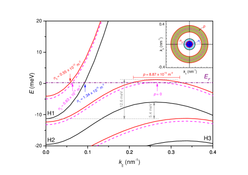
We can reconstruct the energy spectrum of our DQW and its evolution with using the data on the free charges in the subbands. First, we take an energy spectrum calculated for a single QW and determine where the Fermi level should be drawn in this picture to get the experimentally obtained . E.g., for m-2 measured at V, we calculate the area occupied by holes in the two-dimensional -space using the relation for the spin-degenerated states and adjust the position with respect to the lateral maxima of the valence subband to get this area of the ring cut from it by : see the solid red upper valence subband in Fig. 11 with the obtained position and the corresponding ring in the inset. The derived cuts a part of the conduction subband of this layer (see again the solid red upper curve but for the conduction subband), and a similar calculation yields m-2. This value is less than the measured m-2. The missing part of electrons is in the conduction subband of the other (lower) layer of the DQW: m-2. To fulfill this condition the energy spectrum of the lower layer is superposed onto that of the upper layer (black lower curves in Fig. 11) with a shift down on the energy of 7.2 meV that yields the area cut by from the conduction subband of the lower layer for the needed value of . Thus the value of the energy shift between the layers is determined. This superposition results in an increased overlap between the conduction and valence subbands from 5.4 meV within a single layer to 12.6 meV between the layers at the expense of inclusion of the interlayer overlap. The overlapped states of the two layers contribute to the common conductivity of the DQW, also the interlayer Coulomb interactions between them may result in a formation of the interlayer electron-hole correlated states and other processes.
Variation of causes a shift of the upper layer energy with respect to the lower layer energy while the latter is insensitive to as the lower layer is screened from the upper gate by the free charges in the upper layer. The upper layer energy also shifts with respect to , which is thus fixed in the lower layer and the part of the structure below. As we obtained experimentally, the increase of to positive values causes a drop of from a substantial value to zero while remains almost unchanged. The found DQW spectrum (Fig. 11) allows to explain this behavior. (i) The main part of the total electron density is in the lower layer conduction subband (), which is insensitive to . (ii) A very large density of states corresponds to the holes around the lateral maxima. These holes occupy a ring (a warped ring, to be more exact) in the 2D -space with an area an order of magnitude larger than for circle areas corresponding to electrons: Fig. 11(inset). A large effective mass corresponds to these holes. That is why a small decrease in the valence subband position with respect to causes a large drop in . So, for the drop from m-2 (at V) to zero (expected at V) only a lowering of the upper layer energy on 0.9 meV is needed: see the dashed pink curves in Fig. 11. This shift causes only a small increase of the electron density in the conduction subband of the upper layer, from m-2 to m-2, that amounts only about of the total increase in , on the background of large . This is also illustrated in the inset to Fig. 11 for the same shift: while the occupied valence subband ring shrinks into a pink dashed circle line with the lowering of the upper layer energy, the conduction circle for bordered with the red solid circle line expands only a little to the pink dashed circle contour whereas the black circle contour for remains unchanged.
This interpretation confirms the existence of two components in the electron conductivity seen in the Fourier spectra of oscillations where two FFT peaks for and were obtained: Fig. 8(d). The DQW spectrum presented in Fig. 11 explains why the QH state exists in DQW: the valence subband of the lower layer is shifted much below in the whole range of . Thus, it is always empty of holes and don’t contribute to the hole component of the QHE.
Why did we choose a scheme with the energy of the upper layer shifted above the energy of the lower layer? It is due to the observed dynamics of magnetotransport pictures with . In the opposite case (swap the colors in Fig. 11 between the red tint and the black) will be independent of as it will be in the valence subband of the lower layer and all the changes with increasing should be at the expense of large shifts down of the upper layer conduction subband energy, i.e., for the large increase in and of the total electron density , that is in drastic contrast with all our experimental data.
III.3.2 Peculiarities in the QH range of fields
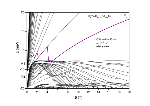
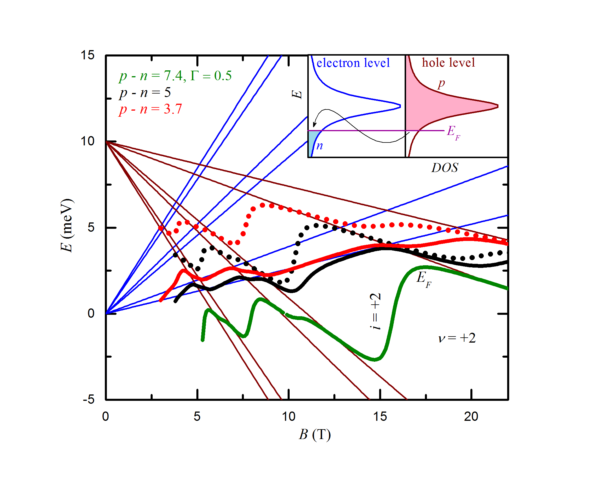
The scheme for computing was developed further for calculations of magnetic levels.ENovik The magnetic level picture for the spectrum presented in Fig. 10 is demonstrated in Fig. 12. Here an example of the Fermi level dynamics for m-2 is shown for the simplest case of -shaped density of states in the levels. It is noteworthy that while does not touch the valence subband in for this (Fig. 10) it nevertheless enters the set of valence magnetic levels between 4 and 5 T in Fig. 12. This may be connected with the anomalous nature of the lowest electron magnetic level. It is a so called zero-mode level, it starts from the valence subband at but monotonously moves up with field, as it should be for an electron level, while all the other valence subband levels, also starting from the valence subband at and moving initially like electron levels, turn down later at a certain field as they reach the energy of the lateral maximum thus behaving further like the hole levels. A nonmonotonous behavior of the main set of the valence subband levels is well understood from a quasiclassical view for the valence subband with the lateral maxima, but the anomalous behavior of the zero-mode level does not have a quasiclassical interpretation. We believe that this zero-mode level yields a negative contribution to the Hall voltage thus proving its electron character. Another zero-mode level, but of the hole nature, is seen in Fig. 12: it starts at from the conduction subband but monotonously moves down as it should be for the hole level. Being the hole level it should not contribute to the conductivity as it should be empty of holes when is above it. In fact the movement of is more complicated within the levels of finite width especially within the field ranges where the electron and hole levels overlap, according to the modeled picture of levels in Fig. 3.
The magnetic level pattern for the DQW is obtained similarly as it was done for the DQW energy spectrum in Fig. 11: the chart of levels calculated for the single QW in Fig. 12 is superimposed onto the same chart with the energy shift on the already known value of 7.2 meV. We used the so obtained diagram of DQW levels for interpretation of the observed features in the QH range of fields. Of course, this interpretation is far from to be exact, but we hope at least to understand some of the main trends. The Fermi level dynamics within the obtained plot of the DQW magnetic levels was calculated for the finite width Lorentzian shaped density of states in the levels similarly to that in Fig. 3. In these schematic calculations the levels in the valence subband were assumed to be of the hole nature within the whole range of fields (in spite of their electron-like behavior at low fields), i.e., their contribution to was programmed as positive, with exception of the zero-mode level, which was programmed as electron level as well as nonanomalous levels in the conduction subband. More detailed consideration of the nature of states in the levels is left for the future. The results of our calculations are presented in Fig. 13 for different free charge densities corresponding to the values of in experiment and compared to the measured .
The QH plateau observed at corresponds to the position of inside the triangle-shaped gap formed by the arc-shaped course of a level near the lateral maximum at the top and the positively and negatively sloped levels on its flanks: Fig. 13(a). The field when passes through the middle of the gap in this triangle correlates with QH plateau on . With decrease of the tendency is seen as the calculated values move to the higher fields in agreement with our experiment. The transition region between QH states for and corresponds to the left flank of the triangle. The movement of the PPT to higher fields with decreased correlates with the shifts of the point where intersects the left flank.
The gap for filling factor to the left from the triangular gap is formed by two negatively sloped and one positively sloped levels. It differs from the gap in shape and is much narrower. passes through this gap in the vicinity of three points where the levels cross. Existence of groups of closely spaced levels was observed to cause a similar distortion of the QH plateau in the shape of a dip (e.g., in a traditional DQWY2008 ; Y2009 ). A possible cause for appearance of such a dip on the QH plateau may be connected with an interplay between current carrying strips at the sample edges,Siddiki2014 and close positions of the neighboring levels may promote the effect.
With increase of the hole density decreases and the calculated Fermi level shifts upwards, finally penetrating into a gap above the lateral valence subband maxima and below the lowest electron level: Fig. 13(b,c). In the joint picture of the hole and electron levels, population of the hole levels is described by the positive filling factors: and population of the electron levels – by the negative ones: . Then the gap above the valence subband lateral maxima is formally designated by . It is characterized by an interference of the hole and electron states resulting in a drop of to zero in the vicinity of CNP. Simultaneously diverges: Figs. 1 and 2, as it was observed in a single HgTe QW at much smaller fields in the localRaichev-2012 and nonlocalGusev-2012 transport. Possible physics causing a sharp drop of to zero with simultaneous growth of may be connected with a formation of the interlayer electron-hole excitonsOlshanetskyJETPL2013 causing specific ratios for scattering probabilities between different channels.Raichev-2012
on passing with increased through the valence subband edge at intermediate fields goes repeatedly across the field regions where it is either below or above the hole magnetic levels: Fig. 13(b,c). This is due to the oscillating profile of the valence subband top formed in quantized magnetic fields by nonmonotonous course of the hole levels with different numbers around the energy of lateral maximum. Because of that and the superimposed electron levels the balance of the states on having the hole or electron character is alternatively changed. The contribution of electron states is enhanced when goes along the electron level between 8 and 9 T. All this results in several inversions in the course of .
Speculations developed on the modeled level picture presented in Fig. 3 that the movement of the hole QH features with is stopped when reaches a crossing point between the hole and electron levels may be justified in the pictures of the calculated levels shown in Fig. 13. Here the first stopping point is the crossing between two valence subband levels around T (the left corner of the actual triangular gap), which appears due to that the hole level behaves in an electron manner to the left from the field where it reaches the lateral maximum. This crossing point is responsible for the stop of moving in field of the PPT. Another actual crossing point also appears in the calculations (which is more in the spirit of the model in Fig. 3): the crossing of the lowest electron level with the valence subband edge between and 9 T. This point correlates with the minimum formed in around 10 T, which sinks to negative values at almost constant fields manifesting an increase in contribution of the electron states to magnetotransport at .
Similar behavior of quantum magnetotransport is observed at higher fields in Sample 2 (Fig. 13(d)). A distinct QH plateau at V (see also Fig. 2) correlates with location of inside the triangular gap for . The curve for V shows an inflection point at that correlates with the passage of within the gap, but closely to its upper edge, that is why this QH feature is weakly resolved. The plateau is rather wide for . It corresponds to the passage of through the two adjacent triangular gaps crossing the neck between them. Surprisingly this crossing is not reflected in the plateau shape. Probably there is some anticrossing within the neck that might smooth the expected feature. The feature is rather blurred here probable because the triangle gap is too narrow. goes out into the gap at high fields for V in agreement with the observed turn of to negative values. The oscillatory behavior of the valence subband edge is clearly manifested here as passes the positive gap close to its round top between T and 21 T resulting in a tendency for to reach the plateau and its further turn back to negative values at the weaker fields.
IV Conclusions
In summary, we have found that the inverted energy spectrum of the quasi-2D HgTe is substantially modified in the DQW structure built of these layers. The overlap of the conduction and valence subbands may be considerably increased in the DQW. Due to this fact the critical field for opening the gap in the energy spectrum shifts to much higher fields with respect to the critical field in a single QW. Thus, the accompanying specific features in magnetotransport, such as multiple inversions in , zero filling factor state with a concomitant manifestation of its insulator character in , etc., are moved to the range of higher fields where the QH regime is well realized. The effects of interlayer screening of the gate potential, which is never exhausted in the HgTe DQW, makes it possible to shift the energy spectra of the layers with respect to each other thus making possible to regulate the overlap between the conduction and valence subbands by the gate voltage . A huge difference in the density of states is found between the valence subband lateral maxima and the conduction subband minimum leading to that only the hole density is sensitive to while the electron density remains almost constant.
Acknowledgements.
Authors are grateful to E. Palm, T. Murphy, J. H. Park, and G. Jones for help with the experiment. The research was carried out within the state assignment of FASO of Russia (theme ’Spin’ No. 01201463330), supported in part by RFBR (project No. 14-02-00151) and the RAS Ural division complex program (project No 15-9-2-21). National High Magnetic Field Laboratory is supported by NSF Cooperative Agreement No. DMR-1157490 and the State of Florida.References
- (1) M. König, H. Buhmann, L. W. Molenkamp, T. Hughes, C-X. Liu, X-L. Qi, and S-C. Zhang, J. Phys. Soc. Jpn. 77, 031007 (2008).
- (2) Z. D. Kvon, E. B. Olshanetsky, D. A. Kozlov, N. N. Mikhailov, and S. A. Dvoretskii, JETP Letters 87, 502 (2008).
- (3) Z. D. Kvon, E. B. Olshanetsky, E. G. Novik, D. A. Kozlov, N. N. Mikhailov, I. O. Parm, and S. A. Dvoretsky, Phys. Rev. B 83, 193304 (2011).
- (4) E. B. Olshanetsky, Z. D. Kvon, N. N. Mikhailov, E. G. Novik, I. O. Parm, and S. A. Dvoretsky, Solid State Commun. 152, 265 (2012).
- (5) E. B. Olshanetsky, Z. D. Kvon, Ya. A. Gerasimenko, V. A. Prudkoglyad, V. M. Pudalov, N. N. Mikhailov, and S. A. Dvoretsky, JETP Lett. 98, 843 (2013).
- (6) M. V. Entin, L. I. Magarill, E. B. Olshanetsky, Z. D. Kvon, N. N. Mikhailov, and S. A. Dvoretsky, JETP 117, 933 (2013).
- (7) G. M. Gusev, E. B. Olshanetsky, Z. D. Kvon, N. N. Mikhailov, S. A. Dvoretsky, and J. C. Portal, Phys. Rev. Lett. 104, 166401 (2010).
- (8) O. E. Raichev, G. M. Gusev, E. B. Olshanetsky, Z. D. Kvon, N. N. Mikhailov, S. A. Dvoretsky, and J. C. Portal, Phys. Rev. B 86, 155320 (2012).
- (9) Y. Zhang, Z. Jiang, J. P. Small, M. S. Purewal, Y.-W. Tan, M. Fazlollahi, J. D. Chudow, J. A. Jaszczak, H. L. Stormer, and P. Kim, Phys. Rev. Lett. 96, 136806 (2006).
- (10) X. Ying, S. R. Parihar, H. C. Manoharan, and M. Shayegan, Phys. Rev. B 52, R11611 (1995); A. R. Hamilton, M. Y. Simmons, F. M. Bolton, N. K. Patel, I. S. Millard, J. T. Nicholls, D. A. Ritchie, and M. Pepper, Phys. Rev. B 54, R5259 (1996); R. Fletcher, M. Tsaousidou, T. Smith, P. T. Coleridge, Z. R. Wasilewski, and Y. Feng, Phys. Rev. B 71, 155310 (2005).
- (11) R. J. Nicholas, K. Takashina, M. Lakrimi, B. Kardynal, S. Khym, N. J. Mason, D. M. Symons, D. K. Maude, and J. C. Portal, Phys. Rev. Lett. 85, 2364 (2000).
- (12) K. Suzuki, S. Miyashita, and Y. Hirayama, Phys. Rev. B 67, 195319 (2003).
- (13) K. Suzuki, K. Takashina, S. Miyashita, and Y. Hirayama, Phys. Rev. Lett. 93, 016803 (2004).
- (14) G. M. Minkov, A. V. Germanenko, O. E. Rut, A. A. Sherstobitov, S. A. Dvoretski, and N. N. Mikhailov, Phys. Rev. B 88, 155306 (2013).
- (15) M. V. Yakunin, S. M. Podgornykh, N. N. Mikhailov and S. A. Dvoretsky, Physica E 42, 948 (2010).
- (16) M. V. Yakunin, A. V. Suslov, S. M. Podgornykh, S. A. Dvoretsky, and N. N. Mikhailov, Phys. Rev. B 85, 245321 (2012).
- (17) S. Girvin and A. H. MacDonald, in Perspectives in Quantum Hall Effect (NY: Wiley), Ch.5 (1997).
- (18) H. C. Manoharan, Y. W. Suen, M. B. Santos, and M. Shayegan, Phys. Rev. Lett. 77, 1813 (1996).
- (19) P. Giudici, K. Muraki, N. Kumada, Y. Hirayama, and T. Fujisawa, Phys. Rev. Lett. 100, 106803 (2008).
- (20) P. Michetti, J. C. Budich, E. G. Novik, and P. Recher, Phys. Rev. B 85, 125309 (2012); P. Michetti and B. Trauzettel, Appl. Phys. Lett. 102, 063503 (2013); J. C. Budich, B. Trauzettel, P. Michetti, Phys. Rev. Lett. 112, 146405 (2014).
- (21) A. V. Suslov, Rev. Sci. Instrum. 81, 075111 (2010).
- (22) M. König, S. Wiedmann, C. Brüne, A. Roth, H. Buhmann, L. W. Molenkamp, X.-L. Qi, and S-C. Zhang, Science 318, 766 (2007).
- (23) K. Seeger, Semiconductor Physics, An Introduction, 5-th ed. (Springer, Berlin, 1977).
- (24) E. G. Novik, A. Pfeuffer-Jeschke, T. Jungwirth, V. Latussek, C. R. Becker, G. Landwehr, H. Buhmann, and L. W. Molenkamp, Phys. Rev. B 72, 035321 (2005).
- (25) M. V. Yakunin, G. Galistu, and A. de Visser, Physica E 40, 1451 (2008).
- (26) M. V. Yakunin, A. de Visser, G. Galistu, S. M. Podgornykh, Yu. G. Sadofyev, N. G. Shelushinina, and G. I. Harus, J. Phys.: Conf. Ser. 150, 022100 (2009).
- (27) S. E. Gulebaglan, S. B. Kalkan, S. Sirt, E. M. Kendirlik, and A. Siddiki, Eur. Phys. J. B 87: 72 (2014).
- (28) G. M. Gusev, E. B. Olshanetsky, Z. D. Kvon, A. D. Levin, N. N. Mikhailov, and S. A. Dvoretsky, Phys. Rev. Lett. 108, 226804 (2012).