Mapping an electron wave function by a local electron scattering probe
Abstract
A technique is developed which allows for the detailed mapping of the electronic wave function in two-dimensional electron gases with low-temperature mobilities up to . Thin (“delta”) layers of aluminium are placed into the regions where the electrons reside. This causes electron scattering which depends very locally on the amplitude of the electron wave function at the position of the Al -layer. By changing the distance of this layer from the interface we map the shape of the wave function perpendicular to the interface. Despite having a profound effect on the electron mobiliy, the -layers do not cause a widening of the quantum Hall plateaus.
I Introduction
The envelope wave function of localized electrons in semiconductors is determined by the laws of quantum-mechanics and electrostatics. Although the shape of determines many physical properties, its precise form is experimentally only accessible under very favourable conditions and with substantial effort, for example using an UHV-STM 2007Suzuki . In this work we utilize the extremely short interaction length of neutral impurities in high quality GaAs/AlGaAs heterostructures, synthesized by molecular beam epitaxy (MBE) to map out the square of the electron wave function perpendicular to the interface. This requires to place very thin (“delta”) layers of Al atoms at varying positions and measure the electron mobilities, from which the electron scattering rates are determined. These scattering rates reflect the amplitude of the wave function at the position of the -layer.
Electrons in two dimensional electron gases (2DEG) in heterostructures are free to propagate along the interface but are localized perpendicular to itIhnBook . The eigenstates and eigenenergies in the absence of a scattering potential are
| (1) |
where , , is the normalized wave function for the lowest energy transverse mode. The factor is a normalization, is the ground state eigenenergy and is the effective mass.
The function can be calculated self-consistently by combining the Schrödinger and the Poisson equation. This requires assumptions about the material parameters of the semiconductor structures, particularly the boundary conditions, band offsets at the interface and the incorporation of doping atoms. Several software packages are available for numerical solutions Nextnano ; 1999Rother ; Snyder , which however suffer for example from the lack of precise values for the band offsets2010Gerhardts . Consequently, while the theoretical model describing the wave function is well established, is typically obtained only approximately by means of simulation.
Neutral impurities, e.g. atoms like Al with the same outer electron shell as Ga, are known to have very short interaction lengths 1984Walukiewicz ; 2003Li , although details of the scattering mechanism have not yet been resolved. Adding -layers of Al to the GaAs in the region where the 2DEG resides should allow to test the amplitude of at the -layer position. This is done by analyzing the electron mobility .
To utilize the Al -layer as local scattering center, it is of paramount importance to reduce all other scattering processes as much as possible. These processes include scattering by charged ionized donors, phonons, interface roughness and background impurities (see e.g. 1984Walukiewicz ). The latter stem from residuals in the MBE chamber that are inevitably incorporated during the growth process.
The phonon scattering can be effectively removed by cooling the sample to low temperatures. The role of the ionized donors is minimized by large setback distances between doping and 2DEG, and the effect of interface roughness appears to be negligible under optimized growth conditions. The background impurities can only be reduced if the heterostructures are synthesized under extreme purity in specialized molecular beam epitaxy (MBE) setups. The “quality” of a given MBE setup is generally measured by the maximum electron mobility which has been achieved in quantum-well structures2002Arthur ; 2003Pfeiffer ; 2009Umansky ; 2010Schlom ; 2014Manfra . Mobilities exceeding (measured at ) have been achieved with the MBE setup used by us for growing the Al-doped samples2015DisIch .
II Experimental details
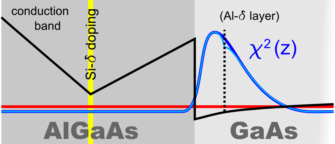
As the basic sample design we use single-sidedly doped heterostructures (Fig. 1) grown in the following sequence: We start with a superlattice consisting of periods of AlGaAs and GaAs. This is followed by GaAs hosting the 2DEG at the interface to an adjacent thick AlGaAs layer. This region contains a thin doping layer of silicon, placed at a setback distance of from the interface. The whole structure is capped by of GaAs. The Al content of the AlGaAs is throughout. These values are based on a growth rate calibration that is performed on a daily basis and secures that rates and with that layer thicknesses are precise within a margin of less than (see 2015DisIch for a detailled description). A series of different samples are grown containing Al impurities which replace the Ga atoms in the GaAs crystal structure. This is done by adding (one monolayer) AlGaAs and with that Al atoms to the GaAs at distances from the interface varying from to . The average distance between the Al atoms in this layer is . The dispersion of the AlGaAs delta layer due to migration during the growth process can be considered negligible. TEM analysis of structures produced under similar growth conditions shows sharp interfaces of an AlAs layers of width. The same is true for a buffer superlattice as described above. A TEM image of such a superlattice with comparable interface quality is shown in 2014Manfra .
Transport properties were measured by the van-der-Pauw technique, both in the dark and after illumination with a red () LED. Magnetotransport data were obtained at at magnetic fields up to Tesla. The electron densities and mobilities at of the sample without any Al impurities are and in the dark and and after illumination, respectively. This structure serves as the reference for the series with Al -layers at varying distances and will furtheron be referred to as .
III The scattering vs. Al-doping depth
| distance [] | density [] | mobility [] | scattering rate [] |
|---|---|---|---|
| 0 | 1.52 | 8.036 | 3.27 |
| 5 | 1.40 | 1.293 | 20.30 |
| 10 | 1.39 | 0.793 | 33.1 |
| 15 | 1.416 | 1.813 | 14.48 |
| 20 | 1.461 | 3.746 | 7.01 |
| 25 | 1.561 | 7.331 | 3.58 |
| 30 | 1.574 | 8.281 | 3.17 |
| distance [] | density [] | mobility [] | scattering rate [] |
|---|---|---|---|
| 0 | 1.98 | 13.75 | 1.91 |
| 5 | 1.79 | 1.98 | 13.255 |
| 10 | 1.76 | 1.14 | 22.98 |
| 15 | 1.81 | 2.309 | 11.37 |
| 20 | 1.96 | 5.21 | 5.04 |
| 25 | 1.99 | 9.53 | 2.75 |
| 30 | 2.04 | 12.77 | 2.05 |
The tables 1 and 2 summarize the results for measurements made in the dark and after illumination at , respectively. As usual, the illuminated structures have larger electron densities compared to those measured in the dark. Adding the Al -layers has a significant effect on electron mobility: drops by an order of magnitude from to after illumination, and from to in the dark), if the Al is placed away from the interface (which is the mobility range of what Gardner et al. reported for a comparable, homogeneously distributed amount of Al atoms 2013Gardner ). We note that we are able to reproduce the magnetotransport characteristics of nominally identical samples, originating from different growth runs within a margin of for electron density and for mobility2014ich .
It is useful to compare the transport scattering rates rather than the mobilities to discriminate the intrinsic scattering processes – caused by background impurities in the growth chamber, remote ionized donor potential disorder, interface roughness and phonon scattering – from the ones induced exclusively by the Al impurities. The total scattering rate should be the sum of the intrinsic rate and the one due to the Al impurities :
| (2) |
is calculated from the relation , where and are the elementary charge and the effective electron mass, respectively.
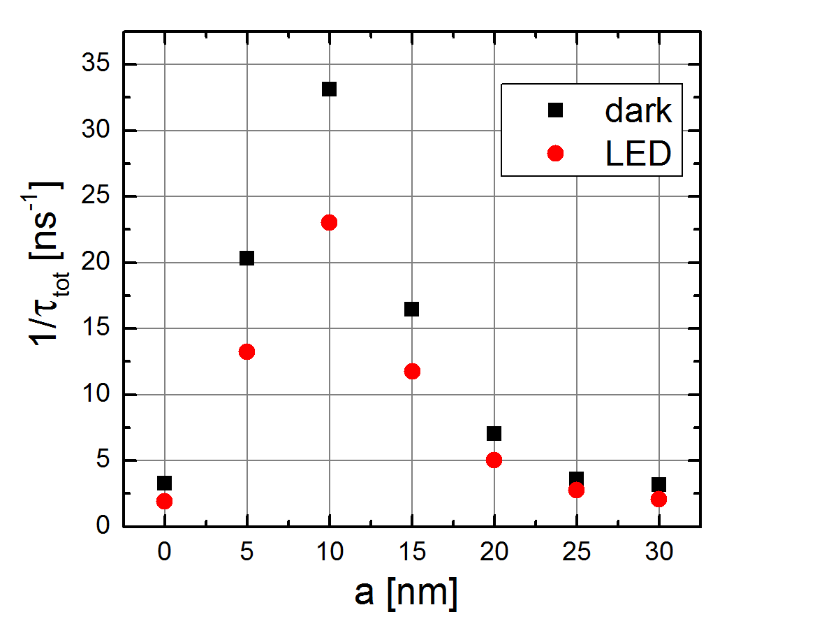
The resulting scattering rates are shown in tables 1 and 2 and are plotted in Fig. 2. Unexpectedly, the electron density is reduced by up to , if the Al -layer is located in the to range. This systematic change is too large to be accustomed to uncertainties in the growth process (those may account for a density variation of no more than ) or the error margin of the characterization.
The scattering rates have a maximum at a distance of from the interface where they exceed the reference values by a factor of about . It is noteworthy that not only the reference scattering rate but also the one due to the Al atoms decrease after illumination.
IV Scattering by neutral impurities – Theory
Although a first principle calculation of the scattering is difficult, a simple approximation can be obtained by modifying the approach used in 1976Harrison ; 1983Basu in such a way that the scattering sites now exist only in the Al -layer. In this approach one considers the Ga atoms being replaced by Al atoms randomly in some sites (possibly also clustering around these sites, such that are the centers of these clusters). The average () and the random () part of the potential are
| (3) |
where and are the approximate thickness and the position of the Al -layer, respectively, and each is a random variable which is with a probability of and with probability . Here is the Al concentration in the -layer. We assume that in different sites are uncorrelated so that the expectation value over the disorder realizations satisfies .
The homogeneous average potential does not cause scattering, so that the scattering rate is completely determined by the random potential . We parametrize the potential around each site as
| (4) |
where is the Heaviside step function, and and describe the magnitude and the range of the scattering potential caused by each cluster. The scattering rate can be calculated using Fermi’s golden rule
| (5) |
where is the angle between and and is the matrix element caused by the random alloy scattering potential. By assuming that the Fermi wavevector satisfies , we obtain
| (6) |
where is the number of scattering sites.
This formula shows that the scattering rate is proportional to the fourth power of the wave function at . This behavior is used for the wave function mapping. The dependence of the scattering rate on the fourth power of leads to the rapid variation of the scattering rates with the distance from the interface as seen in the data presented in Fig. 2.
For a quantitative estimate of the scattering rate one has to make assumptions about and the the scattering potential . We assume that the range and the spacing between the scattering sites are on the same order . Then the only free parameter is the magnitude of the scattering potential , which is expected to be on the order of eV corresponding to the conduction band variations if Al atoms are alloyed to the GaAs. With at (see Fig.3) and a we find a scattering rate which is very close to the numbers measured.
Although the value of deduced from this analysis is considerable smaller than the one found by Li et al. 2003Li for GaAs homogeneously doped with Al, we believe that this discrepancy arises mainly from model-specific assumptions that influence the value obtained for . In particular the parameters and have significant uncertainties due to the possible clustering of the atoms, and in this work we have made different assumptions for these parameters than in 2003Li . Despite these uncertainties in the relative magnitudes of the parameters, this theoretical calculation illustrates that the experimentally measured scattering rates are consistent with the alloy scattering mechanisms since quantitative agreement can be obtained with a reasonable choice of the parameters , and .
V Determining the wave-function shape
Based upon the data presented in Fig.2, we use equation 6 to deduce the shape of the squared envelope wave function . First, one needs to substract an estimate of ( and for the dark and illuminated state, respectively). The square root of the resulting is plotted as dots in Fig. 3(a) and (b) for the illuminated and the non-illuminated case respectively.
These data points can be compared with theoretically expected wave functions 111For this comparison between measurement and simulation data we use as a first order approximation wave function as obtained by simulation without the Al -layer. This appears to be a reasonable approximation, since including the Al layer into the simulation leads to a density variation of less than and a maximum change in of less than . of the 2DEGs, obtained from the 8-band Schrödinger-Poisson-solver software NextnanoNextnano which uses parameters from 2001Vurgaftman , including a conduction band offset of for an Al-fraction of . The simulated structure is identical to the actual samples, including a silicon doping layer with a density of . Since the simulation neglects the formation (and fraction) of DX-centers, the resulting wave function is only applicable to the illuminated case, when almost all DX-centers are ionized. The resulting wave function is shown as the dashed red curve in Fig. 3(a), its calculated electron density is higher () than what was observed experimentally (); however, its agreement with the experimental data is already very good and gives trust in the mapping technique used here.
The fit can even be improved by adjusting the density of active donors in the simulation to find a 2DEG density that matches the measured one. This approach leads to the red solid line in Fig. 3(a), which agrees excellently with the data points.
Fig. 3(b) plots the data obtained in the dark. Using the the procedure as in the illuminated case, including an adjustment in the active donor density (represented by the black solid line), leads to a less good agreement with the data, particularly on the wave function’s flank far from the interface. This hints that the 2DEG is more strongly confined than anticipated by the simulation software. Such an enhanced confinement could be the result of deep level p-type impurites gettered by the highly reactive aluminium in the AlGaAs/GaAs superlattice located far below the actual heterostructure. The dashed line in Fig. 3(b) exemplarily shows the resulting wave function for a background impurity density of in the AlGaAs buffer layers222Note that a background impurity density this high is assumed only for the inital stages of the growth run and might for example stem from the oxide layer protecting the substrate surface before growth. We further assume that the background impurity level is not constant during the growth run but is continuously reduced by gettering/pumping. A mobility-density analysis as described in 2010Mak was performed by the Ritchie group on a comparable structure grown by us and suggests a charged background impurity of in the 2DEG region. . Using this scenario, the experimentally observed wave function can be reproduced very well for the dark case also. By means of illumination, the background impurities in the buffer layers might be compensated, leading back to the situation described above for the illuminated case.
(a)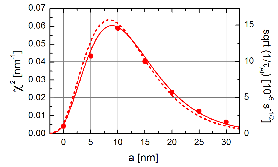
(b)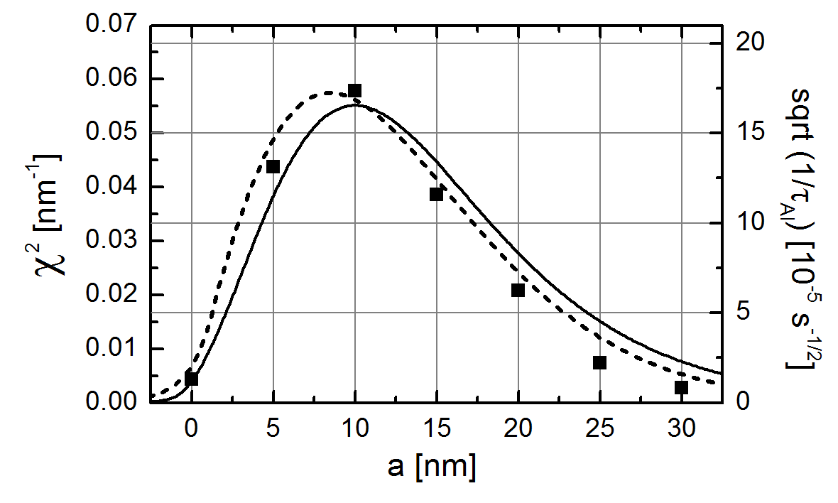
Overall, the agreement of the fit and the experimental data is surprisingly good, from which we conclude that the scattering potential of the Al atoms acts very locally on the electron wave function. It is noteworthy that not only the intrinsic scattering rates but also are reduced after illumination. The intrinsic scattering is probably due to charged impurities, both from the Si-doping and in the 2DEG region. In both cases screening has always been considered to be very effective. Our data indicate that for the scattering by neutral impurities, a density dependence exists, which also cannot be explained by the shift of the wave function due to the illumination. Such a dependency has, however, been neglected in previous theories1984Walukiewicz and is also not part of our analysis in section IV.
VI The effect on magnetotransport
In high perpendicular magnetic fields, the electronic transport properties show the integer quantum Hall effect (IQHE). Generally, the widths of the plateaus and the accompanying minima in the resistance depend on the density of localized states between the Landau levels 1981AOKI containing the extended states.
Increasing the scattering rate is therefore expected to increase the density of localized states at the expense of the extended ones and to lead to a widening of the SdH minima in the range of the IQHE plateaus. This behaviour is demonstrated by the trace corresponding to the sample “low ” (grey line in Fig. 4) which has been grown in an MBE system that was in a poor state at the time of growth, i.e. which contains a high number of residual charged and neutral impurities. It’s electron mobility of is similar to the one of the sample (represented by the red line). One might expect a similar widening of minima from samples with an Al -layer having a comparable mobility.
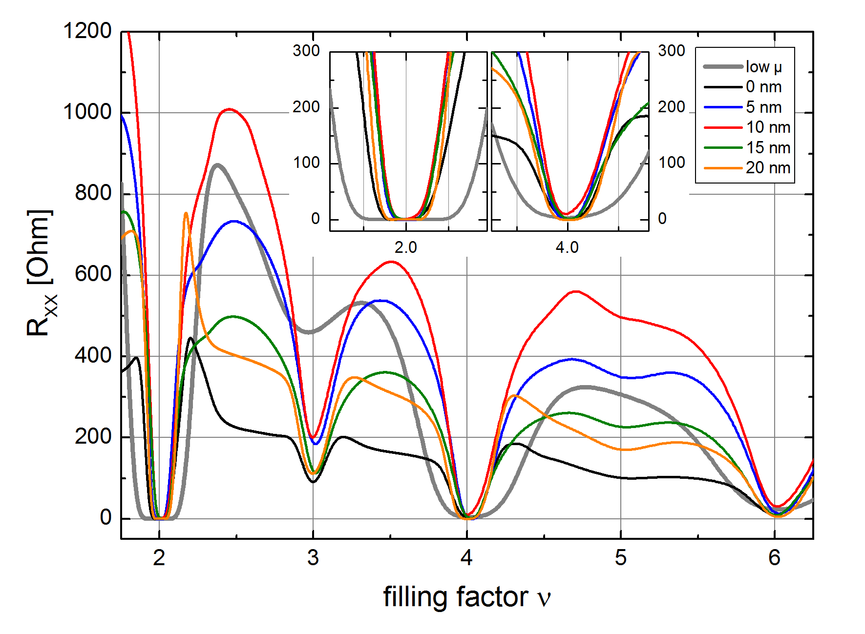
We have measured the magnetotransport characteristics at up to for our samples. The resulting longitudinal resistances as function of filling factor are shown in Fig. 4. Clearly, no significant widening of the minima at integer filling with the scattering rate is observed, although the scattering rates vary by a full order of magnitude. In contrast, the maxima between the integer filling increase considerably with the scattering rates.
The distance of the -layer from the interface seems to be more relevant for the shape of the curves in the regions between the integer fillings. It would be of interest to study this behaviour as function of (lower) temperature and compare the results with the scaling study of Li et al.2005Li . This is however beyond the scope of this work. It is noteworthy that also fractional quantum Hall effect gaps, measured by Deng et al. 2014aDeng , showed surprisingly little change from moderate but homogeneous Al doping which may be related to the lack of the localized-states background.
VII Conclusions
Placing -layers of Al impurities into GaAs in the regions of the 2DEG leads to substantially enhanced electron scattering rates. The dependence of these scattering rates precisely images the shape of the wave function , verifying that the scattering potential acts very locally on the electron wave function. This behavior makes this simple technique a unique way to map out the spatial distribution of 2DEG wave functions.
Although the scattering rate due to the Al atoms was enhanced by a factor of compared to the reference sample, it does not influence the width of the IQHE plateaus. This indicates that this scattering process does not contribute to the background of localized states between the Landau levels. The Al atoms do however enhance the resistance maxima between the integer filling factors. This indicates that the Al atoms cause a purely elastic scattering process. The missing of an increase of the localized background may also be relevant for the observation by Deng et al. that neutral background impurities – in the form of a homogeneous Al-doping – do not have a significant impact on the activation energy of the FQHS2014aDeng .
Using this technique it will be possible to map out wave functions of rectangular quantum wells which are of special interest for higher mobilities. Such structures are the testbed for investigations on the exotic = 5/2 state, whose quality is currently limited by the influence of remote ionized donors 2009Umansky ; 2013Muraki . Their effect would be minimal on a symmetric wave function. Currently such a symmetry can only be aimed at by calculating the required upper and lower doping density, but is very difficult to verify.
Furtheron, the technique can be used for wide quantum wells and double-quantum well systems. In such systems, the local electron density distribution develops two maxima that need to be balanced. Again, carefully placed Al -layers would be helpful as a sensor to optimize the growth parameters to achieve a balancing between two (partial) wave functions. We acknowledge stimulating discussions with Yongqing Li, Fabian Schläpfer and Lars Tiemann. The cooperation with Matthias Berl, Stefan Faelt, Jessica Gmür, Siegfried Heider, Marcel Sturzenegger was essential for operating the MBE system at the high quality level. We gratefully acknowledge the financial support of the Swiss National Foundation (Schweizerischer Nationalfonds, NCCR “Quantum Science and Technology”). This work was supported by the Academy of Finland through its Center of Excellence program, and by the European Research Council (Grant No. 240362-Heattronics).
References
- (1) K. Suzuki, K. Kanisawa, C. Janer, S. Perraud, K. Takashina, T. Fujiswa, and Y. Hirayama Phys. Rev. Lett. 98, 136802, Mar 2007.
- (2) T. Ihn, Semiconductor Nanostructures, Oxford, 2010.
- (3) S. Birner, “Nextnano, www.nextnano.de/.”
- (4) M. Rother, “Aquila, www.rotherland.de/de/aquila.htm.”
- (5) G. Snyder, “1dpoisson, www3.nd.edu/ gsnider/.”
- (6) R. R. Gerhardts Phys. Rev. B 81, 205324, May 2010 and private communication.
- (7) W. Walukiewicz, H. Ruda, J. Lagowski, and H. Gatos Phys. Rev. B 30, 4571, Oct 1984.
- (8) W. L. Li, G. A. Csathy, D. C. Tsui, L. N. Pfeiffer, and K. W. West Appl. Phys. Lett. 83, 2832–2834, Oct 2003.
- (9) J. R. Arthur Surf. Sci. 500, 189 – 217, Mar 2002.
- (10) L. Pfeiffer and K. W. West Physica E 20, 57, 2003.
- (11) V. Umansky, M. Heiblum, Y. Levinson, J. Smet, J. Nübler, and M. Dolev J. Cryst. Growth 311, 1658–1661, Mar 2009.
- (12) D. G. Schlom and L. N. Pfeiffer Nat. Mater. 9, 881–883, Nov 2010.
- (13) M. J. Manfra Ann. Rev. of Cond. Mat. Phys. 5, 347, 2014.
- (14) C. Reichl, MBE growth of ultrahigh-mobility 2DEG in GaAs/AlGaAs. Phd thesis, ETH Zurich, Jan 2015.
- (15) G. Gardner, J. Watson, S. Mondal, N. Deng, G. Csáthy, and M. Manfra Appl. Phys. Lett. 102, 252103, Jun 2013.
- (16) C. Reichl, J. Chen, S. Baer, C. Rössler, T. Ihn, K. Ensslin, W. Dietsche, and W. Wegscheider New J. Phys. 16, 023014, Feb 2014.
- (17) J. W. Harrison and J. R. Hauser Phys. Rev. B 13, 5347–5350, Jun 1976.
- (18) P. K. Basu and B. R. Nag Appl. Phys. Lett. 43(7), 689, 1983.
- (19) For this comparison between measurement and simulation data we use as a first order approximation wave function as obtained by simulation without the Al -layer. This appears to be a reasonable approximation, since including the Al layer into the simulation leads to a density variation of less than and a maximum change in of less than .
- (20) I. Vurgaftman and J. Meyer J. Appl. Phys. 89, 5815–5875, Jun 2001.
- (21) Note that a background impurity density this high is assumed only for the inital stages of the growth run and might for example stem from the oxide layer protecting the substrate surface before growth. We further assume that the background impurity level is not constant during the growth run but is continuously reduced by gettering/pumping. A mobility-density analysis as described in 2010Mak was performed by the Ritchie group on a comparable structure grown by us and suggests a charged background impurity of in the 2DEG region.
- (22) H. Aoki and T. Ando Solid State Commun. 38(11), 1079–1082, 1981.
- (23) W. L. Li, G. A. Csathy, D. C. Tsui, L. N. Pfeiffer, and K. W. West Phys. Rev. Lett. 94, 206807, May 2005.
- (24) N. Deng, G. C. Gardner, S. Mondal, E. Kleinbaum, M. J. Manfra, and G. A. Csathy Phys. Rev. Lett. 112, 116804, Mar 2014.
- (25) G. Gamez and K. Muraki Phys. Rev. B 88, 075308, Aug 2013.
- (26) W. Y. Mak, K. das Gupta, H. E. Beere, I. Farrer, F. Sfigakis, D. A. Ritchie Appl. Phys. Lett. 97, 242107, Dec 2010.