Terahertz ratchet effects in graphene with a lateral superlattice
Abstract
Experimental and theoretical studies on ratchet effects in graphene with a lateral superlattice excited by alternating electric fields of terahertz frequency range are presented. A lateral superlatice deposited on top of monolayer graphene is formed either by periodically repeated metal stripes having different widths and spacings or by inter-digitated comb-like dual-grating-gate (DGG) structures. We show that the ratchet photocurrent excited by terahertz radiation and sensitive to the radiation polarization state can be efficiently controlled by the back gate driving the system through the Dirac point as well as by the lateral asymmetry varied by applying unequal voltages to the DGG subgratings. The ratchet photocurrent includes the Seebeck thermoratchet effect as well as the effects of “linear” and “circular” ratchets, sensitive to the corresponding polarization of the driving electromagnetic force. The experimental data are analyzed for the electronic and plasmonic ratchets taking into account the calculated potential profile and the near field acting on carriers in graphene. We show that the photocurrent generation is based on a combined action of a spatially periodic in-plane potential and the spatially modulated light due to the near field effects of the light diffraction.
pacs:
68.65.Pq, 72.80.Vp, 65.80.CkI Introduction
Graphene has revealed fascinating phenomena in a number of experiments owing to specifics of the electron energy spectrum resembling that of a massless relativistic particle Review0 ; Review ; Review2 ; Review3 ; Review4 . Unique physical properties of graphene, such as the gapless linear energy spectrum, pure two-dimensional (2D) transport, strong plasmonic response, and comparatively high mobility at room temperature, open the prospect of high-speed electronics and optoelectronics, in particular, fast and sensitive detection of light for a range of frequencies from ultraviolet to terahertz (THz). Different mechanisms, by which the detection can be accomplished, include: (i) photoconductivity due to bolometric and photogating effects bolometer ; bolometer2 ; koppens , (ii) photo-thermoelectric (Seebeck) effect photothermo , (iii) separation of the photoinduced electron-hole pairs in a periodic structure with two different metals serving as contacts to graphene mueller ; weiss (double comb structures) or a - junction novoselov , and (iv) excitation of plasma waves in a gated graphene sheet plasmawave ; plasmawave2 , for reviews see Tredicucci14 ; Koppens14 ; kono14 ; knaprev2013 ; knaptredicuccirev2013 ; Boppel2012 ; Tonouchi2007 . As we show below graphene based detectors may operate applying ratchet effects excited by THz radiation in a 2D crystal superimposed by a lateral periodic metal structure. The ratchet effect is of very general nature: The spatially periodic, noncentrosymmetric systems being driven out of thermal equilibrium are able to transport particles even in the absence of an average macroscopic force reimann . This effect, so far demonstrated for semiconductor quantum wells with a lateral noncentrosymmetric superlattice structures Olbrich_PRL_09 ; Olbrich_PRB_11 ; Review_JETP_Lett ; popovAPL ; otsuji ; otsuji2 ; otsuji3 ; faltermeier15 , promises high responsivity, short response times, and even new functionalites, such as all-electric detection of the radiation polarization state including radiation helicity being so far realized applying photogalvanics helicitydetector ; ellipticitydetector . Most recently electronic and plasmonic ratchet effects have been considered theoretically in Ref. Theory_PRB_11 ; popov2013 ; Budkin2014 ; Koniakhin2014 ; Rozhansky2015 ; Popov2015 supporting the expected benefit of graphene based detectors.
In the present work, we report on the experimental realization and systematic study of graphene ratchets in both (i) epitaxially grown and (ii) exfoliated graphene with an asymmetric lateral periodic potential. The modulated potential has been obtained by fabrication of either a sequence of metal stripes on top of graphene or inter-digitated comb-like dual-grating-gate structures. We demonstrate that THz laser radiation shining on the modulated devices results in the excitation of a direct electric current being sensitive to the radiation’s polarization state. The application of different electrostatic potentials to the two different subgratings of the dual-grating-gate structure and variation of the back gate potential enables us to change in a controllable way the degree and the sign of the structure asymmetry as well as to analyze the photocurrent behaviour upon changing the carrier type and density. These data reveal that the photocurrent reflects the degree of asymmetry induced by different top gate potentials and even vanishes for a symmetric profile. Moreover, it is strongly enhanced in the vicinity of the Dirac point. The measurements together with a beam scan across the lateral structure prove that the observed photocurrent stems from the ratchet effect. The ratchet current consists of a few linearly independent contributions including the Seebeck thermoratchet effect as well as the “linear” and “circular” ratchets, sensitive to the corresponding polarization of the driving electromagnetic force. The results are analyzed in terms of the theory of ratchet effects in graphene structures with a lateral potential including the electronic and plasmonic mechanisms of a photocurrent in periodic structures. We show that the ratchet photocurrent appears due to the noncentrosymmetry of the periodic graphene structure unit cell. The experimental data and the theoretical model are discussed by taking the calculated potential profile and near-field effects explicitly into account.
II Samples and Methods
We study the ratchet photocurrents in two different types of structures. The superlattices of the first type are fabricated on large area graphene grown by high-temperature Si sublimation of semi-insulating SiC substrates Seyller1 ; Seyller2 . This type of sample with the superlattice covering an area of about mm2 on a graphene layer with a total area of about mm2 allowed us, on one hand, to scan the laser beam across the superlattice and, on the other hand, to examine the photocurrent in directions along and perpendicular to the metal stripes. All samples are made from the same wafer of SiC. To obtain defined graphene edges we removed an edge trim of about 200 m width, see Fig. 1(c), by reactive ion etching with an argon/oxygen plasma. The carrier mobility cm2/Vs and residual hole density 5.3 cm-2 in graphene resulting in a carrier transport relaxation time = 16 fs were measured at K. Before fabricating the superlattice structure, we carefully checked that the symmetry of the pristine graphene is unaffected by steps (terraces), which may be formed on the SiC surface. For that we studied the THz radiation induced photocurrent and ensured that it vanishes at normal incidence footnote0 ; Karch_PRL_2010 ; Glazov2014 . As a further step, we deposited an insulating aluminium oxide layer on top of the graphene sheet. For this purpose, we first deposited a thin ( nm) Al seed layer by evaporation in ultra high vacuum and oxidized it subsequently. Then we prepared 26 nm layer of aluminum oxide with atomic layer deposition using H2O and trimethyl aluminum as precursors. The lateral periodic electrostatic potential is created by micropatterned periodic grating-gate fingers fabricated by electron beam lithography and subsequent deposition of metal (5 nm Ti and 60 nm Au) on graphene covered by Al2O3. A sketch of the gate fingers and a corresponding optical micrograph are shown in Figs. 1(a) and (b), respectively. The grating-gate supercell consists of two metal stripes having different widths m and m separated by different spacings m and m. This supercell is repeated to generate an asymmetric periodic electrostatic potential Olbrich_PRB_11 ; staab2015 (period m) superimposed upon graphene, see Fig. 1(b). The mm2 area grating-gate structure is located on the left half of the sample so that a large graphene area remains unpatterned, see Fig. 1(c). For the THz beam of 1.5 mm diameter, this design allows us to study the photocurrent excited in either the superlattice structure or the unpatterned graphene reference area. Contact pads were placed in a way that the photo-induced currents can be measured parallel (, contacts 2 and 6) and perpendicular (, contacts 1 and 4) to the metal fingers. Two additional contacts (3 and 5) were used for detecting the photocurrent signals from the unpatterned area as a reference.
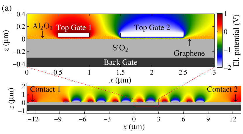
The structures of the second type are fabricated on small area graphene flakes Review0 . The benefit of these type of structures is the possibility to apply different bias voltages to the individual subgrating gates forming the superlattice allowing us to explore the role of the asymmetry of the lateral periodic electrostatic potential in the photocurrent formation as well as to examine the ratchet effects in the vicinity of the Dirac point. The graphene layers were prepared by mechanical exfoliation of natural graphite onto an oxidized silicon wafer. The samples used in this study were all single layer flakes. The periodic lateral electrostatic potential is created by 5 nm/60 nm Ti/Au inter-digitated metal-grating gates deposited on top of the graphene layer, see Fig. 1(d)-(f), applying the method described above. The insulating layer of aluminum oxide is used to separate the grating gates and graphene. The asymmetric lateral structure incorporates the inter-digitated dual-grating gates (DGG) TG1 and TG2 having different stripe width and stripe separation. An optical micrograph of the interdigitated grating-gates is shown in Fig. 1(e). The supercell of the grating gate fingers consists of metal stripes having two different widths m and m separated by spacings m and m, Fig. 1(d). This asymmetric supercell is repeated six times to create a periodic asymmetric potential (period m), Fig. 1(e). The two subgrating gates, each formed by fingers of identical width, can be biased independently. Therefore, the asymmetry of the lateral potential of the DGG structure can be varied in a controllable way. Figure 2 shows the potential profile obtained by a 2D finite-element-based electrostatic simulation using FENICS FEniCS and GMSH gmsh , for the device geometry of the experiment. The profile of this potential was found by solving the Poisson equation taking into account its screening by the carriers in graphene and the quantum capacitance effect Luryi1988 ; Fang2007 ; Liu2013 ; see Appendix A for details. The samples were glued onto holders with conductive epoxy utilizing the highly doped silicon wafer as a back gate which enabled us to change type and density of free carriers in graphene.
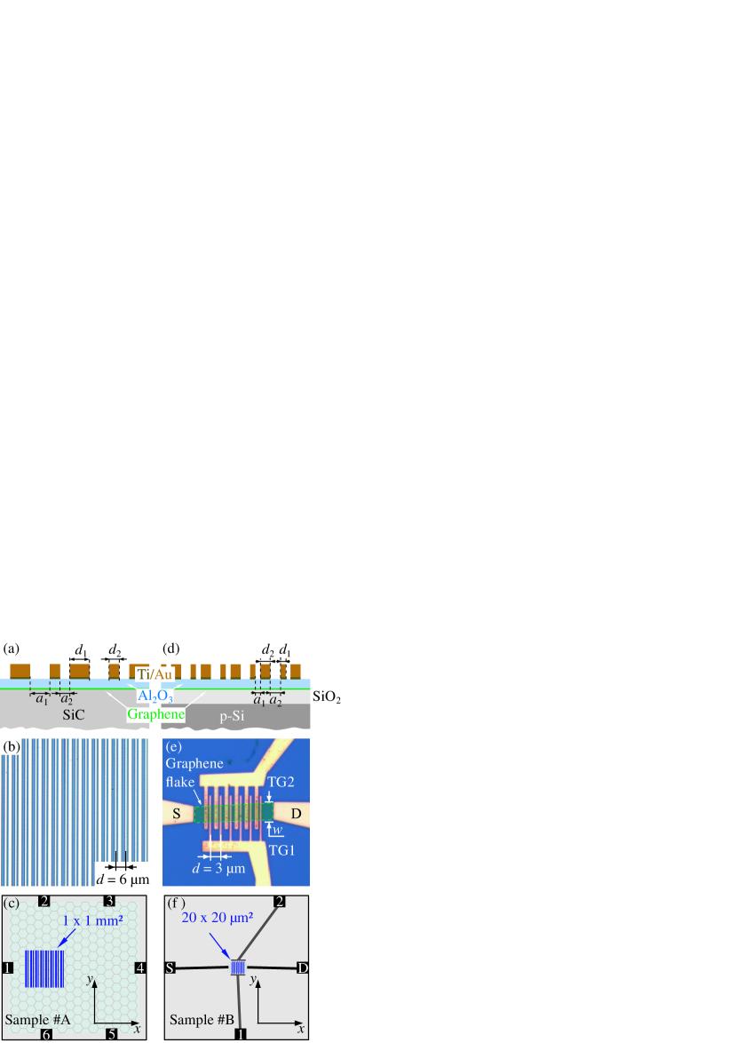
The experiments were performed using a methanol laser 3aa ; DMS2 emitting at the frequency THz (wavelength of = 118 m and photon energy = 10.5 meV). The radiation power, , being of the order of 50 mW at the sample surface, has been controlled by pyroelectric detectors and focused onto samples by a parabolic mirror. The beam shape of the THz radiation is almost Gaussian, checked with a pyroelectric camera Ganichev1999 ; Ziemann2000 . The peak intensity in the laser spot on the sample, being of about 1.5 mm diameter footnote , was W/cm2. The THz radiation polarization state was varied by rotation of crystal quartz /4- and /2-plates book . To obtain circular and elliptically polarized radiation, the quarter-wave plate was rotated by an angle between the initial polarization plane and the optical axis of the plate. The radiation polarization states for several angles are illustrated on top of Fig. 3. The orientation of the linearly polarized radiation is defined by the azimuthal angle with chosen in such a way that the electric field of the incident linearly polarized radiation is directed along the -direction, i.e. perpendicular to the metal fingers. The ratchet photocurrents have been measured in graphene structures at room temperature as a voltage drop across a 50 or 470 load resistance, . The photovoltage signal is detected by using standard lock-in technique. The photocurrent relates to the photovoltage as because in all experiments described below the load resistance was much smaller that the sample resistance (). The corresponding photocurrent density is obtained as , where is the width of the two-dimensional grating-gate structure being 1 mm for samples type #A and 5 m for samples type #B.
III Experimental results
III.1 Photocurrents in large area epitaxial graphene structures
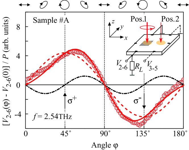
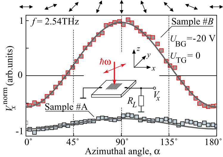
First we discuss the results obtained from the large scale lattice prepared on the top of epitaxial graphene layer. Irradiating the structure with the THz beam, position 1 in Fig. 3, we detected a polarization dependent photocurrent. Figure 3 shows the corresponding photovoltage, , measured in the direction along the metal fingers (-direction) as a function of the angle governing the radiation ellipticity. The signal varies with the radiation polarization as , where is a polarization independent offset which is obtained as at footnote3 . The figure reveals that the signal is dominated by the circular photocurrent being proportional to the degree of circular polarization and reversing its direction by inverting of the THz radiation helicity. The second contribution to the signal, , whose amplitude is about three times smaller than , corresponds to the photocurrent driven by the linearly polarized radiation and vanishes for circularly polarized radiation. In experiments applying half-wave plates it varies with the azimuth angle as (not shown). Note that the functions and describe the degree of linear polarization of THz electric field in the coordinate frame rotated by in respect to the axes Review_JETP_Lett . Our experiments were performed on several identically patterned samples. Though they were processed and structured identically, we observe different ratios of the linear and circular component for the same wavelength. As we show below, this fact can be attributed to slightly different intrinsic transport relaxation times (charge carrier mobilities) in the samples.
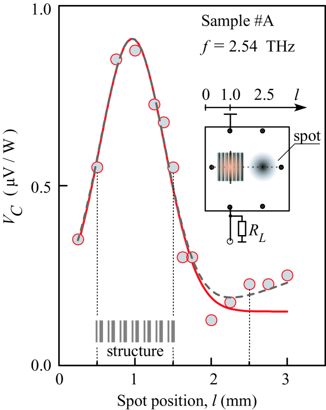
Shifting the beam spot away from the structured area, position 2 in Fig. 3, and measuring the signal either from contacts 2-6 or 3-5 we observe the signal reduced by an order of magnitude. This observation indicates that the photocurrent stems from the irradiation of the superlattice. To provide additional evidence for this conclusion we scanned the laser spot across the sample along the -direction. The photocurrent was measured between contacts 2 and 6 aligned along the metal stripes, i.e. along the -direction. The experimental geometry and the circular photocurrent as a function of the radiation spot position are shown in Fig. 4. The current reaches its maximum for the laser spot centered at the superlattice and rapidly decays with the spot moving away. Comparison of with the curve calculated assuming that the signal stems from the lateral structure only and by using the laser beam spatial distribution measured by a pyroelectric camera shows that the signal follows this curve. This observation unambiguously demonstrates that the photocurrent is caused by irradiating the superlattice. It also excludes photocurrents emerging due to possible radiation-induced local heating causing the Seebeck effect, as such a signal should obviously reverse its sign at the middle of the sample. The only deviation from this behaviour is detected for large values of at which the signal starts growing again. This result is attributed to the generation of the edge photocurrents reported in Refs. Glazov2014 ; Karch_PRL_2011 . For large -values the beam spot reaches the edge of the graphene sample resulting in a photocurrent caused by the asymmetric scattering at the graphene edge Karch_PRL_2011 . The ratchet photosignal is also observed in the direction perpendicular to the fingers, i.e. along the -direction. In this case the signal is insensitive to the THz electric field handedness and varies only with the degree of linear polarization as or , see Figure 5 showing as a function of the azimuthal angle . The same dependence has been measured in the DGG device, sample #B in Fig. 5, indicating that the DGG structure features the same superlattice effect as the large-area one (sample #A). As we show below, the appearance of the photocurrent along and accross the periodic structure as well as its polarization dependence are in full agreement with the ratchet effects excited by polarized THz electric field in asymmetric lateral superlattices. The overall qualitative behaviour of the photocurrent is also in agreement with that of the electronic ratchet effects observed in semiconductor quantum well structures with a lateral superlattice Olbrich_PRL_09 ; Olbrich_PRB_11 ; Review_JETP_Lett . So far the properties of graphene were not manifested explicitly. The Dirac fermion properties of charge carriers in graphene manifest themselves in superlattices of type #B with independently controlled gates.
III.2 Photocurrents in inter-digitated dual-grating gates graphene structures
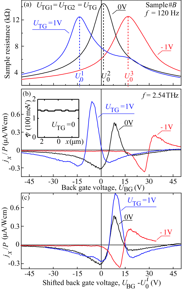
The ratchet effects are expected to be strongly dependent on the in-plane asymmetry of the electrostatic potential and near field effects of the radiation diffraction Review_JETP_Lett ; Theory_PRB_11 ; popov2013 ; Popov2015 . To demonstrate the effect of the asymmetry and examine the ratchet effects in the vicinity of Dirac point we studied samples with an inter-digitated dual-grating structure, see Figs. 1(d)-(f). In the DGG structures the degree of asymmetry can be controllably varied by applying different potentials to the top grating gates. Moreover, using the back gate voltage , we can globally change the background carrier density in the graphene flake. When the top gates are both grounded, the resistance exhibits one maximum upon tuning the back gate voltage. The maximum corresponds to the Dirac point and is detected close to zero voltage, which confirms low residual doping of graphene, Fig. 6(a). When we apply a voltage to the top gates, the back gate voltage corresponding to the Dirac point is shifted due to stray coupling of the top grating gates into the entire graphene. Furthermore, the top gates strongly modulate the carrier density in graphene directly underneath them, leading to an additional weak resistance maximum in the back gate response. Applying voltages of different polarity to different top grating gates results in a superpostition of resistance maxima corresponding to the Dirac points underneath and between the gate fingers (not shown here). We observe a slight hysteresis in the back gate sweep (shift of the resistance maximum position by V), which is probably due to the measurement being performed in the ambient air. When we set the TG1 voltage to V and TG2 voltage to V, we observe a splitting of the Dirac peak into three peaks (not shown), corresponding to regions with three different carrier densities: underneath the top gates TG1 and TG2 and in between the gate stripes, respectively.
Due to technological reasons (presence of the subgrating gates) the photocurrent in DGG structures can be examined only in source-drain direction, i.e. normal to the gate stripes footnote2 . In the following experiments aimed to study the photocurrent as a function of the back gate voltage for differently biased top gates we used the THz radiation polarized along the source-drain direction. Figure 6(b) shows obtained for the three equal values of top gate voltages, . The photocurrent shows a complex sign-alternating behaviour with enhanced magnitude in the vicinity of the Dirac points being characterized by resistance maxima and sign inversion for and V. The photocurrents have opposite directions at very high (above V) and at high negative back gate voltages. Figure 6(b) demonstrates that while the overall dependencies of the photovoltage obtained at different top gate potentials are very similar they are shifted with respect to each other to that in the transport curves. This is clearly seen in Fig. 6(c) where the curves for non-zero top gate voltages are shifted by the back gate voltage at which the resistance achieves maximum at corresponding , see Fig. 6(a). The figure reveals that the current can change its sign in the vicinity of the Dirac point. This fact can naturally be attributed to the change of carrier type from positively charged holes to negatively charged electrons footnote4 .
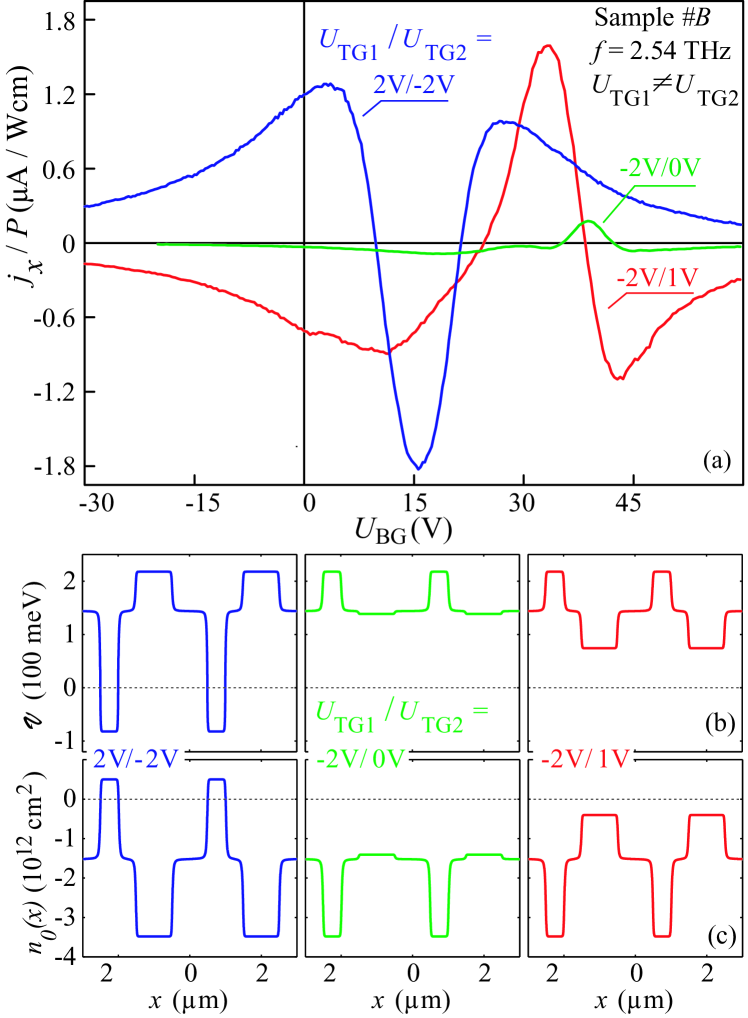
In order to tune the lateral asymmetry, we applied different bias voltages to the grating subgates. Figure 7 shows the photocurrent obtained for (i) V, V, (ii) V, V, and (iii) V, . For cases (i) and (ii), the potential asymmetry is efficiently inverted and hence we obtain inverted photocurrents far away from the Dirac point, i.e. at large values of . These observations show that the photocurrent is caused by the excitation of the free carriers in graphene beneath the superlattice and its direction depends on the sign of the in-plane asymmetry of the electrostatic potential. More complicated behaviour is detected in the vicinity of the Dirac points. Here, the polarity of the free-carrier distribution in graphene and hence that of the photocurrent strongly depend on the voltage set at the top gates. This causes a more complicated variation of the photocurrent (including its sign reversal) as a function of the back gate voltage, , around the Dirac point. Comparing the magnitudes of the signals for equal and unequal top gate voltages [Fig. 6(b) and Fig. 7(a), respectively] we see that in the latter case the photocurrent is several times enhanced. Finally, we note that if only one of top gates is biased, the signal vanishes for almost all back gate voltages. The calculation of the electrostatic potential indeed reveals that the potential becomes almost symmetric in this case indeed.
To summarize, experiments on two different types of graphene structures provide a self-consistent picture demonstrating that the photocurrents (i) are generated due to the presence of asymmetric superlattices, (ii) are characterized by specific polarization dependencies for directions along and across the metal stripes, (iii) changes the direction upon reversing the in-plane asymmetry of the electrostatic potential as well as changing the carrier type, (iv) are characterized by a complex sign-alternating back gate voltage dependence in the vicinity of the Dirac point, and (v) are strongly enhanced around the Dirac point.
IV Discussion
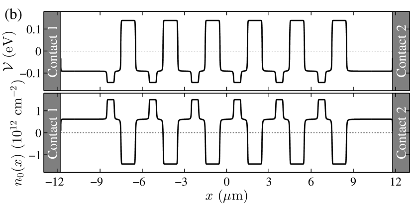
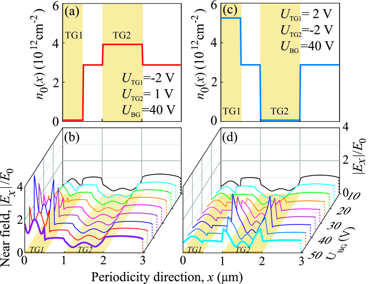
Now we discuss the origin of the ratchet current in graphene with an asymmetrical grating irradiated by the THz beam. The effect of the grating is twofold: (i) it generates a one-dimensional periodic electrostatic potential acting upon the 2D carriers and (ii) it causes a spatial modulation of the THz electric field due to the near field diffraction book . Figures 8(a) and 8(b) show calculated coordinate dependencies of the free carrier density and THz electric near-field for the DGG structure #B for two combinations of the top and back gate voltages. The electric field distribution caused by the near field diffraction is calculated for radiation with the frequency THz applying a self-consistent electromagnetic approach based on the integral equation method described in detail in Ref. Fateev2010 , see also Appendix A. Figures 8 demonstrates that both the carrier density and THz field acting on charge carriers in the -direction are asymmetric and their distribution is strongly affected by the voltages applied to the individual top gratings. These one-dimensional asymmetries result in the generation of a electric current. As we show below the ratchet current may flow perpendicular to the metal fingers or along them. The mechanism leading to the photocurrent formation can be illustrated on the basis of the photocurrent caused by the Seebeck ratchet effect (thermoratchet). This type of the ratchet currents can be generated in the direction perpendicular to the metal stripes and corresponds to the photocurrent in Fig. 5. The spatially-modulated electric field of the radiation heats the electron gas changing the effective electron temperature from the equilibrium value to footnoteLG . Here is the average electron temperature and oscillates along the -direction with the superlattice period . In turn, the nonequilibrium correction causes an inhomogeneous correction to the dc conductivity, . Taking into account the space modulated electric field we obtain from Ohm’s law the thermoratchet current in the form Theory_PRB_11
| (1) |
Here is the electron charge, and angular brackets denote averaging over a spacial period. This photocurrent vanishes if the temperature is not space-modulated, therefore it is called the Seebeck ratchet current footnoteT1 .
Besides the thermoratchet effect the THz radiation can induce additional photocurrents being sensitive to the linear polarization plane orientation or to the helicity of circularly polarized photoexcitation. In the classical regime achievable in our experiments and characterized by where is the Fermi energy, all these photocurrents can be well described by means of Boltzmann’s kinetic equation for the coordinate dependent distribution function . It has the following form:
| (2) |
where is the velocity of an electron with the wavevector being equal in graphene to , m/s is the Dirac fermion velocity, is the collision integral, and is the periodic force acting on charged carriers
| (3) |
where is the unit vector in the -direction. In terms of the distribution function the electric current density is written as
| (4) |
where the factor 4 accounts for the spin and valley degeneracies in graphene. In the next section we present the theory of the ratchet currents which is valid for arbitrary large and abrupt periodic electrostatic potentials , and results of numerical calculations based on the developed theory and the complex distribution of the near field. However, in order not to overload the discussion of the experimental results with cumbersome equations, we first follow Refs. Olbrich_PRL_09 ; Olbrich_PRB_11 ; Review_JETP_Lett ; Theory_PRB_11 and present solutions of the Boltzmann equation for weak and smooth electrostatic potential and the electric near-field. Iterating the Boltzmann Eq. (2) for small , and their gradients, and ignoring the birefringence effect under the grating gate IvchenkoPetrovFTT2014 ; footnoteStokes , we obtain the dc current density components and :
| (5) | |||
| (6) |
For incident radiation, the combinations bilinear in the field amplitudes vary upon rotation of quarter- and half-wave plates as footnoteStokes
| (7) | |||
| (8) | |||
| (9) |
All photocurrent contributions are detected in experiment, see Figs. 3 and 5. The coefficient corresponds to the thermoratchet current discussed above. This photocurrent can be generated in the in-plane direction normal to the metal stripes. In experiments it yields the signal , see Fig. 5. The part of the signal detected for the same direction and varying upon rotation of the linear polarization, in Fig. 5, is given by the second term in the right hand side of Eq. (5) and is proportional to footnoteSeebeck . The linear () and circular photocurrents observed in the direction along the metal stripes correspond to the first and second terms in the right hand side of Eq. (6) and describe the linear () and circular () ratchet effects, respectively. The polarization dependent contributions appear because the free carriers in the laterally modulated graphene can move in the two directions () and are subjected to the action of the two-component electric field with the and components.
Now we discuss the role of the superlattice asymmetry in the thermoratchet current formation. Taking the lateral-potential modulation and the electric-field in the simplest form:
| (10) |
| (11) |
with , we obtain for the average Theory_PRB_11
| (12) |
The above phenomenological equations reveal that the thermoratchet current can be generated only if the lateral superlattice is asymmetric. The asymmetry, created in our structures due to different widths of the metal fingers and spacings between them (Fig. 1), causes a phase shift between the spatial modulation of the electrostatic lateral potential gradient and the near-field intensity yielding a non-zero space average of their product. The role of the superlattice lateral asymmetry and peculiarities of the graphene band structure are explored in the experiments on the inter-digitated DGG structures. The back gate and the two independent top subgrating gates enabled us to controllably change the free carrier density profile in the -direction. Let us begin with the data for equal top gate potentials shown in Fig. 6. At zero top gate voltages the asymmetry is created by the build-in potential caused by the metal stripes deposited on top of graphene. Transport data reveal that at zero back gate voltage we deal with graphene almost at the charge neutrality point. The photocurrent shows a complex behaviour upon variation of the back gate voltage. First of all it has the opposite polarities at large positive and negative back gate voltages. This fact can be primarily attributed to the change of the carrier type in graphene which results in the reversal of the current direction. At moderate back gate voltages the amplitude of the photocurrent substantially increases whereas in the vicinity of the Dirac point it exhibits a double sign inversion. The origin of this behaviour is unclear. First of all, it may be caused by possible band-to-band optical transitions which become allowed at Dirac point because the double Fermi energy can be smaller than the photon energy in this case. Also, as mentioned in the previous section, the sign of the free-carrier distribution in graphene and hence that of the photocurrent strongly depend on the voltage set at the top gates which causes a more complex variation of the photocurrent (including a photocurrent sign reversal) as a function of the back gate voltage around the Dirac point.
Figure 6 demonstrates that the application of a positive or negative voltage to both top gates does not change qualitatively the photocurrent behaviour but shifts the dependence as a whole to smaller or larger back gate voltages in full correlation with the shift of the charge neutrality point documented by transport measurements. These results show that the current is proportional to the charge sign of the carriers (negative for electrons, positive for holes) in graphene. Figure 6(c) reveals that the photocurrent reverses its direction under inversion of the top gate voltage from +1 V to V. This fact is also in agreement with Eq. (5). Indeed, at small amplitude of the potential, the photocurrent is . This average changes sign upon the inversion of the potential . Even a more spectacular role of the in-plane asymmetry is exhibited in the experiments on the DGG structure with different polarities of the gate voltages applied to TG1 and TG2. First of all, the difference in the potentials increases the asymmetry resulting in the photovoltage enhancement by more than an order of magnitude for large positive and negative gate voltages, Figs. 6 and 7. Moreover, the change of the relative polarity of the TG1 and TG2 gate voltages results in a reversed photocurrent direction for all back gate voltages clearly reflecting the sign inversion of the static potential asymmetry given by . Figure 7 also shows that for a certain combination of the top gate voltages ( V and ) the photocurrent almost vanishes. This fact will be discussed in the next section presenting calculations of the photocurrent for exact profiles of the electrostatic potential and radiation near field.
Summarizing the discussion, all experimental findings can consistently be explained qualitatively by the free carrier ratchet effects. A quantitative analysis is presented in the Sec. V.
V Theory
V.1 Photocurrent in the direction normal to the grating stripes
Three microscopic mechanisms of the ratchet current are considered and compared: (i) the Seebeck contribution generated in the course of the photoinduced spatially modulated heating of the free carriers accompanied by a periodic modulation of the equilibrium carrier density; (ii) the polarization-sensitive current controlled by the elastic scattering processes and (iii) differential plasmonic drag. The main difference the first two mechanisms as compared with those in lateral quantum-well structures Review_JETP_Lett is determined by specific properties of graphene, namely, (i) the linear, Dirac-like, dispersion of free-carrier energy, and (ii) the degenerate statistics of the free-carrier gas in doped (or gated) graphene even at room temperature.
The photocurrent flowing in the periodicity direction is given by
| (13) |
Here the first term is the Seebeck ratchet current. The second term is caused by pure elastic scattering processes which are not related to carrier heating Theory_PRB_11 , it yields a polarization dependent photocurrent varying upon rotation of the radiation polarization plane. The photocurrent is caused by the differential plasmonic drag popov2013 ; Popov2015 .
We apply the kinetic theory for calculating the Seebeck ratchet current. For degenerate statistics it yields (see Appendix B):
| (14) |
Here and are the free carrier momentum and energy relaxation times, respectively. The derived expression for the Seebeck ratchet current is valid for arbitrarily large and abrupt periodic potential . We assume the Fermi energy to lie high above the Dirac point and take into account only one sort of free carriers, namely, the electrons. The similar results are obtained for the Fermi energy lying deep enough in the valence band in which case the electron representation is replaced by the hole representation. Due to the charge-conjugation symmetry between electrons and holes in graphene, the current (14) reverses under the changes , and , where the energy is referred to the Dirac point. We also note that this current vanishes if the -coordinate dependence of the near field intensity is a composite function . One more symmetry property follows for a low-amplitude potential : in this case the current reversal occurs just at the potential inversion .
The differential plasmonic drag photocurrent induced in the grating-gated graphene by the normally incident THz radiation can be estimated as, see Appendix C,
| (15) |
where are the Fourier-space harmonics of the in-plane component of the near-electric field in graphene with where is an integer. It is worth noting that the differential plasmonic drag Popov2015 can be also viewed phenomenologically as a specific ”linear” ratchet effect induced in a periodic graphene structure by the normally incident THz radiation with the electric field polarized perpendicular to the grating gate.
We simulate the interaction of THz radiation incident normally upon the grating-gated graphene in the framework of a self-consistent electromagnetic approach based on the integral equation method described in detail in Ref. Fateev2010 . The calculations are performed for the characteristic parameters of the DGG structure used in the experiment (see Appendix A). In our simulations, we assume the metal grating stripes to be perfectly conductive and infinitely thin. This is a quite justified and commonly used assumption at THz (and lower) frequencies where metals are characterized by a high real conductivity. As a result of the electromagnetic modeling, we obtain the in-plane component of the near-electric field in graphene entering Eqs. (14), (15). Periodic electrostatic potential in graphene is created by applying different electric voltages to the two different subgratings of the DGG. It should be noted that the periodic electrostatic potential is induced in graphene even for zero voltage at each subgrating due to finite density of states in graphene (the quantum capacitance effect). The profiles of the calculated near-electric field and the free-carrier density are shown in Figs. 8 (b) and (d) for various voltages applied to different subgratings of the dual-grating gate at frequency 2.54 THz. It is seen that the near-electric field is asymmetric relative to equilibrium free-carrier density profile in graphene. This gives rise to the Seebeck (thermoratchet) photocurrent Eq. (14).
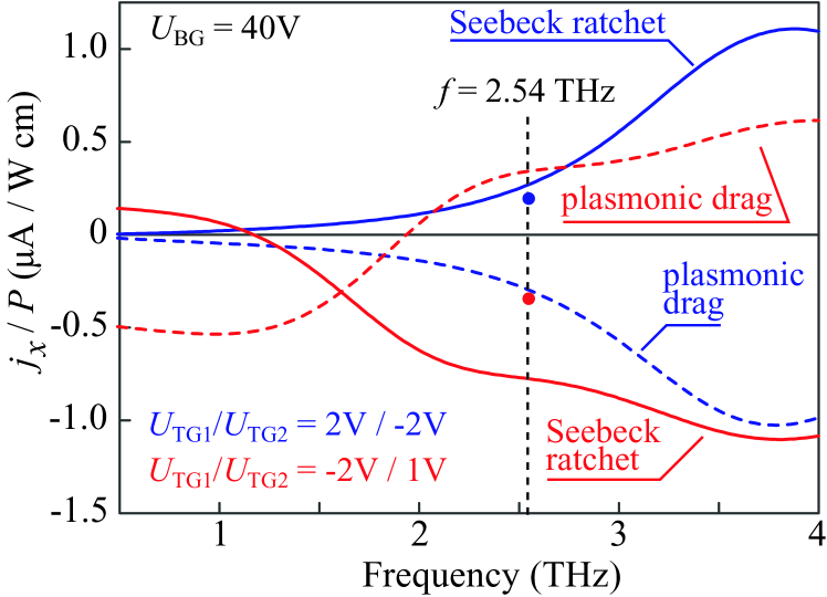
The calculated thermoratchet photocurrent as a function of frequency is shown by solid curves in Fig. 9 for various voltages applied to different subgratings of the DGG for monopolar graphene charged by applying large positive voltage to the back gate electrode. In this situation we deal with electrons in graphene under the metal fingers and between them even for negative voltages applied to a top gate. It is worth noting that the magnitude of the photocurrents as well as the inversion of the photocurrent direction for reversing of relative signs of voltages applied at different subgratings of the top dual-grating gate are in a accordance with the experimental observations at the frequency 2.54 THz (Fig. 9).
The calculated differential plasmonic drag photocurrent (15) as a function of frequency is shown by dashed curves in Fig. 9. It follows from the figure that, as well as for the thermoratchet photocurrent, the inversion of the voltage signs at different subgratings of the top dual-grating gate changes the sign of the plasmonic-drag photocurrent. However, the plasmonic-drag photocurrent is directed oppositely to the thermoratchet photocurrent. Therefore, the plasmonic-drag photocurrent can compensate or, for a certain combination of top gate voltages, even cancel the thermoratchet photocurrent diminishing the total photocurrent generated in graphene by the incident THz radiation. This fact may be responsible for the vanishingly small photocurrent observed for V and , Fig. 7.
V.2 Photocurrent in the direction along the grating stripes
Solution of the Boltzmann equation (2) also yields the component of the photocurrent. In order to derive the expression for for the electrostatic potential comparable to the Fermi energy, we assume that both energy relaxation and diffusion are less effective than elastic scattering: , but the product can be arbitrary. Here is the diffusion constant of the Dirac fermions in graphene. We consider the elastic scattering by a long-range Coulomb potential. In this case, the momentum relaxation time in non-structured graphene is a linear function of the Fermi energy: . Therefore, in the structures with a lateral superlattice under study we have . Using the procedure described in Ref. Theory_PRB_11 , we obtain the photocurrent component along the grating stripes in the form of Eq. (6):
| (16) |
where the coordinate dependence of the coefficients and is given by
| (17) | ||||
The coefficients and describe the linear and circular ratchet effects, respectively. The linear polarization-dependent and helicity-dependent combinations of the products and which determine the photocurrent are related to the corresponding combinations of the incident radiation as follows IvchenkoPetrovFTT2014 :
A presence of imaginary part is caused by effective birefringence of the studied low-symmetry structure resulting in an ellipticity of the near-field polarization under incidence of pure circularly or pure linearly (in the frame ) polarized radiation.
VI Conclusion
To summarize, we have demonstrated that ratchet effects driven by THz electric fields can be efficiently generated in graphene with a lateral superlattice. The ratchet photocurrent includes the Seebeck thermoratchet effect as well as the effects of “linear” and “circular” ratchets, sensitive to the corresponding polarization of the driving electromagnetic force. Studying the ratchet effect in the inter-digitated comb-like dual-grating-gate structures we have demonstrated that its amplitude and sign can be efficiently controlled by applying unequal voltages to the DGG sublattices or the back gate voltage. We have calculated the electronic and plasmonic ratchet photocurrents at large negative and positive back gate voltages taking into account the calculated potential profile and the near field acting on carriers in graphene. The understanding of the observed complex back gate dependence and strong enhancement of the ratchet effect in the vicinity of the Dirac point, however, requires further study. In particular, a theory describing ratchet effects for systems with periodic change of the carrier type is to be developed. Further development of the theory is also required for a quantitative analysis of the plasmonic ratchet effects in graphene.
Appendix A Electrostatic potential profile and near-field calculations
The one-dimensional electric potential energy profile (or more precisely local energy band offset profile) is calculated via
| (18) |
where is the equilibrium carrier density profile (positive carrier density corresponds to electrons and negative carrier density corresponds to holes in graphene) obtained by a 2D finite-element-based electrostatic simulation using FEniCS FEniCS and Gmsh gmsh , combined with the quantum capacitance model Fang2007 ; Liu2013 .
The finite-element simulation follows the device geometry of the experiment, see Figs. 1 and 2, and provides the classical self-partial capacitance for individual top gate set 1, , and set 2, , while the quantum capacitance model takes care of the correction to the net charge density due to the finite density of states of the conducting layer (here graphene) Luryi1988 . Together with the global back gate capacitance that can be described by the parallel-plate formula, the total classical carrier density is given by
| (19) |
where the summation runs over , and a uniform intrinsic doping concentration is considered in our slightly p-doped graphene sample. The net carrier density after taking into account the quantum capacitance correction reads Liu2013
| (20) | ||||
with given in Eq. (19) and . Therefore Eq. (20)gives the total carrier density as a function of position, subject to arbitrary voltage inputs, and can be inserted in Eq. (18) to finally obtain the electric potential energy profile .
The near electric field in graphene induced by a normally incident THz wave was calculated by using the self-consistent electromagnetic approach described in Ref. Fateev2010 . Calculations were performed for the characteristic parameters of the DGG structure used in the experiment: , , , , and . Dielectric constants of the graphene substrate () and the barrier layer () between graphene and the top DGG gate are 3.9 and 9 (see epsilon ), respectively. The barrier layer thickness is 30 nm. The frequency-dependent response of graphene is described by a local dynamic conductivity Falkovsky2007
| (21) |
where
| (22) |
, and the temperature is set to 300 K. The first term in Eq. (A) describes a Drude-like response involving the intraband processes with the phenomenological carrier scattering time , which can be estimated from the measured carrier mobility as Tan2007 . The second and third terms in Eq. (A) describe the interband carrier transitions in graphene.
Appendix B Derivation of the Seebeck ratchet current density
For the structures under consideration one needs to extend the theory of the Seebeck ratchet current derived in Ref. Theory_PRB_11 for a weak electron periodic potential to an arbitrarily large potential. For simplicity, we assume the Fermi energy to lie high enough above the Dirac point and consider one sort of free carriers.
The absorption of THz radiation results in an inhomogeneous heating of 2D carriers in graphene with a lateral superlattice. Similarly to Ref. Theory_PRB_11 , we present the time-independent electron distribution function as a sum of the components even and odd in , respectively, decompose the Boltzmann kinetic equation into even and odd parts, select the odd-in- part and arrive at the following equation for the function contributing to the Seebeck ratchet effect
| (23) |
Here the potential is a sum of the equilibrium potential and a correction that appears due to the radiation-induced carrier redistribution. This correction is proportional to the radiation intensity and related by the Poisson equation to a radiation-induced change where is the equilibrium electron density and
| (24) |
is the steady-state nonequilibium density. The Poisson equation is easier to express in terms of the Fourier transforms as follows
| (25) |
where æ is the dielectric constant. Hereafter the average value of the electron density is fixed which imposes the following restriction on the electron density
| (26) |
Multiplying the equation (23) by and summing over the electron spin , the valley index and the quasi-momentum we get the Seebeck ratchet current density:
| (27) |
where is the electron energy dispersion linear in graphene. The current is zero in the absence of radiation because, in equilibrium, where is the Fermi-Dirac distribution function, and hence
The current density (27) can be expressed via the conductivity
| (28) |
and the diffusion coefficient as follows
| (29) |
This result is valid in all orders in .
In what follows we assume to be independent of the particle energy . Then in graphene the coefficient equals to and is independent of . As a result, one has
| (30) |
Obviously, one can equivalently substitute the corrections and into Eq. (29) instead of and .
Before the search for and we exclude the potential from the consideration. For this purpose we decompose the electron density and the conductivity in the following form
| (31) |
Here is a local change of the electron conductivity caused by heating by the THz radiation, see below, and the functions and are auxiliary: they are found from Eqs. (24) and (28) with the exact function replaced by the auxiliary (quasi-equilibrium) function
| (32) |
where is the equilibrium Fermi energy and the correction restores the average electron density. One can check that and satisfy the equation
| (33) |
Neglecting a second-order correction proportional to we obtain an equation for the electric current determined exclusively by and the corrections , :
| (34) |
The two corrections are related with each other by
| (35) |
Here we take into account that the correction is caused by redistribution of carriers but not by heating. In contrast, the correction is due to heating at a fixed carrier density:
| (36) |
where is the average electron energy in equilibrium and is a local change of the electron average energy caused by the THz radiation. As above, the index “0” denotes functions calculated in the absence of radiation and dependent on the coordinate due to the -dependence of the static potential . The change is found from the energy balance equation
| (37) |
where is the energy relaxation time. Thus, Eq. (34) reduces to the equation
| (38) |
containing one unknown function, .
Under the requirement of coordinate independence of , Eq. (38) forms a first-order differential equation for the correction . Its solution is given by
| (39) | ||||
where
| (40) |
and a value of is determined from the condition (26). Moreover, after averaging over the space period in Eq. (38) the third contribution vanishes and we obtain
| (41) |
where the angular brackets mean averaging over . According to Eq. (39) the correction depends linearly on . Therefore, Eq. (41) is just a linear algebraic equation for the Seebeck ratchet photocurrent. Substituting from Eq. (39) and noticing that the term with does not contribute to the current [because the function depends on the coordinate via the static potential ] we finally obtain
| (42) | |||
where
| (43) |
Now we calculate the variational derivatives and . The even part of the distribution function modified by the temperature change is given by
| (44) |
where is a radiation-induced change of the local electron temperature and, in contrast to Eq. (32), the correction is varying in space due to the electron redistribution following the inhomogeneous heating. The functions , and are expressed via and
| (45) | |||
| (46) | |||
| (47) |
from whence we obtain
| (48) |
In equilibrium, the concentration, average particle energy and conductivity are obtained from the corresponding values in unstructured graphene, , and , by the substitution
| (49) |
These values depend on the Fermi energy and temperature as follows (, spin and valley degeneracies are taken into account):
| (50) |
| (51) |
| (52) |
Here are the polylogarithm functions of orders 2 and 3, respectively. At these expressions reduce with accuracy up to :
| (53) | ||||
| (54) |
This allows us to calculate the functions and :
| (55) |
Then we obtain:
| (56) |
| (57) |
and proceed from Eq. (42) for the ratchet current to
| (58) |
For ratchets based on quantum-well structures with a parabolic energy dispersion , the analogous procedure yields the Seebeck ratchet current density in the form:
| (61) | ||||
In this case, is given by
| (62) |
Appendix C Differential plasmonic drag in graphene
Let us consider a homogeneous graphene screened by an inter-digitated metal DGG. We simulate the plasmonic response of graphene by solving the hydrodynamic equations
| (63) |
| (64) |
describing the free-carrier motion in graphene, where is the electric (in general, nonlinear) current in graphene, and are the charge density and hydrodynamic velocity of the carriers in graphene, respectively, is the Fermi energy in graphene related to the carrier density as Rudin2011 , is the in-plane electric near field. Equations (63) and (64) are taken from Ref. Rudin2011 by approximating the carrier momentum for small carrier velocities, , by
Strictly speaking, the latter equation is valid for zero temperature. However, as mentioned in Section V.1, the free-carrier gas in doped (or gated) graphene is degenerate even at room temperature so that this expression is relevant also for room temperature. We also neglect the terms describing the carrier pressure and viscosity contributions in Eq. (64) which are responsible for the non-locality effects in the plasmonic response.
Nonlinearity of the free carrier motion in graphene described by Eqs. (63) and (64) originates from (i) the product defining the conductive current , (ii) the second term in Eq. (64) describing the nonlinear convection current, and (iii) the dependence of the oscillating Fermi energy on the applied electric-field amplitude . It is worth noting that all the three sources of the nonlinearity survive only if an inhomogeneous (i.e., the -dependent) carrier-density oscillations occur in graphene. Therefore, these nonlinearities essentially are of the plasmonic nature.
We solved the hydrodynamic equations (63) and (64) in the perturbation approach Aizin2007 by expanding every unknown variable in powers of the electric field amplitude and keeping only linear and quadratic terms in this expansion. Then the induced current density in graphene is given by , where is the equilibrium carrier density, and and are the linear corrections to the density and velocity of free carriers in graphene, respectively.
Time averaging of yields the rectified current
| (65) |
where are the amplitudes of the spatial Fourier harmonics of the plasmonic electric field , and is an integer. It follows from Eq. (65) that the dc photocurrent appears only for , due to the differential drag of the carriers by the counter-directed Fourier harmonics of the plasmonic near field. The differential plasmonic photocurrent has the opposite polarities depending on the electron or hole conductivity of graphene. In distinction from conventional 2D electron system Popov2015 , the prefactor in the sum (65) is independent of the equilibrium carrier density which means that Eq. (65) for the differential plasmonic drag current is valid for both a homogeneous and periodically modulated graphene. However, additional contributions to the plasmonic ratchet photocurrent, which can appear in graphene with spatially modulated carrier density, requires further analysis.
Acknowledgments
Financial support via the Priority Program 1459 Graphene of the German Science Foundation DFG and the Russian Foundation for Basic Research are gratefully acknowledged.
References
- (1) A. H. Castro Neto, F. Guinea, N. M. R. Peres, K. S. Novoselov, and A. K. Geim, Rev. Mod. Phys. 81, 109 (2009).
- (2) F. Bonaccorso, Z. Sun, T. Hasan, and A. C. Ferrari, Nat. Photon. 4, 611 (2010).
- (3) P. Avouris, Nano Lett. 10, 4285 (2010).
- (4) S. Das Sarma, Rev. Mod. Phys. 83, 407 (2011).
- (5) A. F. Young and P. Kim, Ann. Rev. Cond. Mat. Phys. 2, 101 (2011).
- (6) J. Yan, M.-H. Kim, J. A. Elle, A. B. Sushkov, G. S. Jenkins, H. M. Milchberg, M. S. Fuhrer, and H. D. Drew, Nature Nanotech. 7, 472 (2012).
- (7) V. Ryzhii, T. Otsuji, M. Ryzhii, N. Ryabova, S. O. Yurchenko, V. Mitin, and M. S. Shur, J. Phys. D: Appl. Phys. 46, 065102 (2013).
- (8) F. H. L. Koppens, T. Mueller, Ph. Avouris, A. C. Ferrari, M. S. Vitiello, and M. Polini, Nature Nanotech. 9, 780-793 (2014).
- (9) X. Xu, N. M. Gabor, J. S. Alden, A. M. van der Zande, and P. L. McEuen, Nano Lett. 10, 562 (2010).
- (10) T. Mueller, F. Xia, and P. Avouris, Nature Photon. 4, 297 (2010).
- (11) M. Mittendorff, S. Winnerl, J. Kamann, J. Eroms, D. Weiss, H. Schneider, and M. Helm, Appl. Phys. Lett. 103, 021113 (2013).
- (12) T.J. Echtermeyer, L. Britnell, P.K. Jasnos, A. Lombardo, R.V. Gorbachev, A.N. Grigorenko, A.K. Geim, A.C. Ferrari, and K.S. Novoselov, Nature Commun. 2, 458 (2011).
- (13) L. Vicarelli, M. S. Vitiello, D. Coquillat, A. Lombardo, A. C. Ferrari, W. Knap, M. Polini, V. Pellegrini, and A. Tredicucci, Nature Materials 11, 865 (2012).
- (14) A. Tomadin and M. Polini, Phys. Rev. B 88, 205426 (2013).
- (15) A. Tredicucci and M.S. Vitiello, IEEE J. Sel. Top. Quant. Electr. 20, 8500109 (2014).
- (16) F. H. L. Koppens, T. Mueller, Ph. Avouris, A. C. Ferrari, M. S. Vitiello, and M. Polini, Nature Nanonotech. 9,780 (2014).
- (17) R. R. Hartmann, J. Kono, and M. E. Portnoi, Nanotechn. 25, 322001 (2014).
- (18) W. Knap and M. Dyakonov, in Handbook of Terahertz Technology ed. by D. Saeedkia (Woodhead Publishing, Waterloo, Canada, 2013), pp. 121-155.
- (19) W. Knap, S. Rumyantsev, M. S Pea Vitiello, D. Coquillat, S. Blin, N. Dyakonova, M. Shur, F. Teppe, A. Tredicucci, and T. Nagatsuma, Nanotechn. 24, 214002 (2013).
- (20) S. Boppel, A. Lisauskas, A. Max, V. Krozer, and H. G. Roskos, Opt. Lett. 37, 536 (2012).
- (21) M. Tonouchi, Nature Photon. 1, 97 (2007).
- (22) P. Reimann, Phys. Rep. 361, 57 (2002).
- (23) P. Olbrich, E. L. Ivchenko, R. Ravash, T. Feil, S. D. Danilov, J. Allerdings, D. Weiss, D. Schuh, W. Wegscheider, and S. D. Ganichev, Phys. Rev. Lett. 103, 090603 (2009).
- (24) P. Olbrich, J. Karch, E. L. Ivchenko, J. Kamann, B. März, M. Fehrenbacher, D. Weiss, and S. D. Ganichev, Phys. Rev. B 83, 165320 (2011).
- (25) E. L. Ivchenko and S. D. Ganichev, Pisma v ZheTF 93, 752 (2011) [JETP Lett. 93, 673 (2011)].
- (26) V.V. Popov, D.V. Fateev, T. Otsuji, Y.M. Meziani, D. Coquillat, and W. Knap, Appl. Phys. Lett. 99, 243504 (2011).
- (27) T. Watanabe, S.A. Boubanga-Tombet, Y. Tanimoto, D. Fateev, V. Popov, D. Coquillat, W. Knap, Y.M. Meziani, Yuye Wang, H. Minamide, H. Ito, and T. Otsuji, IEEE Sensors J. 3, 89 (2013).
- (28) S.A. Boubanga-Tombet, Y. Tanimoto, A. Satou, T. Suemitsu, Y. Wang, H. Minamide, H. Ito, D. V. Fateev, V.V. Popov, and T. Otsuji, Appl. Phys. Lett. 104, 262104 (2014).
- (29) Y. Kurita, G. Ducournau, D. Coquillat, A. Satou1, K. Kobayashi, S. Boubanga Tombet, Y. M. Meziani, V. V. Popov, W. Knap, T. Suemitsu, and T. Otsuji, Appl. Phys. Lett. 104, 251114 (2014).
- (30) P. Faltermeier, P. Olbrich, W. Probst, L. Schell, T. Watanabe, S. A. Boubanga-Tombet, T. Otsuji, and and S. D. Ganichev J. Appl. Phys. 118, 084301 (2015).
- (31) S. D. Ganichev, W. Weber, J. Kiermaier, S. N. Danilov, D. Schuh, W. Wegscheider, Ch. Gerl, D. Bougeard, G. Abstreiter and W. Prettl, J. Appl. Physics 103, 114504 (2008).
- (32) S.N. Danilov, B. Wittmann, P. Olbrich, W. Eder, W. Prettl, L.E. Golub, E.V.Beregulin, Z.D. Kvon, N.N. Mikhailov, S.A. Dvoretsky, V.A. Shalygin, N.Q. Vinh, A. F.G. van der Meer, B. Murdin, and S.D. Ganichev, J. Appl. Phys. 105, 013106 (2009).
- (33) A. V. Nalitov, L. E. Golub, and E. L. Ivchenko, Phys. Rev. B 86, 115301 (2012).
- (34) V. V. Popov, Appl. Phys. Lett. 102, 253504 (2013)
- (35) G. V. Budkin and L. E. Golub, Phys. Rev. B 90, 125316 (2014).
- (36) S.V. Koniakhin Eur. Phys. J. B 87, 216 (2014).
- (37) I. V. Rozhansky, V. Yu. Kachorovskii, and M. S. Shur, Phys. Rev. Lett. 114, 246601 (2015).
- (38) V. V. Popov, D. V. Fateev, E. L. Ivchenko, and S.D. Ganichev Phys. Rev. B 91, 235436 (2015).
- (39) K.V. Emtsev, A. Bostwick, K. Horn, J. Jobst, G.L. Kellogg, L. Ley, J.L. McChesney, T. Ohta, S.A. Reshanov, E. Rotenberg, A.K. Schmid, D. Waldmann, H.B. Weber, Th. Seyller, Nature Materials 8, 203 (2009).
- (40) M. Ostler, F. Speck, M. Gick, Th. Seyller, Phys. Stat. Sol. B 247, 2924 (2010).
- (41) Note that at oblique incidence we detected a photocurrent caused by the THz photon drag (dynamic Hall) effect which, however, vanishes for normal incidence Karch_PRL_2010 ; Glazov2014 .
- (42) J. Karch, P. Olbrich, M. Schmalzbauer, C. Zoth, C. Brinsteiner, M. Fehrenbacher, U. Wurstbauer, M. M. Glazov, S. A. Tarasenko, E. L. Ivchenko, D. Weiss, J. Eroms, R. Yakimova, S. Lara-Avila, S. Kubatkin, and S. D. Ganichev, Phys. Rev. Lett. 105, 227402 (2010)
- (43) M.M. Glazov and S.D. Ganichev, Physics Reports 535, 101 (2014).
- (44) M. Staab, M. Matuschek, P. Pereyra, M. Utz, D. Schuh, D. Bougeard, R.R. Gerhardts, and D. Weiss, New J. Phys. 17, 043035 (2015).
- (45) A. Logg, K.-A. Mardal, and G. N. Wells, Automated Solution of Differential Equations by the Finite Element Method (Springer, 2012).
- (46) C. Geuzaine and J.-F. Remacle, Int. J. Numerical Methods in Engineering 79, 1309 (2009).
- (47) S. Luryi, Appl. Phys. Lett. 52, 501 (1988).
- (48) T. Fang, A. Konar, H. Xing, and D. Jena, Appl. Phys. Lett. 91, 092109 (2007).
- (49) M.-H. Liu, Phys. Rev. B 87, 125427 (2013).
- (50) S.D. Ganichev, S.A. Tarasenko, V.V. Bel’kov, P. Olbrich, W. Eder, D.R. Yakovlev, V. Kolkovsky, W. Zaleszczyk, G. Karczewski, T. Wojtowicz, and D. Weiss, Phys. Rev. Lett. 102, 156602 (2009).
- (51) P. Olbrich, C. Zoth, P. Lutz, C. Drexler, V. V. Bel’kov, Ya. V. Terent’ev, S. A. Tarasenko, A. N. Semenov, S. V. Ivanov, D. R. Yakovlev, T. Wojtowicz, U. Wurstbauer, D. Schuh, and S.D. Ganichev, Phys. Rev. B 85, 085310 (2012).
- (52) S. D. Ganichev, Physica B 273-274, 737 (1999), topical review.
- (53) E. Ziemann, S.D. Ganichev, I.N. Yassievich, V.I. Perel, and W. Prettl, J. Appl. Phys. 87, 3843 (2000).
- (54) Note that the laser spot with 1.5 mm diameter is smaller than the large-area epitaxial graphene sample size allowing to avoid illumination of contacts or edges, which could result in edge currents Karch_PRL_2011 .
- (55) J. Karch, C. Drexler, P. Olbrich, M. Fehrenbacher, M. Hirmer, M. M. Glazov, S. A. Tarasenko, E. L. Ivchenko, B. Birkner, J. Eroms, D. Weiss, R. Yakimova, S. Lara-Avila, S. Kubatkin, M. Ostler, T. Seyller, and S. D. Ganichev, Phys. Rev. Lett. 107, 276601 (2011)
- (56) S. D. Ganichev and W. Prettl, (Oxford University Press, Oxford, 2006).
- (57) While being detected in all reported measurements a polarization independent offset given by the coefficient will not be discussed in details. Instead, hereafter we focus on helicity sensitive photocurrent, , and currents driven by linearly polarized light, and .
- (58) Note that to measure the circular effect we would need to detect current in the -direction. However, necessity of the gate contact does not allow to fabricate them.
- (59) Note that due to the addressed above hysteresis in the back gate sweep the exact assignment of the photocurrent nodes and maxima with respect to the Dirac point is not possible.
- (60) D.V. Fateev, V.V. Popov, and M.S. Shur, Semicond. 44, 1406 (2010).
- (61) Here we assume the Boltzmann statistics for clarity. The case of the Fermi-Dirac statistics and real situation of degenerate carriers are studied in Sec. V and Appendix B.
- (62) Hereafter we consider a graphene sheet with the lateral potential . The electron energy in each valley, or , is given by , and the two-dimensional wave vector is referred to the vortex of the hexagonal Brillouin zone. Since in the model under consideration the behavior of electrons in the or valleys is identical we consider the current generation in one of them and then double the result.
- (63) E. L. Ivchenko and M. I. Petrov, Phys. Solid State 56, 1833 (2014).
- (64) Note that the response to the polarized radiation may change due to the presence of the grating-gate polarizer as discussed in details below, see Sec. VB.
- (65) Note that while the Seebeck thermoratchet photocurrent itself does not depend on the radiation polarization. Its magnitude in response to polarized radiation may change due to the presence of the grating-gate polarization effect.
- (66) K.Z. Rajab, M. Naftaly, E.H. Linfield, J.C. Nino, D. Arenas, D. Tanner, R. Mittra, and M. Lanagan, J. Micro. and Elect. Pack. 5, 101 (2008).
- (67) L.A. Falkovsky and A.A. Varlamov, Eur. Phys. J. B 56, 281 (2007).
- (68) Tan Y-W, Zhang Y, Bolotin K, Zhao Y, Adam S, Hwang E H, Das Sarma S, Stormer H L, and Kim P, Phys. Rev. Lett. 99, 246803 (2007).
- (69) S. Rudin, Int. J. High Speed Electron. and Systems 20, 567 (2011).
- (70) G.R. Aizin, D.V. Fateev, G.M. Tsymbalov, and V.V. Popov, Appl. Phys. Lett. 91, 163507 (2007).