Sensitive radio-frequency measurements of a quantum dot by tuning to perfect impedance matching
Abstract
Electrical readout of spin qubits requires fast and sensitive measurements, which are hindered by poor impedance matching to the device. We demonstrate perfect impedance matching in a radio-frequency readout circuit, using voltage-tunable varactors to cancel out parasitic capacitances. An optimized capacitance sensitivity of is achieved at a maximum source-drain bias of V root-mean-square and with a bandwidth of 18 MHz. Quantum dot Coulomb blockade is measured in both conductance and capacitance, and the two contributions are found to be proportional as expected from a quasistatic tunneling model. We benchmark our results against the requirements for single-shot qubit readout using quantum capacitance, a goal that has so far been elusive.
I Introduction
Measuring the quantum state of an electronic device with high fidelity requires sensitive, fast, and non-invasive readout. If the state can be mapped to an electrical impedance, this can be achieved using radio-frequency reflectometry of an electrical resonator incorporating the quantum device Schoelkopf et al. (1998). This permits rapid readout of charge sensors Cassidy et al. (2007); Reilly et al. (2007), spin qubits Barthel et al. (2010), and nanomechanical resonators LaHaye et al. (2009), as well as complex impedance measurements of quantum dot circuits Petersson et al. (2010); Chorley et al. (2012); Jung et al. (2012); Schroer et al. (2012); Colless et al. (2013); Gonzalez-Zalba et al. (2015). For optimal sensitivity, which can approach the quantum limit Xue et al. (2009), impedance matching between the device and the external circuitry is essential to maximize power transfer between them Aassime et al. (2001). This is made challenging by the large resistance typical of quantum dot devices (100 k, compared with usual line impedance ), and by parasitic capacitances in the matching circuit which vary unpredictably between devices.
We present a circuit that achieves controllable perfect matching with a high device impedance, even accounting for parasitics. Voltage-tunable capacitors allow in situ tuning of the matching condition Müller et al. (2010); Hellmüller et al. (2012) and an absolute calibration of the capacitance sensitivity. We measure the complex impedance of a Coulomb-blockaded quantum dot, finding that the capacitance changes in proportion to the conductance. This relation is in agreement with a quasi-static model of electron tunneling.
II Reflectometry with perfect impedance matching
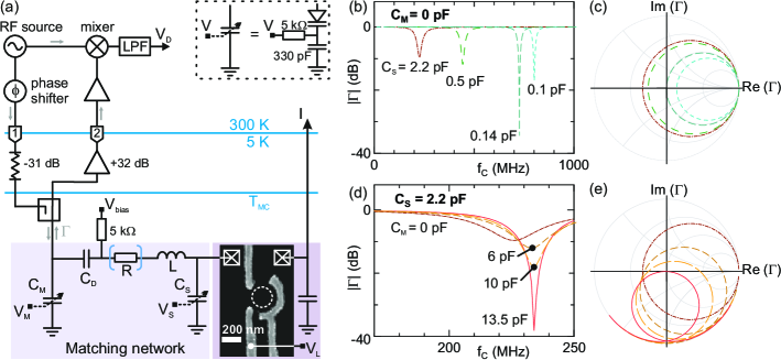
We implement the matching scheme using as the device under test a gate-defined GaAs quantum dot, measured in a dilution refrigerator as shown in Fig. 1(a). The impedance matching network is realized with a chip inductor and capacitors , forming a resonant circuit incorporating the device. To make a reflectometry measurement, a radio-frequency signal with frequency , injected at port 1 of the cryostat, is coupled via a directional coupler to the matching network input. The reflected amplified signal is returned to port 2. From the amplitude and phase of this signal, the reflection coefficient of the resonant circuit and therefore the complex impedance of the device can be deduced. A room-temperature homodyne detection circuit demodulates a chosen quadrature of the reflected signal to a DC signal . Simultaneous DC transport measurements are made using a tee to apply a bias voltage .
In previous work Schoelkopf et al. (1998); Reilly et al. (2007); Cassidy et al. (2007); Petersson et al. (2010); Chorley et al. (2012); Müller et al. (2010), the impedance match is usually hindered by parasitic capacitances. Even with careful engineering, sample wiring typically contributes a sample capacitance pF in parallel with the device Hornibrook et al. (2014). In our experiment, these parasitic capacitances are mitigated by adding a matching capacitors and a decoupling capacitor at the input of the matching network. This is illustrated in Fig. 1(b) to (e), which show simulated reflection coefficient as a function of frequency for typical device parameters. With no matching capacitor (Fig. 1(b) and (c)), perfect matching (indicated by zero reflection) is achieved only for one value of , in this case 0.14 pF. With a parasitic capacitance above this value, perfect matching cannot be achieved at any carrier frequency , degrading the sensitivity. One approach to restore matching is to increase the inductance ; however, this reduces the readout bandwidth, and more problematically introduces self-resonances of the inductor close to the operating frequency. Our approach is to introduce the capacitor to cancel out a reactive contribution to the impedance. By increasing , a perfect match can be achieved even with a much larger value of (Fig. 1(d) and (e)). In this scheme, the purpose of is to increase slightly the quality factor of the circuit by decoupling it from the input.
This scheme is implemented using varactors (Macom MA46H204-1056) for and , controlled by voltages and , so that the parameters of the matching network can be tuned in situ (Fig. 2). The device under test is a laterally defined quantum dot Mavalankar et al. (2013), fabricated by patterning Ti/Au gates over a GaAs/AlGaAs heterostructure containing a two-dimensional electron gas (depth 90 nm, mobility 125 m2V-1s-1, carrier concentration m-2). The device chip was bonded to a printed circuit board mounted with components of the matching circuit. Bias voltages for the varactors and the quantum dot gates were applied through filtered wires with a bandwidth kHz. A bias tee (not shown) allowed a high-frequency signal to be added to for characterization at higher frequency.
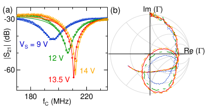
At a refrigerator temperature K, gate voltages were set to pinch off the quantum dot completely (device resistance ). The quality of the impedance match in this configuration was probed by measuring the transmission between ports 1 and 2, which is proportional to . With set to the upper end of its range ( pF), Fig. 2(a) shows as a function of frequency for different values of . As is increased, the resonance frequency increases, confirming the change in . The quality of the match depends strongly on , with a minimum in the reflected power near V. From fits to these data using a simple circuit model, parameters can be estimated as follows (see also Supplementary Information): From the trace with V, the tuned capacitances and , the effective resistance characterizing parasitic losses, and the cable insertion loss can be extracted. Traces for other values of are then well reproduced using only and as free parameters. Perfect matching is achieved at MHz and, according to this model, with pF. Using the inferred insertion loss and the known amplifier gain, which give the proportionality constant between and , the complex reflection coefficient can be plotted on a Smith chart (Fig. 2(b)). As is tuned, the traces cross the origin, confirming that the minimum seen in Fig. 2(a) indeed indicates a perfect match.
III Characterizing the capacitance sensitivity
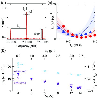
The ability to tune the circuit into perfect matching allows for highly sensitive capacitance measurements. This is demonstrated in Fig. 3, which characterizes the sensitivity by detecting the response to a known capacitance change. A sinusoidal signal with root-mean-square (RMS) amplitude and frequency 1.75 kHz was added to to modulate by a known amount (see Supplementary Information). Modulating we guarantee that the response is purely capacitive, unlike modulations on the quantum dot impedance that result in both a capacitive and a resistive response. As a result of this modulation of , the power detected at port 2 shows sidebands at (Fig. 3(a)). From the height of the sidebands above the noise floor, the sensitivity is given by , where SNR is the sideband signal-to-noise ratio expressed in dB and is the resolution bandwidth Brenning et al. (2006). Over the range of varactor settings measured, is found to change by a factor , with the best sensitivity close to perfect matching as expected (Fig. 3(b)). This dependence is reproduced well by the same circuit model as above (see Supplementary Information). In agreement with the model, is optimized when is set to the resonance frequency (Fig. 3(c)). The optimum sensitivity, attained at V and MHz, is aF.
In characterizing the sensitivity, it is crucial to take account of measurement backaction. With larger applied power or improved matching, the capacitance sensitivity can be improved at the price of a larger voltage drop across the device, potentially disturbing the state being measured. The figure of merit is therefore not simply but the product , where is the RMS excitation voltage at the device (see Supplementary Information). This is plotted in Fig. 3(b), with calculated from the carrier power using the circuit parameters from Fig. 2. For all data in Fig. 3, the carrier power at port 1 was set to dBm and near perfect matching , i.e the maximum bias applied was approximately 170 . The figure of merit is minimized at the same circuit tuning as , confirming that the optimal configuration of the circuit is indeed close to perfect matching. Note that minimizing is not achieved by minimizing , but by setting to achieve perfect matching.
IV Measuring the quantum dot impedance
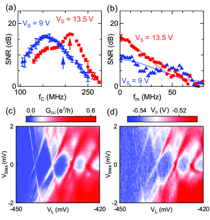
We now turn to measurements of the quantum dot. First, we confirm that the impedance of the device itself can be measured with good sensitivity and bandwidth. Gate voltages were adjusted to the flank of one Coulomb peak at a point of maximum transconductance. With a modulation voltage now applied to a gate, Fig. 4(a) shows the sideband SNR as a function of for two different varactor settings. Again, the perfect matching condition (still corresponding to =13.5 V) yields a bigger SNR. Figure 4(b) shows SNR as a function of , from which the readout bandwidth can be extracted; this is found to be 34 MHz at = 9 V and 18 MHz at =13.5 V. These data confirm that the readout bandwidth is set by the factor of the circuit, and that the tradeoff between bandwidth and sensitivity can be tuned via a varactor.
Next, the stability diagram of the quantum dot is measured (see Supplementary Information). With the circuit cooled to mK, simultaneous measurements of the DC transport conductance and the demodulated signal are shown as a function of and (Fig. 4(c) and (d)). Coulomb blockade diamonds are evident in both Fig.4(c) and (d). The similarity between these plots shows that changes in the quantum dot impedance are well captured in reflectometry. Although the setup is optimized for capacitance sensitivity measurements, we can also operate our device as a single-electron transistor and estimate its charge sensitivity. The charge sensitivity was calculated from the measured SNR at a given bandwidth and the charge modulation, estimated from the modulation amplitude and the Coulomb peak spacing Schoelkopf et al. (1998), in an analogous expression to the one used for . We obtain with a maximum of . For Si transistors, the state-of-the-art value of 37 was achieved with an applied voltage to the RF gate of 0.5 mV Gonzalez-Zalba et al. (2015). Our diminished charge sensitivity reflects the smaller RF bias, the smaller lever arm and the life time broadening of the Coulomb peaks with respect to ref. Gonzalez-Zalba et al. (2015).
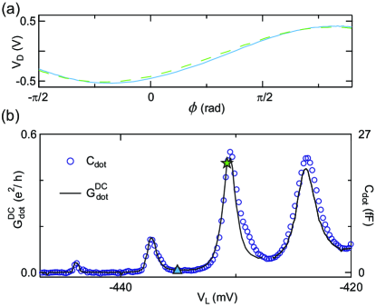
In the data of Fig. 4(d), the demodulated signal is sensitive to both conductance and capacitance of the quantum device. To isolate the capacitance , we measure as a function of the phase shift applied in the demodulation circuit. Figure 5(a) shows traces measured on and off a Coulomb peak, showing the phase shift associated with the quantum capacitance. To extract from the measured phase shift, is not sufficient simply to assume they are proportional, because changes in the quantum dot conductance also lead to a phase shift; however, using the measured DC conductance within our circuit model, it is possible to calculate (see Supplementary Information). Figure 5(b) shows calculated at each gate voltage over a series of Coulomb peaks, together with measured at the same settings.
It is evident that the quantum dot capacitance is proportional to the conductance. This reflects the fact that both quantities are proportional to the density of states of the quantum dot (see Supplementary Information). This contrasts with previous measurements where the tunnel barriers are more opaque and non-proportionality between conductance and capacitance can be observed Gabelli et al. (2006); Chorley et al. (2012). This is the case, for instance, when the quantum dot dynamics is dominated by the quantum charge relaxation effect Büttiker et al. (1993), evidenced in RF conductance measurements. This rich phenomenology Nigg et al. (2006); Hamamoto et al. (2010); Filippone et al. (2011); Cottet et al. (2015) can be explored with our setup.
V Discussion
These sensitive measurements of quantum dot impedance are promising for readout of singlet-triplet spin qubits in a double quantum dot. Using quantum capacitance for readout of a singlet-triplet obviates the need for a charge sensor Petersson et al. (2010), which is attractive for scalable two-dimensional architectures. However, although the theoretical sensitivity of this technique Johansson et al. (2006) allows for single-shot readout in a few microseconds, practical sensitivities have been found to be well below this, in part because of poor impedance matching.
Estimating the difference in quantum capacitance Petersson et al. (2010) between qubit states as fF, our measured sensitivity would at first sight indicate single-shot readout with unit SNR in integration time ns. Crucially, this sensitivity is achieved with a maximum bias , which is smaller than the typical singlet-triplet splitting in a qubit device Petta et al. (2005), and therefore does not induce charge relaxation in the triplet manifold. However, this calculation does not take into account the fact that the quantum capacitance peaks in a narrow bias range near zero detuning. The single-shot readout time should instead be estimated by comparing the product , which characterizes the sensitivity to charge induced on the source electrode, with the actual charge induced by electron tunneling, where is the lever arm. Taking from Fig. 4 and the mean value of close to perfect matching, we find that unit SNR requires . Since this is about twice the singlet-triplet qubit relaxation time Barthel et al. (2009) in GaAs, further improvements will be required to achieve single-shot readout. Our approach can be improved by optimizing remaining geometric capacitance in the circuit, by using superconducting inductors to increase the quality factor Churchill (2012); Colless et al. (2013), and by using a superconducting amplifier with drastically reduced noise temperature Stehlik et al. (2015).
VI Acknowledgements
We acknowledge discussions with M. Shea and J. Medford. Research at Oxford University was supported by EPSRC (EP/J015067/1), DSTL, the European Union, and the Royal Academy of Engineering. This publication was also made possible through support from Templeton World Charity Foundation. The opinions expressed in this publication are those of the authors and do not necessarily reflect the views of Templeton World Charity Foundation.
References
- Schoelkopf et al. (1998) R. J. Schoelkopf, P. Wahlgren, A. A. Kozhevnikov, P. Delsing, and D. E. Prober, Science 280, 1238 (1998).
- Cassidy et al. (2007) M. C. Cassidy, A. S. Dzurak, R. G. Clark, K. D. Petersson, I. Farrer, D. A. Ritchie, and C. G. Smith, Appl. Phys. Lett. 91, 222104 (2007).
- Reilly et al. (2007) D. J. Reilly, C. M. Marcus, M. P. Hanson, and A. C. Gossard, Appl. Phys. Lett. 91, 162101 (2007).
- Barthel et al. (2010) C. Barthel, M. Kjrgaard, J. Medford, M. Stopa, C. M. Marcus, M. P. Hanson, and A. C. Gossard, Phys. Rev. B 81 (2010).
- LaHaye et al. (2009) M. D. LaHaye, J. Suh, P. M. Echternach, K. C. Schwab, and M. L. Roukes, Nature 459, 960 (2009).
- Petersson et al. (2010) K. Petersson, C. Smith, D. Anderson, P. Atkinson, G. Jones, and D. Ritchie, Nano Lett. 10, 2789 (2010).
- Chorley et al. (2012) S. J. Chorley, J. Wabnig, Z. V. Penfold-Fitch, K. D. Petersson, J. Frake, C. G. Smith, and M. R. Buitelaar, Phys. Rev. Lett. 108, 036802 (2012).
- Jung et al. (2012) M. Jung, M. D. Schroer, K. D. Petersson, and J. R. Petta, Appl. Phys. Lett. 100, 253508 (2012).
- Schroer et al. (2012) M. D. Schroer, M. Jung, K. D. Petersson, and J. R. Petta, Phys. Rev. Lett. 109 (2012).
- Colless et al. (2013) J. I. Colless, A. C. Mahoney, J. M. Hornibrook, A. C. Doherty, H. Lu, A. C. Gossard, and D. J. Reilly, Phys. Rev. Lett. 110, 046805 (2013).
- Gonzalez-Zalba et al. (2015) M. F. Gonzalez-Zalba, S. Barraud, A. J. Ferguson, and A. C. Betz, Nat. Commun. 6, 6084 (2015).
- Xue et al. (2009) W. W. Xue, Z. Ji, F. Pan, J. Stettenheim, M. P. Blencowe, and A. J. Rimberg, Nat. Phys. 5, 660 (2009).
- Aassime et al. (2001) A. Aassime, G. Johansson, G. Wendin, R. Schoelkopf, and P. Delsing, Phys. Rev. Lett. 86, 3376 (2001).
- Müller et al. (2010) T. Müller, B. Küng, S. Hellmüller, P. Studerus, K. Ensslin, T. Ihn, M. Reinwald, and W. Wegscheider, Appl. Phys. Lett. 97, 202104 (2010).
- Hellmüller et al. (2012) S. Hellmüller, M. Pikulski, T. Müller, B. Küng, G. Puebla-Hellmann, A. Wallraff, M. Beck, K. Ensslin, and T. Ihn, Appl. Phys. Lett. 101, 042112 (2012).
- Pozar (2011) D. M. Pozar, Microwave Engineering (John Wiley and Sons, 2011).
- Hornibrook et al. (2014) J. M. Hornibrook, J. I. Colless, A. C. Mahoney, X. G. Croot, S. Blanvillain, H. Lu, A. C. Gossard, and D. J. Reilly, Appl. Phys. Lett. 104, 103108 (2014).
- Mavalankar et al. (2013) A. Mavalankar, S. J. Chorley, J. Griffiths, G. A. C. Jones, I. Farrer, D. A. Ritchie, and C. G. Smith, Appl. Phys. Lett. 103, 133116 (2013).
- Brenning et al. (2006) H. Brenning, S. Kafanov, T. Duty, S. Kubatkin, and P. Delsing, J. Appl. Phys. 100, 114321 (2006).
- Gabelli et al. (2006) J. Gabelli, G. Fève, J. Berroir, B. Plaçais, A. Cavanna, B. Etienne, Y. Jin, and D. C. Glattli, Science 313, 499 (2006).
- Büttiker et al. (1993) M. Büttiker, H. Thomas, and A. Prêtre, Phys. Lett. A 180, 364 (1993).
- Nigg et al. (2006) S. E. Nigg, R. López, and M. Büttiker, Phys. Rev. Lett. 97 (2006).
- Hamamoto et al. (2010) Y. Hamamoto, T. Jonckheere, T. Kato, and T. Martin, Phys. Rev. B 81 (2010).
- Filippone et al. (2011) M. Filippone, K. Le Hur, and C. Mora, Phys. Rev. Lett. 107 (2011).
- Cottet et al. (2015) A. Cottet, T. Kontos, and B. Douçot, Phys. Rev. B 91, 205417 (2015).
- Johansson et al. (2006) G. Johansson, L. Tornberg, and C. M. Wilson, Phys. Rev. B 74, 100504 (2006).
- Petta et al. (2005) J. Petta, A. C. Johnson, J. Taylor, E. Laird, A. Yacoby, M. D. Lukin, C. Marcus, M. Hanson, and A. Gossard, Science 309, 2180 (2005).
- Barthel et al. (2009) C. Barthel, D. J. Reilly, C. M. Marcus, M. P. Hanson, and A. C. Gossard, Phys. Rev. Lett. 103 (2009).
- Churchill (2012) H. O. H. Churchill, PhD Thesis, Harvard University (2012).
- Stehlik et al. (2015) J. Stehlik, Y.-Y. Liu, C. M. Quintana, C. Eichler, T. R. Hartke, and J. R. Petta, Phys. Rev. Appl. 4 (2015).