A linear-scaling source-sink algorithm for simulating time-resolved quantum transport and superconductivity
Abstract
We report on a “source-sink” algorithm which allows one to calculate time-resolved physical quantities from a general nanoelectronic quantum system (described by an arbitrary time-dependent quadratic Hamiltonian) connected to infinite electrodes. Although mathematically equivalent to the non equilibrium Green’s function formalism, the approach is based on the scattering wave functions of the system. It amounts to solving a set of generalized Schrödinger equations which include an additional “source” term (coming from the time dependent perturbation) and an absorbing “sink” term (the electrodes). The algorithm execution time scales linearly with both system size and simulation time allowing one to simulate large systems (currently around degrees of freedom) and/or large times (currently around times the smallest time scale of the system). As an application we calculate the current-voltage characteristics of a Josephson junction for both short and long junctions, and recover the multiple Andreev reflexion (MAR) physics. We also discuss two intrinsically time-dependent situations: the relaxation time of a Josephson junction after a quench of the voltage bias, and the propagation of voltage pulses through a Josephson junction. In the case of a ballistic, long Josephson junction, we predict that a fast voltage pulse creates an oscillatory current whose frequency is controlled by the Thouless energy of the normal part. A similar effect is found for short junctions; a voltage pulse produces an oscillating current which, in the absence of electromagnetic environment, does not relax.
As quantum nanoelectronics experiments get faster (in the GHz range and above) it becomes possible to study the time dependent dynamics of devices in their quantum regimes, i.e. at frequencies higher than the system temperature (K corresponds roughly to GHz). Recent achievements include coherent single electron sources with well defined release timeDubois et al. (2013) or energyFève et al. (2007), pulse propagation along quantum Hall edge statesAshoori et al. (1992); Kamata et al. (2010); Kumada et al. (2011) and terahertz measurements in carbon nanotubesZhong et al. (2008). While the mathematical framework for describing quantum transport in the time domain has been around since the 90s Wingreen et al. (1993); Jauho et al. (1994), the corresponding non-equilibrium Green’s function formalism (NEGF) is rather cumbersome and can only be solved in rather simple situations, even with the help of numerics. In Ref. Gaury et al., 2014a we developed an alternative formulation of the theory which is much easier to solve numerically, in addition to being more physically transparent. The approach of Ref. Gaury et al., 2014a (to which we refer for further references) was recently used in a variety of situations including electronic interferometersGaury and Waintal (2014); Gaury et al. (2015), quantum Hall effectGaury et al. (2014b), normal-superconducting junctionsWeston et al. (2015), Floquet topological insulatorsFruchart et al. (2016) and the calculation of the quantum noise of voltage pulsesGaury and Waintal (2016).
The best algorithm introduced in Ref. Gaury et al., 2014a (nicknamed WF-C) has a computational execution time that scales linearly with the system size , but as the square of the total simulation time. While for ballistic systems this limitation was not too stringent, in situations with large separations of time scales (such as the Josephson junctions studied below), it makes the numerical calculation computationally prohibitive. In this manuscript, we present an extension of the previous approach which reduces the computational complexity down to . This is achieved with the addition of non-hermitian terms, referred to as “sink” terms, in the Hamiltonian in addition to the “source” terms introduced in the WF-C method of Ref. Gaury et al., 2014a. The new technique remains mathematically equivalent to the NEGF formalism.
This articles is organized as follows. Section I introduces a general class of models and the time dependent scattering states of the system. In section II we briefly recall how a simple change of variables leads to the introduction of an additional source term in the Schrödinger equation, which greatly facilitates the numerical treatment. In section III we develop the new part of the algorithm and show how the introduction of sink terms solves previous difficulties at long times. Finally, section IV discusses applications to the physics of out of equilibrium Josephson junctions. After recovering well known effects (Multiple Andreev Reflection in both short and long junctions, AC Josephson effect, relaxation of Andreev bound states), we study the propagation of fast voltage pulses through Josephson junctions.
I Model
We consider a general class of models describing a quantum device of finite extent attached to semi-infinite electrodes. The full system is described by a general quadratic Hamiltonian of the form
| (1) |
where () are the Fermionic creation (annihilation) operators of a one-particle state on site . A “site” typically labels position as well as other degrees of freedom such as spin, orbital angular momentum or electron/hole (as in the superconducting application below). The are the matrix elements of the Hamiltonian matrix . The system consists of a time-dependent central region connected to several leads as depicted in Fig. 1. We keep the Hamiltonian of the central region fully general but restrict the leads to be semi-infinite, time independent and invariant by translation (i.e. they have a quasi-one dimensional periodic structure). Each lead remains in its thermal equilibrium at all times. We further suppose that the time-dependent perturbations are only switched on at positive times, so that . Note that if one has a uniform time-varying potential in one or more of the leads then a gauge transformation can always be performed such that the time-dependence is brought into the interface between the lead and the central region, which can then be included in the definition of the central region. Typically the time dependent part of the Hamiltonian is restricted to rather small regions as illustrated in Fig. 1.
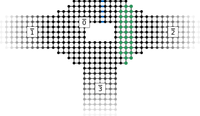
Before the time-dependent perturbations are switched on, the system is characterized by its scattering wavefunctions that are labeled by their energy and incoming channel ,
| (2) |
The scattering states are standard object of mesoscopic physics and can be obtained directly by wave matching the incoming and outgoing modes at the lead-system boundary. For complicated geometries these can be obtained numerically by using e.g. the Kwant packageGroth et al. (2014). A physical observable (e.g. electronic density or local currents) can be directly obtained from the knowledge of these wavefunctions by simply filling up the one-body scattering states according to Fermi statistics, using
| (3) |
where is the Fermi function of the electrode associated with channel . The celebrated Landauer formula for the conductance is a special case of Eq.(3).
The generalization of Eq.(3) to the time-dependent problem is rather straightforward: one first obtains the scattering states and lets them evolve according to the Schrödinger equation
| (4) |
with the initial condition . The observables follow from Eq.(3) where the are replaced by :
| (5) |
The fact that such a scheme is equivalent to the NEGF formalism or to the scattering approach was derived in Ref. Gaury et al., 2014a. In particular, the central objects of the NEGF formalism, the so-called lesser (), greater () and retarded () Green’s functions, have simple expressions in term of the time dependent scattering states,
Note that in the presence of bound states (such as the Andreev states in the Josephson junctions described below) the above integral need to be replaced by an integral over the continuum plus a sum over the bound states, as explained in Ref. Profumo et al., 2015.
II The source
In its original form, Eq.(4) is not very useful for numerics because the wave function spreads over the entire infinite system. A first simple, yet crucial, step consists in introducing the deviation from the stationary solution, ,
| (9) |
satisfies,
| (10) |
with
| (11) |
and
| (12) |
The new “source” term can be computed from the knowledge of the stationary scattering states and is localized at the place where the time-dependent perturbation takes place (where , typically the colored regions of Fig. 1). Eq. (10) is already much better than Eq. (4) for numerics because the initial condition corresponds to a wavefunction that vanishes everywhere. One can therefore truncate Eq. (10) and keep a finite system around the central time-dependent region where the source term lies. In practice, one adds layers of each electrodes. Note that in order for this procedure to be correct, the stationary scattering states are calculated for the infinite system and the truncation is only performed afterwards. For the truncation to be valid, the size of this finite region must be larger than where is the maximum group velocity at which the wavefunction can propagate and the duration of the simulation. Hence, for large values of , the total computational time to integrate Eq. (4) scales as . This algorithm corresponds to the WF-C algorithm of Ref. Gaury et al., 2014a. Here, we have explicitly removed a factor from the definition of compared to Ref. Gaury et al., 2014a. This change, while small, leads to an improve stability of the numerical integration: the equation of motion for does not have an (potentially fast) oscillating factor in the source term. This means that the numerical integration scheme used for solving eq. (10) is now limited by the intrinsic timescales of the problem, and not the “artificial” timescale introduced by a bad choice of gauge.
III The sink
The scaling of the algorithm comes from the fact that for long simulation times, one needs to introduce large part of the leads () in order to avoid spurious reflections at the boundaries where the leads have been truncated. To proceed, one needs to take advantage of the special structure of the leads: they are not only time-independent, but also invariant by translation. Hence whatever enters into the lead will propagate toward infinity and never come back to the central region. Mathematically, the form of in the leads is a superposition of outgoing plane waves Gaury et al. (2014a)
| (13) |
where and are related by the dispersion relation of the lead, indexes the different unit cells in the lead, the transverse wavefunction of the corresponding mode and is the time-dependent part of the inelastic scattering matrix. The crucial point of Eq.(13) is that it only contains outgoing modes as the incoming one has been subtracted when removing the stationary scattering state. Therefore, once the wave function starts to reach the leads, it propagates toward infinity and never comes back to the central system.
A natural idea that comes to mind is to replace the finite fraction of the electrodes by some sort of (non-hermitian) term in the Hamiltonian that “absorbs” the wavefunction that enters the leads. This has been studied in the literature in the context of various partial differential equations,Antoine et al. (2008); Muga et al. (2004); Shemer et al. (2005); Riss and Meyer (1998, 1995); Kalita and Gupta (2011); Ge and Zhang (1998) and is usually known as a complex absorbing potential. The difficulty lies in the fact that this absorbing term must not give rise to reflections. At a given energy, a perfectly absorbing boundary condition does exist, it corresponds to adding the self energy of the lead at the boundary (which is a non-local complex absorbing potential, see WF-D method of Ref. Gaury et al., 2014a). However the outgoing waves of Eq.(13) span a finite energy window so that some energies would get reflected back to the central region. One solution to obtain a perfectly absorbing boundary condition is to use a boundary condition that is non local in timeAntoine et al. (2008), as in the WF-B method of Ref. Gaury et al., 2014a; this leads to algorithms that scale as .
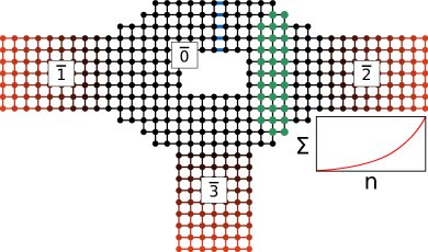
We choose instead to design an imaginary potential that varies spatially. We show that for any desired accuracy, we can design an imaginary potential that spreads over a finite width of electrode unit cells - where depends only of the required accuracy, not on . In practice, this new algorithm is much more effective than WF-C when becomes larger than the ballistic time of flight through the system. The idea behind the algorithm is fairly straightforward: suppose that a plane wave with a dispersion relation propagates inside one electrode. If one adds an imaginary potential to the Schrödinger equation, this plane wave becomes evanescent which eventually leads to the absorption of the wave. On the other hand, any abrupt variation of potential (or in this case of imaginary potential) leads to unwanted reflection back to the central part of the system. Hence, the algorithm consists in adiabatically switching on the imaginary potential inside a finite fraction of the electrode, see Fig. 2 for a sketch. The new equation of motion contains both the previous source term and the additional sink in the electrodes,
| (14) |
where the matrix is diagonal and vanished in the central region while it reads
| (15) |
in the absorbing layer placed at the beginning of the electrodes. The index labels the unit cells of the leads and is the identity matrix defined over a unit cell. What remains to be done is to specify the function so that it is large enough to absorb all waves entering into the lead while being smooth enough not to produce spurious reflections. The error induced by the boundary conditions must not exceed a tolerance . Our aim is to minimize the number of layers that must be added in the simulation to absorb the outgoing waves without the error exceeding .
III.1 Analytical Calculation of the spurious reflection
Before we can design a suitable imaginary potential, we must understand how the spurious reflection back to the central part depends on the shape of . We will start from a continuum model in order to develop an analytical solution for this simple case. The rationale, other than its tractability, is the fact that spurious reflections happen when varies on a spatial scale that is short compared to the wavelength of the solution, hence is dominated by small momentum where the tight-binding dispersion relation reduces to its continuum limit. We will show that there is an extremely good agreement between the analytical results derived in this section and numerical calculations of the discretized model.
Let us consider the stationary 1D Schrödinger equation,
| (16) |
where is the electron effective mass and we have introduced a length scale, , which controls how fast varies. For negative , we set so that the wave function is in a superposition of plane waves,
| (17) |
where we define . Our goal is to calculate the spurious reflection probability induced by the presence of the imaginary potential. We first rescale the equation by and define , and to obtain the dimensionless equation,
| (18) |
with
| (19) |
for . It is apparent from Eq.(18) that the spurious reflection is controlled by the dimensionless parameter . Since we want this spurious reflection to be small, we will work in the limit of large and expand in powers of . The zeroth order contribution is simply the extension of the WKB limit to imaginary potential; the wave function takes the form of an evanescent wave,
| (20) |
with satisfying
| (21) |
where primes denote derivatives. We expand to first order in , and apply the boundary condition Eq. (19) at , as well as (perfect reflection at a the end of the simulation domain at ) to obtain the zeroth order contribution to :
| (22) |
where
| (23) |
is independent of . Physically speaking, the wave function is exponentially attenuated up to the hard wall at where it is fully reflected and then again exponentially attenuated until .
The contribution takes into account the finite absorption due to the imaginary potential but not the spurious reflections due to wavevector mismatch. It it therefore necessary to go beyond the adiabatic WKB approximation and calculate its deviation . We can ignore the hard wall at as it will play no role in what follows. Generalizing the WKB approximation we choose the following ansatz for :
| (24) |
contains the fast oscillating and decaying parts, while contains the remaining (slow) parts. Plugging the ansatz Eq. (24) into Eq. (18) our Schrödinger equation becomes
| (25) | ||||
with
| (26) |
We write as and notice that, in the limit , Eq. (25) admits a solution . In this limit there should be no backscattering from the imaginary potential, so and , to match the boundary conditions Eq. (19). The derivatives of hence vanish and we arrive at
| (27) |
up to terms of order . Eq.(27) can be solved by the variation of constant method,
| (28) |
with
| (29) |
Applying the continuity condition on and at we obtain the order contribution to the reflection amplitude:
| (30) |
which we can write explicitly, using Eq. (29) and the condition , as
| (31) |
One can understand as the Fourier transform at (large) frequency () of the gradient of the imaginary potential weighted by the absorption that has already taken place. Putting together Eq. (22) and Eq. (31), we finally obtain
| (32) | ||||
Eq.(32) is the main result of this section. Now that we understand how the spurious reflection depends on the shape of , we need to design the imaginary potential so as to minimize Eq.(32) (for a given ). More precisely, for a given required precision , we wish to enforce irrespective of the value of the energy . Such a stringent condition is not, strictly speaking, feasible as when (all the variations of the imaginary potential become “abrupt” when the electronic wave length becomes infinite) but we will see that the associated error can be kept under control.
A shape that keeps small must be initially very flat and later (when a significant fraction of the wave has been already absorbed) can increase more rapidly. We leave a full optimization of this shape for future study and focus on an algebraic one,
| (33) |
from which the reflection amplitude calculated from Eq. (32) reads,
| (34) |
As a consistency check of the approach developed above, we compare this analytical result for the reflection probability with direct numerical calculation using the kwant d.c transport package Groth et al. (2014). To do so we discretize the continuous Schrödinger equation onto a lattice of lattice spacing 1. Figure 3 shows how scales for the case and , showing an excellent agreement between the direct numerical simulations and the above analytical result in the limit of validity of the latter (small reflection). Figure 3c shows that the reflection has a minimum as a function of which corresponds to a compromise between the first and last term of Eq. (34). Once has been chosen large enough for the first term of Eq. (34) to be negligeable, one can always choose large enough to control the second term. We can already anticipate that the difficulties will come from vanishing energies for which the spurious reflection goes toward unity.

III.2 Numerical precision in the time domain
Now that we understand the d.c. case, let us consider the previous one dimensional model in the time domain and send a Gaussian voltage pulse through the wire. This problem has been studied in detailed in Ref. Gaury et al., 2014a to which we refer for more details. We compute the current flowing and measure the error with respect to a reference calculation ,
| (35) |
where is the time-dependent probability current for a particle injected at energy using the above designed imaginary potential to absorb the outgoing waves. The reference calculation is performed without imaginary potential, but with enough added unit cells in the leads such that the solution does not have time to propagate back into the central region before the end of the simulation; this corresponds to the WF-C method of Ref. Gaury et al., 2014a.
Figure 4a shows the scaling of the error in the time-dependent calculation with respect to the d.c. reflection probability of the absorbing region as is changed. The current at an energy at the centre of the spectrum is calculated. We see from figure 4 that for very short absorbing regions the error scales proportionally to , whereas for longer regions it scales as . This simply reflects the fact that the error on is proportional to : since the current (hence ) is quadratic in , the error has the form . More importantly, we see that we can control the error of the calculation with arbitrary precision and for extremely long times (we checked this last point for much longer times than what is shown in the inset).
More interesting is the behavior of the error as a function of the injection energy . Indeed, since there are large spurious reflections when , we might expect to behave badly as one decreases the energy. Figure 4b indeed shows that the error increases as the energy is lowered. However, one finds that saturates at small energy. Furthermore, the saturated valued decreases with and can thus be controlled. This behaviour comes from the structure of the wave function as shown in Eq.(13); even though one injects an electron at a definite energy inside the system, the energy of the outgoing wave is ill defined. The contribution to the wavefunction coming from spurious reflections takes the form
| (36) |
The contribution spreads over an energy window which characterizes the inelastic scattering matrix, . typically decays on an energy scale of the order of (see Fig. 10 of Ref. Gaury et al., 2014a for an example). For the voltage pulse considered here (which sends one electron through the system), is essentially the duration of the pulse. The consequence is that the reflection is averaged over an energy window of width , which blurs the behaviour of :
| (37) |
We conclude that the error can always be made arbitrarily small, irrespective of the duration of the simulation. A slight drawback is that for a given imaginary potential, the precision of the calculation can depend on the actual physics taking place inside the central system (which sets ) if one injects electrons with energies close to the band edges of the leads.

III.3 A general algorithm
We now discuss how to turn the above results into a practical scheme to perform numerical calculations in a robust way.
Since we cannot guarantee the error for a given shape of the imaginary potential (we have seen above that it might depend on the physics of the central region), we first need to design an algorithm for an on-fly calculation of an error estimate (without the reference calculation used above). This can be done as follow for a small additional computational cost. In the integration of the Schrödinger equation, one separates the wave function in the central region and in the leads (let us suppose that there is only one lead for simplicity). The equations to be integrated take the block form,
| (38) | |||||
| (39) |
where is the source term present in the central region and the imaginary potential is included in . One then introduces a second “copy” of the lead wave function that uses a different imaginary potential . The equations of motion for this “copy” are
| (40) |
One then keeps track of both and simultaneously, although only will affect the dynamics of . The trick is to design , i.e. to insert extra lead layers before the imaginary potential, and to monitor the difference between and in the lead cell adjacent to the central region, . Spurious reflections from the presence of will arrive at the boundary of the central region for before , as the latter has extra lead layers. This delay in the arrival of the spurious reflections will give rise to a finite . Note that will remain 0 in the case that there are no spurious reflections. can thus be used as an error estimate for the wavefunction in the lead.
In the worst case scenario this scheme will increase the computational cost by a factor of 2 (when the absorbing region represents the largest part of the system). It is worth noting, however, that without an error estimate for the spurious reflections one would have to check for convergence of results by performing several simulations with different values of , the absorbing region length.
The remaining task is to choose the parameters and for a given shape of the imaginary potential. Ideally we would choose as small as possible so as to minimize the extra computational effort while requiring that remain smaller than a fixed maximum error, . Given it is easy to choose such that the first term in Eq. (34) is not a limitation. By noting that ( is the lead bandwidth and is the discretization step) we see that it is sufficient to choose such that for the absorption process not to be the limiting factor of the precision. Next, one needs to choose large enough to enforce . In practice, we found that a few hundred (up to a thousand) lead cells is almost always sufficient for the physics we have studied so far, for typical .
Let us end with a last point of practical importance. We have seen that the major contribution to spurious reflection comes from a narrow region around the band edge of the lead. The wavefunctions associated with these energies propagate extremely slowly into the absorbing region due to the vanishing velocity at the band edge. Unless one is interested in extremely long simulation times, we can take advantage of this by placing a small number of lead layers before the imaginary potential. The slow-moving waves will induce spurious reflections, but will take a long time to traverse this buffer layer due to their small group velocity. Meanwhile the absorbing region does not have to be made as long, as it does not have to absorb waves of vanishingly small energy.
IV Voltage pulses in long Josephson Junctions
We are now in possession of a robust algorithm to simulate time-dependent open systems. Compared with our own previous approach, the computing time is now . This new algorithm allows us to treat cases where very small energies (hence large times) come into play. We now turn to a specific application concerning superconducting - normal - superconducting Josephson junctions where the large separation of scales (: Thouless energy, : superconducting gap, : Fermi energy) makes a linear scaling algorithm very welcome. An interesting aspect of superconductivity is that the problem is intrinsically time dependent even in d.c. as soon as there are voltage differences across the superconductors (as evidenced by the a.c. Josephson effect which transforms a d.c. voltage into an a.c. current). We emphasize that the algorithm is in no way limited to superconductivity and refer to the introduction for other applications (such as quantum Hall effect, graphene…)
In the following, we will focus on 3 physical effects. First we will recover known physics of Josephson junctions: the Multiple Andreev Reflection (MAR) phenomena and the a.c. Josephson effect. Second, we will discuss the relaxation of a SNS junction after an abrupt raise of the applied potential, showing how MAR comes into play in the relaxation rate. Third, we will study a novel phenomenon, the propagation of a voltage pulse through a Josephson junction.
IV.1 Minimum microscopic model for a SNS junction
We consider voltage-biased Josephson junctions. In this setup we have two infinite superconducting reservoirs coupled by a normal region of length . We shall treat the problem using a 1D Bogoliubov-De-Gennes Hamiltoniande Gennes (1966):
| (41) |
where , and is an operator which annihilates an electron at position in a spin up state. is the superconducting order parameter, which reads,
| (42) |
with and is the voltage bias applied to the left superconductor (which is 0 before ). Likewise, the electrical-chemical potential reads,
| (43) |
where is the Fermi energy and a potential barrier. We only consider a single spin sector as our model is spin independent; the two spin sectors give degenerate solutions.
In order to put eq. (41) into a form where we can apply the algorithm developed above we first apply a gauge transformation
| (44) |
where are Pauli matrices and is the Heaviside function. This transformation brings all the time-dependence for into a time-dependence in the momentum term at , the boundary between the left superconductor and the normal region. In this gauge both superconductors are at equilibrium. We next discretize onto a lattice with spacing , using a central difference approximation for the second spatial derivative, , to obtain a tight-binding model:
| (45) |
with the matrices being non-zero only for diagonal and nearest-neighbour matrix elements,
| (46) |
| (47) |
| (48) |
where (and , its Hermitian conjugate) are vectors of creation (annihilation) operators at site . is the Kronecker delta and is a discrete Heaviside function, defined as 1 if and 0 otherwise. is the potential barrier. This model can be readily solved numerically using the above-developed technique.
IV.2 Multiple Andreev Reflection and a.c. Josephson Effect
Let us now apply our numerical technique and discuss the physics of a voltage biased Josephson junction. There are two very different regimes to discuss: at low voltage one observes the a.c. Josephson effect, while at higher voltage one observes multiple Andreev reflections (MAR). Both effects are closely related, as the Josephson effect corresponds to the limit of an infinite number of Andreev reflections, yet they are usually calculated with different techniques. Indeed, one of the challenges of such a simulation is that to access small bias voltages one needs to go to very long times . For this problem the source-sink algorithm thus has a distinct advantage over previous methods due to its linear scaling with simulation time.
In this subsection, we concentrate on a short junction and add a potential barrier that allows us to tune the transmission probability of the normal part of the junction from insulating to ballistic . To obtain a current-voltage characteristic for the junction we perform a separate simulation for each value of voltage required. For a given simulation (voltage value) we use the following protocol. At the voltage of the left superconductor is raised smoothly, , until , when is held at a value (we used ). The system relaxes to a steady state and we can obtain the current using eq. (5). The d.c. current can then be obtained by taking an average over one period of the fully time-dependent current after the system has reached a steady state.
Let us start with the a.c. Josephson effect. At equilibrium, the ground state energy of the junction depends on the phase difference between the order parameters of the two superconductors. The corresponding supercurrent is given by
| (49) |
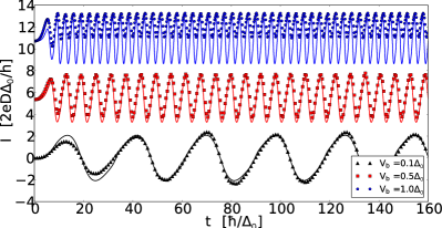
When a small bias is applied to the junction, increases linearly in time and one observes the a.c. Josephson effect at frequency . This is perhaps the most striking manifestation of superconductivity; a d.c. bias leads to an a.c. effect. Figure 5 shows a numerical calculation of the current as a function of time together with the adiabatic prediction discussed above (the dispersion relation was calculated from the equilibrium junction and differentiated numerically). We see a perfect agreement at low bias, indicating that our technique can reach the adiabatic limit. Upon increasing the bias, one leaves the adiabatic limit and the corresponding prediction becomes less accurate.
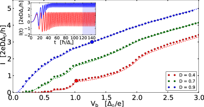
Indeed, as one increases the bias, a d.c. component starts to appear in the current. This is best understood starting from large bias. For , the charges can flow directly from the left “valence” band of the superconductor to the right “conduction” band (using the semiconductor terminology). As one lowers the bias, this direct process is no longer possible and at least one Andreev reflection takes place on the right superconductor. As one further lowers the bias, more and more Andreev reflections are needed and one observes kink in the I-V characteristics at values with The Fourier components of the MAR current have been previously calculated using a Floquet approachAverin and Bardas (1995); Cuevas et al. (1996) and are routinely observed experimentally (see for instance Ref. Scheer et al., 1997). Here we recover those results using a microscopic model for the junction. Figure 6 compares the current-voltage characteristics of such a junction calculated in Ref. Averin and Bardas, 1995 with a simulation using the source-sink algorithm for different values of the transmission () of the junction. We see a very good agreement with these previous results.
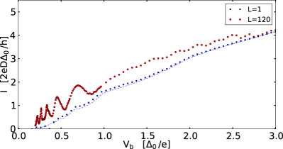
Using the source-sink algorithm we can go beyond the limitations of an analytical approach for little extra overhead. We can, for example, explore the behaviour of a long Josephson junction under voltage bias. Figure 7 compares the current-voltage characteristics of a long junction with the short junction studied previously. We clearly see that the long junction has more sub-gap features, which can be attributed to the larger number of Andreev states below the gap. We see that numerics has an advantage over analytical approaches in this regard, in that it is relatively cheap to explore new regions of parameter space or in crossover regions between tractable limits (e.g. short junction vs. long junction).
IV.3 Relaxation of Andreev bound states
An important difference of Josephson junctions with respect to other nanoelectronics systems is the presence of (so called Andreev) bound states. Since Andreev states have their energies inside the superconducting gap, there is no continuum band with which they can hybridize so that they have infinite lifetime. These states must be added explicitly in Eq. (5) and the definitions of the Green’s function (see section IV of Ref. Profumo et al., 2015 for a discussion). As the Andreev states carry the Josephson current, their role is particularly important and they cannot be ignored. This is in contrast to many non-superconducting systems where the bound states do not contribute to transport.
Andreev states give us another opportunity to study MAR physics. Suppose that we abruptly raise the voltage bias at , thereby placing the system in a non equilibrium state. Just after the voltage raise, a given wavefunction can be decomposed on the eigenbasis of the equilibrium SNS junction,
| (50) |
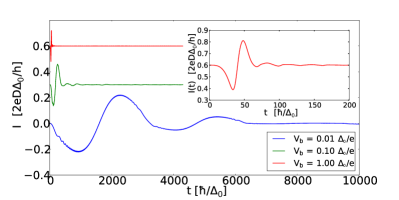
where and are respectively the projection of the wave function on the scattering states and the bound states (). It is important to realize that in the absence of bias voltage, the bound state part of the wave function will never relax (within the above model) as the Andreev states are true bound states with energy : the second part of the wave function will simply oscillate as for ever. However, the presence of the bias voltage allows the energy to change by in between two Andreev reflections so that after reflections, one can reach energies outside the gap and the wavefunction can relax. Denoting the time of flight between two Andreev reflections, we expect the relaxation time of the system to behave as .
Figure 8 shows the contribution of the Andreev bound states to the current as a function of time for three values of the bias voltage. We indeed see that the current carried by the bound states dies away with time in presence of a finite bias. Although we did not try to define precisely, we clearly see that dividing by a factor 10 leads to a 10 time increase of the relaxation time, establishing the relation which originates from the MAR assisted relaxation process.
From a numerical perspective, we note that these simulations are taken to extremely long times, in units of the inverse hopping parameter, , of the model (we chose for the above calculations). This calculation clearly necessitates the source-sink algorithm; we used an imaginary absorbing potential of order with 1000 lead cells forming the absorbing layer.
IV.4 Propagation of a voltage pulse through a Josephson junction
A natural consequence of the above discussion is that if one sends a fast voltage pulse through the system (i.e. the final bias voltage vanishes instead of having a finite value), then the corresponding bound state contribution will not relax and will oscillate for ever (within the assumptions of our model).
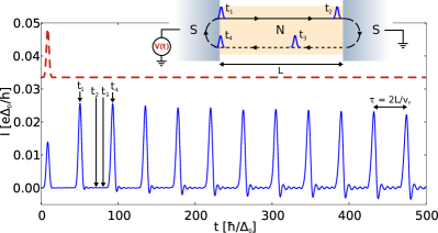
Let us study the corresponding protocol. We consider a perfectly transparent junction with a finite width, and apply a Gaussian voltage pulse of duration on the left superconducting contact. The junction has a length such that the time of flight is . We consider a “long” junction, such that . We further consider fast pulses with ( in our case). The case of slow pulses is trivial as the physics is essentially given by the adiabatic limit. The physics of fast pulses is simple yet rather interesting. The pulse generates an electron-like excitation that propagates through the system until it reaches the right superconductor. There, it is Andreev reflected as a hole-like excitation and a Cooper pair is generated in the right electrode. The excitation now propagates backward towards the left superconducting electrode where it is Andreev reflected a second time (and a Cooper pair is absorbed from the electrode). The excitation then continues its propagation again to the right. Within the above model, nothing stops this process and the excitation continues to oscillate back and forth for ever. This is rather appealing: one sends a short voltage pulse and gets an oscillating current at frequency . Beyond the current model, the relaxation time of the system will be given by the fluctuations of the voltage due to the electromagnetic environment and we anticipate a relaxation of the current on a scale given by the corresponding time.
Figure 9 shows a numerical simulation of the propagation of a voltage pulse as discussed above. Despite the fact that there is only a single voltage pulse at the start, we see pulses of current every . We do not observe any quasiparticle current in the superconducting lead; this (super)current is purely associated with the Andreev reflection process described above.
We can go a little bit further and look at the structure of the bound states that carry the supercurrent. They are given by the stationary conditionWeston et al. (2015); Mi et al. (2013); Beenakker (1992),
| (51) |
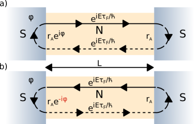
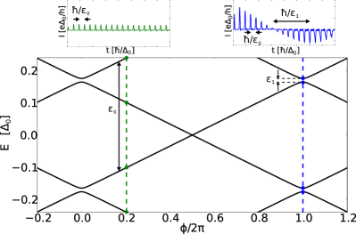
where left-hand superconductor is at a phase bias compared to the right-hand one and is the Andreev reflection amplitude for a particle incident on the superconductor at energy . The paths contributing to this amplitude are sketched in Fig. 10a. A similar expression exists for the reversed paths where the sign of is flipped; this is sketched in Fig. 10b. For we have , and we can re-write this condition as
| (52) |
In the long junction limit () close to zero energy this simplifies to:
| (53) |
which corresponds to two set of equidistant energies separated by , one set that has energy increasing with , and the other decreasing with . Each of these sets corresponds to a ballistic propagation in the continuum limit . The numerical spectrum, which is shown in Fig. 11, adheres to the above-derived result except near the degeneracy points. The degeneracies are lifted due to the finite ratio used in the numerical calculation, which induces a finite normal reflection at the normal-superconducting interfaces. The two insets of Fig. 11 show two time dependent simulation at two different values of the superconducting phase difference after the pulse, . We see that when the two sets of bound states are very close in energy the output current beats with a frequency which is given by the level spacing. For well-spaced bound states this frequency is so high that it has no visible effect on the current trace.
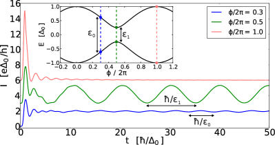
The above effect is intriguing, but unfortunately long ballistic Josephson junctions are difficult to realize experimentally (with the exception perhaps of carbon nanotubes). In diffusive junctions there will be a distribution of times of flight which will wash out the above effect. An alternative is to consider the limit of short junctions, which have been studied extensively experimentally with atomic contacts (break junctions)Scheer et al. (1997). We shall, therefore, now explore the effect of a voltage pulse applied to a short Josephson junction. We do not expect to be able to see a train of well-resolved peaks of current, as in the long junction case, because the time of flight of the short junction is much shorter than the typical pulse duration. We do, however, expect to see the effect that gives rise to the “beating” in Fig. 11, as this is governed only by the energy difference between the Andreev bound states in the junction. Figure 12 shows the current passing through a short junction when voltage pulses of varying heights are applied. We see an initial transient part followed by an oscillatory part that continues indefinitely. Initially, all the states up to are filled (Pauli principle). The pulse excites some quasiparticles into states at and also shifts the phase bias across the junction so that we are at a different place in the phase-energy plot than we were before the pulse (indicated by dashed lines in the inset to Fig. 12). Any quasiparticles in continuum states escape into the leads after some time ( in Fig. 12), however the contribution in the Andreev bound states cannot escape. After we have reached steady state we are essentially in a superposition of Andreev bound states at energy and . These two contributions interfere with one another to give a current that oscillates in time at an angular frequency . This effect is most strongly seen for , as the Andreev levels have the smallest energy gap here. For the oscillations die away with time, as the Andreev levels hybridize with the continuum at this point. By tuning the energy gap between the Andreev levels after the pulse we are able to control the frequency of the current. We can tune the energy gap by placing ourselves at different points in the phase-energy diagram (by sending in pulses of different heights), or by tuning the transparency of the junction to modify the phase-energy diagram itself.
The above calculations have been performed in absence of electromagnetic environment. The closest experimental situation that would correspond to these calculations is a Josephson junction embedded in a superconducting ring where the voltage pulse is applied through a pulse of magnetic field through the ring and the signal detected through the magnetization generated by the oscillating circulating current. A simpler configuration would involve a SQUID where one of the two junction is an atomic one and the other a regular large tunnel junction. In a SQUID setup, however, the effect of the electromagnetic environment would have to be properly included.
V Conclusion
We have developed an algorithm for simulating time-resolved quantum transport, which we dub “source-sink” due to the characteristic addition of both “source” and “sink” terms to the Schrödinger-like equations used. We demonstrated that the accuracy of the method can be tuned at the cost of increasing the runtime, and that for a given accuracy the algorithm scales linearly with the system size and the maximum time required. We confirmed the accuracy of the method by comparing our results for a Josephson junction at finite bias with analytical results from the literature.
We then studied the effect of a single voltage pulse on a (long or short) Josephson junction. We found that a single voltage pulse results in a periodic resultant supercurrent. The (rightly) controversial yet appealing concept of time crystal was recently put forward.Wilczek (2012) In analogy with a regular crystal where translational spatial symmetry is spontaneously broken, a time crystal would spontaneously break translational time symmetry. While the above effect is not a time crystal (the system in the normal part is not in its ground state), it might be as close as one can get; the superconducting ring remains in its ground state, yet a time dependent current flows through it.
In contrast to other universal effects associated to Josephson physics, the period is given here by the normal part of the device. In the absence of electromagnetic environment, the periodic current continue for ever. A precise calculation of the effect of the dissipative electromagnetic environment to damp the oscillating current is left for future work.
Acknowledgments. This work is funded by the ERC consolidator grant MesoQMC.
References
- Dubois et al. (2013) J. Dubois, T. Jullien, F. Portier, P. Roche, A. Cavanna, Y. Jin, W. Wegscheider, P. Roulleau, and D. C. Glattli, Nature 502, 659 (2013).
- Fève et al. (2007) G. Fève, A. Mahé, J.-M. Berroir, T. Kontos, B. Plaçais, D. C. Glattli, A. Cavanna, B. Etienne, and Y. Jin, Science 316, 1169 (2007).
- Ashoori et al. (1992) R. C. Ashoori, H. L. Stormer, L. N. Pfeiffer, K. W. Baldwin, and K. West, Phys. Rev. B 45, 3894 (1992).
- Kamata et al. (2010) H. Kamata, T. Ota, K. Muraki, and T. Fujisawa, Phys. Rev. B 81, 085329 (2010).
- Kumada et al. (2011) N. Kumada, H. Kamata, and T. Fujisawa, Phys. Rev. B 84, 045314 (2011).
- Zhong et al. (2008) Z. Zhong, N. M. Gabor, J. E. Sharping, A. L. Gaeta, and P. L. McEuen, Nat Nano 3, 201 (2008).
- Wingreen et al. (1993) N. S. Wingreen, A.-P. Jauho, and Y. Meir, Phys. Rev. B 48, 8487 (1993).
- Jauho et al. (1994) A.-P. Jauho, N. S. Wingreen, and Y. Meir, Phys. Rev. B 50, 5528 (1994).
- Gaury et al. (2014a) B. Gaury, J. Weston, M. Santin, M. Houzet, C. Groth, and X. Waintal, Physics Reports 534, 1 (2014a).
- Gaury and Waintal (2014) B. Gaury and X. Waintal, Nat. Commun. 5 (2014).
- Gaury et al. (2015) B. Gaury, J. Weston, and X. Waintal, Nat Commun 6, 6524 (2015).
- Gaury et al. (2014b) B. Gaury, J. Weston, and X. Waintal, Phys. Rev. B 90, 161305 (2014b).
- Weston et al. (2015) J. Weston, B. Gaury, and X. Waintal, Phys. Rev. B 92, 020513 (2015).
- Fruchart et al. (2016) M. Fruchart, P. Delplace, J. Weston, X. Waintal, and D. Carpentier, Physica E: Low-dimensional Systems and Nanostructures (2016).
- Gaury and Waintal (2016) B. Gaury and X. Waintal, Physica E: Low-dimensional Systems and Nanostructures 75, 72 (2016).
- Groth et al. (2014) C. W. Groth, M. Wimmer, A. R. Akhmerov, and X. Waintal, New J. Phys. 16, 063065 (2014).
- Profumo et al. (2015) R. E. V. Profumo, C. Groth, L. Messio, O. Parcollet, and X. Waintal, Phys. Rev. B 91, 245154 (2015).
- Antoine et al. (2008) X. Antoine, A. Arnold, C. Besse, M. Ehrhardt, and A. Schädle, Commun. Comput. Phys. 4, 729 (2008).
- Muga et al. (2004) J. Muga, J. Palao, B. Navarro, and I. Egusquiza, Physics Reports 395, 357 (2004).
- Shemer et al. (2005) O. Shemer, D. Brisker, and N. Moiseyev, Phys. Rev. A 71, 032716 (2005).
- Riss and Meyer (1998) U. V. Riss and H.-D. Meyer, J. Phys. B: At. Mol. Opt. Phys. 31, 2279 (1998).
- Riss and Meyer (1995) U. V. Riss and H.-D. Meyer, J. Phys. B: At. Mol. Opt. Phys. 28, 1475 (1995).
- Kalita and Gupta (2011) D. J. Kalita and A. K. Gupta, The Journal of Chemical Physics 134, 094301 (2011).
- Ge and Zhang (1998) J.-Y. Ge and J. Z. H. Zhang, The Journal of Chemical Physics 108, 1429 (1998).
- Groth et al. (2014) C. W. Groth, M. Wimmer, A. R. Akhmerov, and X. Waintal, New J. Phys. 16, 063065 (2014).
- de Gennes (1966) P. G. de Gennes, Superconductivity of Metals and Alloys (Benjamin, New York, 1966).
- Averin and Bardas (1995) D. Averin and A. Bardas, Phys. Rev. Lett. 75, 1831 (1995).
- Cuevas et al. (1996) J. C. Cuevas, A. Martín-Rodero, and A. L. Yeyati, Phys. Rev. B 54, 7366 (1996).
- Scheer et al. (1997) E. Scheer, P. Joyez, D. Esteve, C. Urbina, and M. H. Devoret, Phys. Rev. Lett. 78, 3535 (1997).
- Mi et al. (2013) S. Mi, D. I. Pikulin, M. Wimmer, and C. W. J. Beenakker, Phys. Rev. B 87, 241405 (2013).
- Beenakker (1992) C. Beenakker, in Transport Phenomena in Mesoscopic Systems, edited by H. Fukuyama and T. Ando (Springer Berlin Heidelberg, 1992), vol. 109 of Springer Series in Solid-State Sciences, pp. 235–253.
- Wilczek (2012) F. Wilczek, Phys. Rev. Lett. 109, 160401 (2012).