Loss mechanisms in superconducting thin film microwave resonators
Abstract
We present a systematic analysis of the internal losses of superconducting coplanar waveguide microwave resonators based on niobium thin films on silicon substrates. In particular, we investigate losses introduced by Nb/Al interfaces in the center conductor, which is important for experiments where Al based Josephson junctions are integrated into Nb based circuits. We find that these interfaces can be a strong source for two-level state (TLS) losses, when the interfaces are not positioned at current nodes of the resonator. In addition to TLS losses, for resonators including Al, quasiparticle losses become relevant above . Finally, we investigate how losses generated by eddy currents in conductive material on the backside of the substrate can be minimized by using thick enough substrates or metals with high conductivity on the substrate backside.
I Introduction
Superconducting microwave transmission line resonators are widely used in circuit quantum electrodynamics (QED) to study light-matter interaction, Schoelkopf and Girvin (2008); Niemczyk et al. (2010) as quantum bus Kubo et al. (2011); Mariantoni et al. (2011) or photon storage devices. Hofheinz et al. (2009) For many of those applications, the coherence time limited by internal loss channels of the resonator should be as long as possible. In the single photon limit, two-level states (TLSs) located at the metal/substrate, metal/air, and substrate/air interfaces are considered to be the main contributors to microwave losses. Wisbey et al. (2010); Wenner et al. (2011a) In order to reduce these losses, much effort has been put into material development focusing on different metallization compounds Sage et al. (2011); Ohya et al. (2014) or substrate materials. O’ Connell et al. (2008); Arzeo, Lombardi, and Bauch (2014) Also, quasiparticle generation in the superconducting material from stray infrared light Barends et al. (2011) or thermal activation Gao et al. (2008a) generates losses in these resonators. In addition to material choice and screening quality, the sample design itself can have a large influence on the internal quality factor of the resonator. Lindström et al. (2009); Khalil et al. (2012) This influence can arise from impedance mismatches at the coupling ports resulting in Fano resonances, Fano (1961); Megrant et al. (2012) from parasitic modes in the substrate, Wenner et al. (2011b) or from addtitional resistive loss channels. Hornibrook, Mitchell, and Reilly (2012) For efficiently shielded and well designed setups based on optimized materials, internal quality factors above one million have been reached. Megrant et al. (2012)
From a material perspective, Nb and Al are the workhorse materials in circuit QED experiments, which makes it important to probe and quantify the different loss channels in these materials and combinations thereof. In circuit QED experiments, often Al based Josephson junctions are integrated into Nb based coplanar waveguide (CPW) resonators. Niemczyk et al. (2010); Baust et al. (2015); Shcherbakova et al. (2015) In these circuits, the junctions which are galvanically coupled to the resonator can contribute to microwave losses. Watanabe et al. (2009) However, also the Nb/Al interface can be a possible loss channel. To evaluate this effect, we analyze these interfaces in detail and find that they can be a dominant source for TLS losses and – above – also for quasiparticle losses. In addition, we find the well known losses due to TLSs in CPW resonators fabricated on a Si/SiO2 substrate. For these TLSs, we observe a temperature dependence in the characteristic saturation power of the TLSs in agreement with TLS theory. Leggett et al. (1987); Phillips (1987) Galvanically coupled Josephson circuits are typically controlled via an external magnetic field, which can be a source for undesirable flux lines in large superconducting structures. Nsanzineza and Plourde (2014) Additionally, superconducting enclosures often interfere with the need of applying magnetic control fields. To solve these issues, one can use a normal conducting layer on the sample backside. To benchmark this solution, we analyze losses introduced by eddy currents in a conductive (silver glue) material on the sample backside. Our analysis provides additional flexibility in the choice of sample package and fabrication process because we show that eddy currents can be avoided easily without using further superconducting materials by using thick enough substrates.
![[Uncaptioned image]](/html/1510.05957/assets/x1.png)
II Experimental techniques
We first introduce our measurement setup and the most relevant fabrication steps. We systematically study the internal losses of one microstrip (MS) and eight CPW resonators with parameters as summarized in Table 1. For electrical characterization, all samples discussed here are fixed with silver glue inside a gold-plated copper box as shown in Fig. 1 (a) and cooled down to the temperature of the cold-stage of a dilution refrigerator which can be stabilized between and with a precision of . Our low temperature setup has a radiation shield at , a cryoperm shield at , and -metal shielding at room temperature. The input lines are heavily attenuated at different temperature levels in order to achieve populations of less than one photon on average inside the resonator. In the output lines we use cryogenic circulators mounted on the sample stage and on the plate for this purpose. We amplify the signal using a high electron mobility transistor amplifier at and one additional room temperature amplifier. Measurements are performed with a vector network analyzer (VNA).
We investigate half-wavelength resonators which have resonance frequencies of approximately . Our samples are fabricated either on a SiO2-covered silicon, HF treated Si/SiO2, or a sapphire substrate. Niemczyk et al. (2009) The SiO2 is thermally grown and the silicon is undoped with a specific resistance larger than .
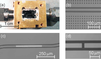
Onto these substrates we sputter-deposit a thick Nb film. The resonators are patterned into these films using optical lithography (OL) or electron beam lithography (EBL) and reactive ion etching. The CPW resonators are comprised of a wide center conductor separated from the ground plane by a wide gap on either side. The MS resonator has a conductor width of and a thick Nb layer on the backside of the substrate serving as ground. We compare samples with different substrate thicknesses and surface treatments to our standard process for Nb on a thick silicon substrate covered with SiO2 on both sides (cf. sample I in Tab. 1). For sample II and sample III, we use a substrate which is thick and we compare OL and EBL. As a surface treatment, we remove the SiO2 layer on top of the silicon substrate for sample IV using hydrofluric acid (HF). Sample V is fabricated on a thick sapphire substrate, which is in-situ cleaned by Ar ion beam etching before Nb sputter deposition. Sample VI has a gridded groundplane as shown in Fig. 1 (b). Sample VII and sample VIII are used to investigate the influence of Nb/Al interfaces in the center conductor of the resonator. For this purpose, we replace a long piece of the Nb center conductor by an Al strip of identical width and thickness as shown in Fig. 1 (c). The Al strip shares an long overlap with the Nb center conductor and is evaporated in an extra fabrication step. For sample VII, we additionally clean the Nb surface by means of in-situ Ar-ion milling before the Al evaporation to remove oxides and resist residues from the Nb surface. More details on the fabrication process are given in appendix A.
III Methods
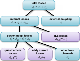
In this section we discuss the different contributions to microwave losses which we take into account in our analysis. An overview of these contributions is given in Fig. 2. In order to compare the internal losses of devices with different resonance frequencies , we calculate the internal quality factor as . Here, and are the loaded and the external quality factor, respectively. From VNA spectroscopy measurements we obtain the loaded quality factor , where is the full width at half maximum of the Lorentzian peak. We use a combination of microwave simulations and reference measurements to obtain for the CPW samples. This external quality factor applies for all resonators as they share the same layout for the coupling capacitor shown in Fig. 1 (d).
For our analysis, we calculate the losses , where is the well-known loss tangent. We split the internal losses into a power independent term and a power and temperature dependent TLS contribution . Hence, the internal losses are described as
| (1) |
Here, is the power circulating inside the resonator Sage et al. (2011) for the mode and is the power resonantly applied to the input of the resonator. In Eq. (1) describes losses due to the coupling of an ensemble of microscopic TLSs to the electromagnetic field of the resonator. These TLSs are located inside the dielectric and at the dielectric/metal interfaces in the vicinity of the resonator. For such a system, the TLS contribution reads Strom, von Schickfus, and Hunklinger (1978); Sage et al. (2011)
| (2) |
In this expression, the exponent is known to be design-dependent, Wang et al. (2009) is a characteristic power depending on the TLS properties, Schickfus and Hunklinger (1977); Arzeo, Lombardi, and Bauch (2014) and is the Boltzmann constant. Due to the distributed nature of the CPW resonator, TLS saturation does not occur uniformly across the sample but starts at voltage antinodes of the driven mode. Additionally, it depends on the center conductor width as well as on its separation to the groundplane , which determine the electric field strength. Gao et al. (2008b); Sage et al. (2011) In the low temperature and low power limit, the internal losses approach which is mainly limited by the unsaturated TLSs. The characteristic power is proportional to , where and represent the relaxation time of the TLSs and the broadening of the levels due to their mutual interaction, respectively. Schickfus and Hunklinger (1977) In the spin-boson model, the temperature dependence of follows a dependence Jäckle (1972); Leggett et al. (1987) which is proportional to for . Due to phonon mediated interaction between the TLSs one expects , where and describe the TLS coupling rate to acoustic and optical phonons, respectively. Rudin, Reinecke, and Segall (1990); Borri et al. (1999) For low temperatures, , the interaction is predominantly mediated by the term accounting for acoustic phonons . However, in the regime which is relevant for our experiments, a power law has been found for both, and . Jäckle (1972); Strom, von Schickfus, and Hunklinger (1978); Schickfus and Hunklinger (1977); Phillips (1987); Borri et al. (1999); Rudin, Reinecke, and Segall (1990); Lisenfeld et al. (2007, 2010) Therefore, the temperature dependence of the characteristic power can be approximated as Schickfus and Hunklinger (1977)
| (3) |
where is the absolute permittivity of the dielectric and is the effective dipole moment of the TLSs. For resonators made from a single metal layer, these TLSs couple mainly to the electric field generated by the CPW structure. This situation changes for resonators including metal/metal interfaces, e.g. Nb/Al interfaces, especially if these interfaces include an oxide layer of finite thickness . In this case, the interface forms a Josephson junction and the TLSs also couple to the electric field inside this junction. Martinis et al. (2005) Here, is the voltage drop across the junction induced by the resonator current . The Josephson inductance is given by , where is the electron charge, the junction critical current and the phase drop across the junction. Hence, the root mean square electric field across the junction reads as
| (4) |
Equation (4) shows that a finite resonator current amplitude leads to an electric field across the junction which couples to possible TLSs. Therefore, we can apply Eq. (2) to describe the losses generated by TLSs inside a Josephson junction which is formed by an oxidized metal/metal interface incorporated into the center conductor of a CPW resonator.
In the following, we focus on the high power regime where the internal losses are limited by
| (5) |
Here, are thermally induced quasiparticle losses and are eddy current losses on the backside of the substrate. The term comprises all other loss processes such as radiation, Kasilingam and Rutledge (1983) the finite surface resistance of superconductors, Noguchi, Naruse, and Sekimoto (2012) and nonthermal quasiparticles generated by stray infrared light. Barends et al. (2011); Gao et al. (2008a) Whereas dielectric losses dominate at very low temperatures, the losses related to the superconducting material typically become dominant when the sample temperature exceeds approximately of the critical temperature of the superconductor. Arzeo, Lombardi, and Bauch (2014) In the temperature range of our experiments, we expect a considerable quasiparticle contribution only for samples containing Al. Assuming that the superconducting material is in the dirty or local limit, the quasiparticle contribution can be described with the Matthis-Bardeen theory, Mattis and Bardeen (1958); Gao et al. (2008a)
| (6) |
Here, is the ratio of kinetic inductance to total inductance of the conductor, with the superconducting energy gap , , and are the modified Bessel function of the first and second kind, respectively.
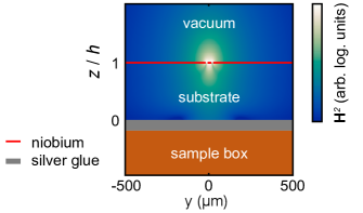
Eddy current losses in Eq. (5) mainly arise from the finite conductivity of the material used to fix our samples in the sample box. The thickness dependence results from a residual magnetic field on the backside of the substrate. Therefore, we also find a finite field in the volume of the silver glue used to fix our samples in the sample box (see Fig. 3). Inside the silver glue volume, the field decays exponentially in -direction for microwave frequencies within the skin depth , thus . The dissipated power due to eddy currents reads Morgan (1949) , where is the electrical conductivity at the resonator frequency and is the volume of the conductive material on the backside of the substrate. Even though would diverge for insulators, it is vaild for the conductive materials used in our work. To evaluate the thickness dependence, we calculate the field components of the magnetic field in the substrate following Ref. Simons and Arora, 1982. We modify this model by appropriate boundary conditions for the conductor-backed substrate demanding the -component of to vanish. The -component of , which points in the direction along the transmission line, can also be neglected in comparison with the -component. Using these assumptions, the field on the backside of the substrate can be written as . Assuming a sinusodial current distribution along the transmission line, we find , where is the resonator length and is the field distribution at along the -direction. The maximum field strength is given as . Here, and are line and vacuum impedance, respectively, and is the relative dielectric constant of the Si substrate. Finally, we calculate the dissipated power
| (7) |
In the above expression, , is the absolute permeability of the conductive material, Pel (2013) and we use . Maxwell (1947) The thickness dependent losses are defined as , the ratio of the power dissipated in the system to stored power. Hence,
| (8) |
which is independent of the power circulating inside the resonator.
IV Results
In the following, we present the experimental results starting with a comparison of TLS related losses. Next, we show how losses are affected by Nb/Al interfaces which are necessary for the galvanic coupling of Al-based Josephson circuits to the Nb center conductor of the CPW. Finally, we analyze the influence of a finite substrate thickness on internal losses.
IV.1 TLS losses in Nb resonators
In this subsection, we discuss the TLS losses for samples I – VI (pure Nb resonators). Fitting Eq. (1) to the power dependence of , we extract , and (see Fig. 4). The results are summarized in Table 1. To obtain further insight into the nature of the TLSs, we analyze the relative change , which is linked to TLS properties via Eq. (3). For each individual sample, we observe an increase in for increasing temperature due to the temperature dependent lifetime of the TLSs as shown in Fig. 5. From a fit based on Eq. (3), we find (average over samples I – VIII). This value deviates from expected from the spin-boson model, Jäckle (1972); Leggett et al. (1987) but is comparable to values reported for TLSs in glasses Phillips (1987); Schickfus and Hunklinger (1977) and phase qubits. Lisenfeld et al. (2007, 2010) The deviation can be attributed to the fact that our experiments are not in the low temperature limit, but rather in the intermediate regime .
Next, we discuss the low temperature and low power losses . For sample I, which serves as a reference sample, we find a TLS contribution . We now study the influence of TLSs near the surface using sample IV, where we have cleaned the surface with an HF-dip before metallization. For this sample, we measure , which is one order of magnitude lower than for sample I. Hence, we conclude that most of the TLS losses are introduced by the bulk SiO2 layer, the SiO2/metal, and SiO2/air surfaces. In contrast, losses at the metal/air interface are significantly smaller (). For sample VI (gridded groundplane) the TLS losses are comparable to those of a resonator with continuous groundplane.
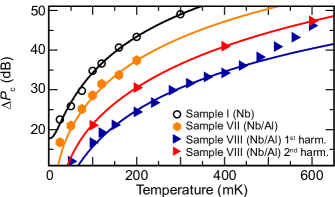
plotted versus temperature for different samples. Solid lines are fits of Eq. (3) to the data. For the first harmonic mode of sample VIII we observe a strong increase for temperatures above . For this dataset we fit only to datapoints below . For better visibility, there is an offset of between each dataset.
IV.2 Losses due to TLSs at Nb/Al interfaces
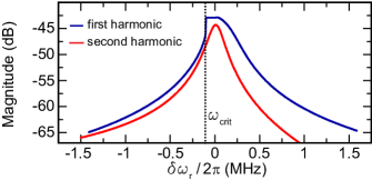
We use sample VIII, where an Al strip is placed at the current antinode of the fundamental mode, to study the influence of Nb/Al interfaces introduced into the center conductor of CPW resonators. These interfaces are known to introduce losses in galvanically coupled Josephson junction based circuits. Watanabe et al. (2009); Shcherbakova et al. (2015) However, the TLS effect on the internal quality factor of superconducting resonators has not yet been quantified. The transmission of the first harmonic mode of the resonator without ion gun treatment shows a deviation from the Lorentzian lineshape for large probe power (see Fig. 6). As this behavior is typical for resonators including Josephson junctions, Manucharyan et al. (2007); Watanabe et al. (2009) we treat the Nb/Al interfaces as large-area Josephson junctions. As expected, the second harmonic mode which has a current node at the interface position shows a Lorentzian behavior. Due to the presence of the interfaces, we also observe a non-equidistant mode spacing, which is again typical for resonators including Josephson junctions. Niemczyk et al. (2010) Specifically, we find , where is the resonance frequency of the mode. In contrast, all samples without Nb/Al interface (samples I–VI) show an equidistant mode spacing, .
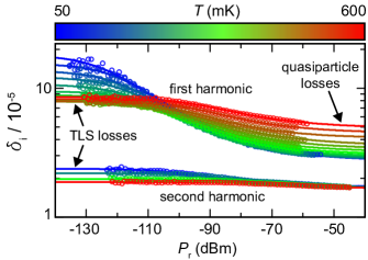
The presence of the oxidized interfaces results in large TLS losses. For the first harmonic mode of sample VIII, we observe an increase of more than one order of magnitude in compared to sample I (pure Nb) or sample VII (cleaned Nb/Al interface). Hence, we draw two important conclusions. First, without cleaning step, the Nb oxides present at the interfaces are strong TLS sources. Second, these TLSs can cause significant losses. This behavior is not immediately obvious, because the Nb/Al interfaces are placed at a voltage node of the first harmonic mode. Consequently, the TLSs associated with the Nb oxides at these interfaces are not expected to couple to the resonator electric field. Nevertheless, due to the electric field between the Nb and the Al layer in the overlap area, we observe a pronounced power and temperature dependence of (see Fig. 7). Actually, according to Eq. (4), is proportional to the resonator current and therefore maximum if the Nb/Al interface is placed at the current antinode (voltage node) of the resonator field.
In the following, we discuss why the TLSs in the interfaces are not yet saturated by for a probe power corresponding to the vacuum current , which is necessary to observe the power dependence shown in Fig. 7. From the critical points as indicated in Fig. 6, we can derive the critical current Manucharyan et al. (2007) , where is the resonator inductance. With a junction area of approximately , we obtain a current density . This very low critical current density is expected, as the Nb was exposed to air for two days. Kleinsasser, Miller, and Mallison (1995) Nevertheless, we obtain and can use the approximation . Assuming an oxide thickness on the order of , we obtain from Eq. (4). On the one hand, this field is large enough to mediate a coupling between the TLSs and the resonator. On the other hand, it is small compared to the experimentally observed saturation field given by the resonator current for m.
In the next step, we confirm our model of TLS losses in the interfaces by analyzing the second harmonic mode of sample VIII, which has a voltage antinode at the interface position. As shown in Fig. 7, this mode shows significantly less internal losses than the first harmonic mode. We measure and , that is, values comparable to those of the first harmonic mode of the pure Nb resonator (sample I). This observation is unexpected for losses based on a model considering only uniformly distributed loss mechanisms. Göppl et al. (2008) Instead, the effect can be explained by TLSs localized in the Nb/Al interfaces. Since for the second harmonic mode the interfaces are placed at the current node, , the corresponding electric field is vanishingly small. Therefore, only the TLSs outside the interface, which couple to the resonator electric field, introduce losses comparable to those of sample I (pure Nb). We note that also the power independent contribution is smaller for the second harmonic mode than for the first harmonic mode. This behavior indicates that the interfaces are not only strong sources for TLS losses but also for local resistive losses.
Finally, we show that the local losses induced by the interfaces can be significantly reduced by in-situ ion gun treatment of the Nb surface before Al evaporation. Consequently, of the fundamental mode of sample VII (ion gun treatment) is one order of magnitude larger than for sample VIII (no ion gun treatment). As expected, we find that of sample VII is similar to of both the second harmonic mode of sample VIII and the fundamental mode of sample I (pure Nb).
IV.3 Temperature dependent losses in Nb/Al interfaces
We first analyze the temperature dependence for both samples including a Nb/Al interface (sample VII and sample VIII). As shown in Fig. 5, the exponent is in the same range as for all other samples (see Sec. IV.1). Specifically, we extract (sample VII), (sample VIII, first harmonic), and (sample VIII, second harmonic). When extracting for the first harmonic of sample VIII, we only take datapoints below into acount. We attribute the increased slope of above this temperature to self heating processes Lang et al. (2003); Tholen et al. (2007); Wang et al. (2005); Guénon et al. (2010) inside the interfaces. This effect is not present in the second harmonic of sample VIII which has a current node at the interface position.
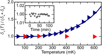
Next, we study the influence of the Nb/Al interfaces on , i.e., in the high power regime. For pure Nb resonators, we observe no significant change of in the temperature range between and . This behavior is expected because the number of quasiparticles is negligible for our experiments due to the critical temperature of the Nb films. However, the situation is different for samples including an Al strip, which has a lower . In Fig. 8, we show the temperature dependence of for the first two modes of sample VIII. For the first harmonic mode, we observe a quasiparticle induced increase of , which becomes relevant for temperatures above . Using obtained from a power sweep at where quasiparticles are negligible, we fit Eq. (5) to the data and find a kinetic inductance fraction of . This value is two orders of magnitude smaller than values reported in literature. Gao et al. (2008a) We explain this difference by the fact that the length of the Al strip is only of the total length of the center conductor. In contrast to the first harmonic mode, of the second harmonic mode shows no temperature dependence because the current distribution of the resonator has a node at the Al position in this case. Hence, quasiparticles in the Al do not carry a significant amount of the current circulating inside the resonator. Therefore, we conclude that also with respect to quasiparticle losses it is advantageous to place such interfaces at current nodes.
Due to the reduced superconducting energy gap of Al compared to Nb, nonequilibrium quasiparticles generated by stray infrared light can be trapped in the Al layer, Booth et al. (1993); Court et al. (2008) which reduces the number of quasiparticles in the Nb part of the center conductor. This effect can be used to decrease quasiparticle losses for resonator modes that have a current node at the Al layer. Indeed, we measure for the second harmonic mode of both samples including Al layers, which is smaller than measured for the second harmonic mode of sample I (pure Nb resonator).
Due to variations in the experimental environment, loss rates can vary as a function of time at a minutes timescale. Burnett et al. (2014); Müller et al. (2015) In the inset of Fig. 8 we show the fluctuations of over a minute time interval. From the statistics we evaluate a relatively small standard deviation . Also over a period of several days we do not observe any significant change in the resonator losses.
IV.4 Eddy current losses
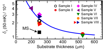
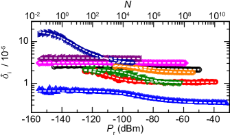
In this subsection we analyze losses resulting from eddy currents which are induced in the conductive material on the backside of the substrate. For this analysis, we compare all CPW samples fabricated by optical lithography. We observe that shows a significant dependence on the substrate thickness as displayed in Fig. 9. Assuming a negligible quasiparticle contribution , a numerical fit based on Eq. (5) and Eq. (8) yields and . This conductivity is approximately hundred times larger than the room temperature conductivity of our silver glue Pel (2013) and comparable to the room temperature conductivity of copper. Maxwell (1947); Thorp (1954) Since our experiments are carried out at low temperatures where the conductivity of metals typically increases by a factor of , Matula (1979); Fouaidy and Hammoudi (2006) we can quantitatively explain the loss behavior shown in Fig. 9 by ohmic losses in the silver glue. The influence of eddy current losses depends on the material present underneath the sample. Compared to pure metals, silver glue has a relatively low conductivity and therefore larger losses. For samples with a substrate thickness of losses are already enhanced by compared to in the high power regime. Samples fabricated on thick substrates show a loss increase by a factor of four compared to . The slight scatter in for is attributed to our assumption of a universal . This assumption is, of course, only a rough estimation because the samples are fabricated with different cleaning methods.
In summary, we can quantitatively explain losses due to eddy currents using numerical calculations of the -field distribution in conductor backed CPW structures. The electrodynamical model suggests that it is advantageous to either use thick substrates or materials with high conductivity on the backside of the substrate. Therefore, losses caused by eddy currents can be avoided by using superconducting materials at this position. This conclusion is supported by our measurements on the MS resonator (sample IX), which is fabriacated on a thick substrate and employs a superconducting ground plane. For this sample, we measure , which is reduced compared to the values of the other samples fabricated on a thick substrate by a factor of two, despite the fact that the field at the bottom surface of the substrate is an order of magnitude larger compared to the CPW samples.
In contrast to other groups, Quintana et al. (2014) we observe a decrease of the power independent losses by a factor of three for the sample fabricated with EBL (sample III) compared to sample II, which is fabricated with OL. There are two likely reasons for this observation. First, the Nb edges are smoother for the EBL sample than for the OL samples, resulting in a reduced field elevation at these positions. Second, compared to our OL process, the PMMA resist used for EBL may leave less resist residuals on the sample. Such resist residuals are known to introduce losses. Quintana et al. (2014)
V Conclusions
We fabricate superconducting CPW resonators and analyze mechanisms leading to microwave losses. With respect to TLS losses, we find that the characteristic power necessary to saturate TLSs shows a pronounced temperature dependence. Specifically, we extract an exponent for the polynomial part of this temperature dependence. Furthermore, we show that an HF-dip can be used to remove TLSs and therefore reduce losses on oxide covered silicon substrates. In addition, we investigate resonators containing Nb/Al interfaces, which typically occur for galvanically coupled quantum circuits. We quantitatively investigate the temperature and power dependence of the losses caused by these interfaces. These losses can be reduced by either placing the interfaces in a current node or by removing the oxide layer containing the TLSs by in-situ Ar ion milling. In the high power limit, where the TLSs are saturated, we observe temperature dependent losses induced by quasiparticle excitations in the Al. Finally, we investigate losses generated by eddy currents in the conductive material on the backside of the substrate. Our results show that the usage of thick enough substrates or metals with high conductivity on the substrate backside helps to minimize these losses.
This work is supported by the German Research Foundation through SFB 631 and FE 1564/1-1, EU projects CCQED, PROMISCE, the doctorate program ExQM of the Elite Network of Bavaria.
References
- Schoelkopf and Girvin (2008) R. J. Schoelkopf and S. M. Girvin, Nature 451, 664 (2008).
- Niemczyk et al. (2010) T. Niemczyk, F. Deppe, H. Hübl, E. P. Menzel, F. Hocke, M. J. Schwarz, J. J. Garcia-Ripoll, D. Zueco, T. Hümmer, E. Solano, A. Marx, and R. Gross, Nat. Phys. 6, 772 (2010).
- Kubo et al. (2011) Y. Kubo, C. Grezes, A. Dewes, T. Umeda, J. Isoya, H. Sumiya, N. Morishita, H. Abe, S. Onoda, T. Ohshima, V. Jacques, A. Dréau, J.-F. Roch, I. Diniz, A. Auffeves, D. Vion, D. Esteve, and P. Bertet, Phys. Rev. Lett. 107, 220501 (2011).
- Mariantoni et al. (2011) M. Mariantoni, H. Wang, R. C. Bialczak, M. Lenander, E. Lucero, M. Neeley, A. D. O ’Connell, D. Sank, M. Weides, J. Wenner, T. Yamamoto, Y. Yin, J. Zhao, J. M. Martinis, and A. N. Cleland, Nat. Phys. 7, 287 (2011).
- Hofheinz et al. (2009) M. Hofheinz, H. Wang, M. Ansmann, R. C. Bialczak, E. Lucero, M. Neeley, A. D. O’Connell, D. Sank, J. Wenner, J. M. Martinis, and A. N. Cleland, Nature 459, 546 (2009).
- Wisbey et al. (2010) D. S. Wisbey, J. Gao, M. R. Vissers, F. C. S. da Silva, J. S. Kline, L. Vale, and D. P. Pappas, J. Appl. Phys. 108, 093918 (2010).
- Wenner et al. (2011a) J. Wenner, R. Barends, R. C. Bialczak, Y. Chen, J. Kelly, E. Lucero, M. Mariantoni, A. Megrant, P. J. J. O’ Malley, D. Sank, A. Vainsencher, H. Wang, T. C. White, Y. Yin, J. Zhao, A. N. Cleland, and J. M. Martinis, Appl. Phys. Lett. 99, 113513 (2011a).
- Sage et al. (2011) J. M. Sage, V. Bolkhovsky, W. D. Oliver, B. Turek, and P. B. Welander, J. Appl. Phys. 109, 063915 (2011).
- Ohya et al. (2014) S. Ohya, B. Chiaro, A. Megrant, C. Neill, R. Barends, Y. Chen, J. Kelly, D. Low, J. Mutus, P. J. J. O’Malley, P. Roushan, D. Sank, A. Vainsencher, J. Wenner, T. C. White, Y. Yin, B. D. Schultz, C. J. Palmstrom, B. A. Mazin, A. N. Cleland, and J. M. Martinis, Supercond. Sci. Tech. 27, 015009 (2014).
- O’ Connell et al. (2008) A. D. O’ Connell, M. Ansmann, R. C. Bialczak, M. Hofheinz, N. Katz, E. Lucero, C. McKenney, M. Neeley, H. Wang, E. M. Weig, A. N. Cleland, and J. M. Martinis, Appl. Phys. Lett. 92, 112903 (2008).
- Arzeo, Lombardi, and Bauch (2014) M. Arzeo, F. Lombardi, and T. Bauch, Appl. Phys. Lett. 104, 212601 (2014).
- Barends et al. (2011) R. Barends, J. Wenner, M. Lenander, Y. Chen, R. C. Bialczak, J. Kelly, E. Lucero, P. O’ Malley, M. Mariantoni, D. Sank, H. Wang, T. C. White, Y. Yin, J. Zhao, A. N. Cleland, J. M. Martinis, and J. J. A. Baselmans, Appl. Phys. Lett. 99, 113507 (2011).
- Gao et al. (2008a) J. Gao, J. Zmuidzinas, A. Vayonakis, P. Day, B. Mazin, and H. Leduc, J. Low Temp. Phys. 151, 557 (2008a).
- Lindström et al. (2009) T. Lindström, J. E. Healey, M. S. Colclough, C. M. Muirhead, and A. Y. Tzalenchuk, Phys. Rev. B 80, 132501 (2009).
- Khalil et al. (2012) M. S. Khalil, M. J. A. Stoutimore, F. C. Wellstood, and K. D. Osborn, J. Appl. Phys. 111, 054510 (2012).
- Fano (1961) U. Fano, Phys. Rev. Lett. 124, 1866 (1961).
- Megrant et al. (2012) A. Megrant, C. Neill, R. Barends, B. Chiaro, Y. Chen, L. Feigl, J. Kelly, E. Lucero, M. Mariantoni, P. OMalley, D. Sank, A. Vainsencher, J. Wenner, T. White, Y. Yin, J. Zhao, C. Palmström, J. M. Martinis, and A. Cleland, Appl. Phys. Lett. 100, 113510 (2012).
- Wenner et al. (2011b) J. Wenner, M. Neeley, R. C. Bialczak, M. Lenander, E. Lucero, A. D. O’Connell, D. Sank, H. Wang, M. Weides, A. N. Cleland, and J. M. Martinis, Supercond. Sci. Tech. 24, 065001 (2011b).
- Hornibrook, Mitchell, and Reilly (2012) J. M. Hornibrook, E. E. Mitchell, and D. J. Reilly, (2012), arXiv:1203.4442 [cond-mat] .
- Baust et al. (2015) A. Baust, E. Hoffmann, M. Haeberlein, M. J. Schwarz, P. Eder, J. Goetz, F. Wulschner, E. Xie, L. Zhong, F. Quijandría, B. Peropadre, D. Zueco, J.-J. García Ripoll, E. Solano, K. Fedorov, E. P. Menzel, F. Deppe, A. Marx, and R. Gross, Phys. Rev. B 91, 014515 (2015).
- Shcherbakova et al. (2015) A. V. Shcherbakova, K. G. Fedorov, K. V. Shulga, V. V. Ryazanov, V. V. Bolginov, V. A. Oboznov, S. V. Egorov, V. O. Shkolnikov, M. J. Wolf, D. Beckmann, and A. V. Ustinov, Supercond. Sci. Tech. 28, 025009 (2015).
- Watanabe et al. (2009) M. Watanabe, K. Inomata, T. Yamamoto, and J.-S. Tsai, Phys. Rev. B 80, 174502 (2009).
- Leggett et al. (1987) A. J. Leggett, S. Chakravarty, A. T. Dorsey, M. P. A. Fisher, A. Garg, and W. Zwerger, Rev. Mod. Phys. 59, 1 (1987).
- Phillips (1987) W. A. Phillips, Rep. Progr. Phys. 50, 1657 (1987).
- Nsanzineza and Plourde (2014) I. Nsanzineza and B. L. T. Plourde, Phys. Rev. Lett. 113, 117002 (2014).
- Niemczyk et al. (2009) T. Niemczyk, F. Deppe, M. Mariantoni, E. P. Menzel, E. Hoffmann, G. Wild, L. Eggenstein, A. Marx, and R. Gross, Supercond. Sci. Tech. 22, 034009 (2009).
- Strom, von Schickfus, and Hunklinger (1978) U. Strom, M. von Schickfus, and S. Hunklinger, Phys. Rev. Lett. 41, 910 (1978).
- Wang et al. (2009) H. Wang, M. Hofheinz, J. Wenner, M. Ansmann, R. C. Bialczak, M. Lenander, E. Lucero, M. Neeley, A. D. O’Connell, D. Sank, M. Weides, A. N. Cleland, and J. M. Martinis, Appl. Phys. Lett. 95, 233508 (2009).
- Schickfus and Hunklinger (1977) M. V. Schickfus and S. Hunklinger, Phys. Lett. A 64, 144 (1977).
- Gao et al. (2008b) J. Gao, M. Daal, J. M. Martinis, A. Vayonakis, J. Zmuidzinas, B. Sadoulet, B. A. Mazin, P. K. Day, and H. G. Leduc, Applied Physics Letters 92, 212504 (2008b), dx.doi.org/10.1063/1.2937855.
- Jäckle (1972) J. Jäckle, Z. Phys. 257, 212 (1972).
- Rudin, Reinecke, and Segall (1990) S. Rudin, T. L. Reinecke, and B. Segall, Phys. Rev. B 42, 11218 (1990).
- Borri et al. (1999) P. Borri, W. Langbein, J. M. Hvam, and F. Martelli, Phys. Rev. B 59, 2215 (1999).
- Lisenfeld et al. (2007) J. Lisenfeld, A. Lukashenko, M. Ansmann, J. M. Martinis, and A. V. Ustinov, Phys. Rev. Lett. 99, 170504 (2007).
- Lisenfeld et al. (2010) J. Lisenfeld, C. Müller, J. H. Cole, P. Bushev, A. Lukashenko, A. Shnirman, and A. V. Ustinov, Phys. Rev. Lett. 105, 230504 (2010).
- Martinis et al. (2005) J. M. Martinis, K. B. Cooper, R. McDermott, M. Steffen, M. Ansmann, K. D. Osborn, K. Cicak, S. Oh, D. P. Pappas, R. W. Simmonds, and C. C. Yu, Phys. Rev. Lett. 95, 210503 (2005).
- Kasilingam and Rutledge (1983) D. Kasilingam and D. Rutledge, in Microwave Symposium Digest, IEEE MTT-S International (1983) pp. 113–116.
- Noguchi, Naruse, and Sekimoto (2012) T. Noguchi, M. Naruse, and Y. Sekimoto, Phys. Procedia 36, 318 (2012).
- Mattis and Bardeen (1958) D. C. Mattis and J. Bardeen, Phys. Rev. 111, 412 (1958).
- Morgan (1949) S. P. Morgan, J. Appl. Phys. 20, 352 (1949).
- Simons and Arora (1982) R. Simons and R. Arora, IEEE T. Microw. Theory 30, 1094 (1982).
- Pel (2013) “Product no. 16062 - pelco conductive silver paint,” Tech. Rep. (TED PELLA. INC., 2013).
- Maxwell (1947) E. Maxwell, J. Appl. Phys. 18, 629 (1947).
- Manucharyan et al. (2007) V. E. Manucharyan, E. Boaknin, M. Metcalfe, R. Vijay, I. Siddiqi, and M. Devoret, Phys. Rev. B 76, 014524 (2007).
- Kleinsasser, Miller, and Mallison (1995) A. Kleinsasser, R. Miller, and W. Mallison, IEEE T. Appl. Supercon. 5, 26 (1995).
- Göppl et al. (2008) M. Göppl, A. Fragner, M. Baur, R. Bianchetti, S. Filipp, J. M. Fink, P. J. Leek, G. Puebla, L. Steffen, and A. Wallraff, J. Appl. Phys. 104, 113904 (2008).
- Lang et al. (2003) K. Lang, S. Nam, J. Aumentado, C. Urbina, and J. M. Martinis, IEEE T. Appl. Supercon. 13, 989 (2003).
- Tholen et al. (2007) E. A. Tholen, A. Ergül, E. M. Doherty, F. M. Weber, F. Gregis, and D. B. Haviland, Appl. Phys. Let. 90, 253509 (2007).
- Wang et al. (2005) H. B. Wang, T. Hatano, T. Yamashita, P. H. Wu, and P. Müller, Appl. Phys. Lett. 86, 023504 (2005).
- Guénon et al. (2010) S. Guénon, M. Grünzweig, B. Gross, J. Yuan, Z. G. Jiang, Y. Y. Zhong, M. Y. Li, A. Iishi, P. H. Wu, T. Hatano, R. G. Mints, E. Goldobin, D. Koelle, H. B. Wang, and R. Kleiner, Phys. Rev. B 82, 214506 (2010).
- Booth et al. (1993) N. Booth, P. Brink, R. Gaitskell, D. Goldie, A. Hahn, G. Salmon, and A. Swift, Journal of Low Temperature Physics 93, 521 (1993).
- Court et al. (2008) N. A. Court, A. J. Ferguson, R. Lutchyn, and R. G. Clark, Phys. Rev. B 77, 100501 (2008).
- Burnett et al. (2014) J. Burnett, L. Faoro, I. Wisby, V. L. Gurtovoi, A. V. Chernykh, G. M. Mikhailov, V. A. Tulin, R. Shaikhaidarov, V. Antonov, P. J. Meeson, A. Y. Tzalenchuk, and T. Lindström, Nat Commun 5, (2014).
- Müller et al. (2015) C. Müller, J. Lisenfeld, A. Shnirman, and S. Poletto, Phys. Rev. B 92, 035442 (2015).
- Thorp (1954) J. Thorp, Proc. of the IEEI - Part III: Radio and Communication Engineering 101, 357 (1954).
- Matula (1979) R. A. Matula, J. Phys. Chem. Ref. Data 8, 1147 (1979).
- Fouaidy and Hammoudi (2006) M. Fouaidy and N. Hammoudi, Physica C 441, 137 (2006).
- Quintana et al. (2014) C. M. Quintana, A. Megrant, Z. Chen, A. Dunsworth, B. Chiaro, R. Barends, B. Campbell, Y. Chen, I.-C. Hoi, E. Jeffrey, J. Kelly, J. Y. Mutus, P. J. J. O’Malley, C. Neill, P. Roushan, D. Sank, A. Vainsencher, J. Wenner, T. C. White, A. N. Cleland, and J. M. Martinis, Appl. Phys. Lett. 105, 062601 (2014).
Appendix A Sample fabrication
Here, we give a detailed description of our fabrication processes. All substrates have lateral dimensions of and are cleaned by a series of isopropanol and acetone dips in an ultrasonic bath. We sputter deposit the thick niobium films with a deposition rate of at an argon pressure of with an argon flow of sccm.
For optical lithography we use AZ5214E resist, which is spin-coated onto the Nb with rpm. We perform mask exposure to ultraviolet light after baking for at . For electron beam lithography we use PMMA/MA 33 % resist spin-coated with 2000 rpm for one minute. To activate the resist, we use a dose of and develop with AR 600-56 developer.
For reactive ion etching we use an Ar/SF6 plasma with a flow of 10 sccm for Ar and 20 sccm for SF6. We etch for at a pressure of using for the ICP plasma.
For sample IV, we remove the SiO2 layer on top of the Si substrate. To this end, we wet-etch for three minutes with a ratio HF:H2O = 1:10. Afterwards, we rinse the sample with deionized water before placing it in the sputtering chamber within five minutes after the wet etch. Sample V is additionally cleaned by in-situ Ar ion milling for before sputter deposition. Here, we use an acceleration voltage of , an operating pressure of , a filament current of , and an emission current of . The square holes of sample VI have a width of and are separated by . Aluminum evaporation for sample VII and sample VIII is done at with and a filament current of , which results in a rate of . To clean the Nb surface of sample VII, we use an Ar ion milling process for with an Ar flow of sccm, an emission current of , an extraction voltage of , and an acceleration voltage of .