Cascade donor-acceptor organic ferroelectric layers, between graphene sheets, for solar cell applications.
Abstract
Organic ferroelectric layers sandwiched between the graphene sheets are presented as a model of the solar cell. The investigated systems display many advantageous properties: 1) the cascade energy-levels alignment, 2) simultaneous donor and acceptor character depending on the charge-carrier direction, 3) the charge-transfer excitonic type, 4) the induced polarization of the electrodes, leading to a substantial work-function change of the anode and cathode - around 1.5 eV, respectively.
I Introduction
The power consumption and environmental pollution triggers scientists for an intensive search of the efficient photovoltaic materials. One of the key factors of the solar-cell efficiency is the supressed recombination of the charge carriers. This supression can be achieved via introduction of the charge trapping layers trap , and/or by the manipulation of the energy-level alignment cascade . Designing the heterostructure, that exhibits the cascade energy levels for the holes and electrons is tricky. On the other hand, if one applies the multilayers of the same material - which, in addition, is ferroelectric - then the Stark effect shifts the energy levels of the subsequent layers gradually. Recently published theoretical studies by Sobolewski Sobol , of the ferroelectric columnar clusters in the context of the organic photovoltaics without p-n junctions, concern molecules with the dipole moment. The molecular orbitals of the subsequent energy levels, in that work, are well localized at the corresponding molecular rings in the stack; especially for the top and bottom molecules.
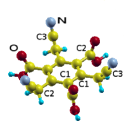
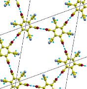
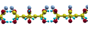
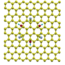
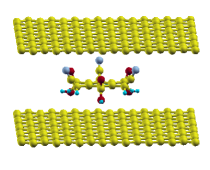
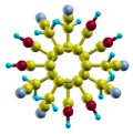
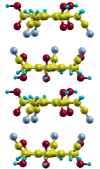
Our systems are composed of the flat molecules, named 1,3,5-tricyano-2,4,6-tricarboxy-benzene. The formula might be written as C6-3(NCCH2)-3(OCOH). These molecules consist of the central aromatic ring. Every second carbon of the ring is terminated with the cyano group possessing the dipole moment - standing out of the ring planes - and alternated with the carboxy groups, which form the intermolecular hydrogen bonds within the planes. This is for the purpose of the minimization of the electronic transport within the planes. The molecule with indexed atoms, as well as the top and side views on the single molecular layer are presented in Fig. 1. These networks can be stacked one on top of the other in various ways, but for the electronic transport the AA-type is favored. Considered structure resemble the 2D covalent metal-organic frameworks Bein-1 ; Bein-2 , however the intermolecular hydrogen bonds are used here instead of the covalent bonds. These molecular layers are sandwiched between the graphene sheets that act as the electrodes. The interlayer transport across our stacks is of the - type, and it strongly depends on the overlap between the orbitals of carbons within the molecular central part and those of the neighboring molecule, as well as the distance between the top atoms of the dipole group and the bottom hydrogens of the next top molecule.
Each ferrolectric monolayer in the stack acts as a donor of the electrons to the next deeper-laying layer, and simultaneously as an acceptor of the electrons from neighboring above-laying layer. According to our knowledge, this is the first system - except the columns in the work Sobol - where donor and acceptor (D-A) functionality is combined within the same molecule. Therefore, these layers will operate in a very similar way to the integrated heterojunctions Bein-2 or bulk heterojunctions BHJ ; IBHJ , where two materials of different D-A functionality interpenetrate each other in the ”bulk” of the optically active region.
Interestingly, the proximity of the molecular dipole moment polarizes the top and bottom electrode in opposite directions. The induced change of the surface dipole moment influences the work function, in such a way that it is higher for the anode and lower for the cathode. This is the advantageous feature. Similar properties are exhibited by graphene with the deposited ferroelectric layer - recent patent patent1 ; patent2 , with the documented efficiency of the photovoltaic effect about 2. The same idea of the addition of the ferroelectric elements has been applied in the 1D quantum-dot solar cells decorated with the molecules possessing the dipole moment QCdipole .
II Computational details
The density-functional theory calculations were performed using the Quantum ESPRESSO suite of codes (QE) qe . This package is based on the plane-wave basis set and the pseudopotentials for the core electrons. The exchange-correlation functional was chosen for the gradient corrected Perdew-Burk-Erzenhof parametrization PBE . The ultrasoft pseudopotentials USPP were used with the energy cutoffs 30 Ry and 300 Ry for the plane-waves and the density, respectively. It has been checked that increasing these values to 40 and 400 Ry, respectively, changes the band energies by less than 0.002 eV and relative conformation energies of the ferroelectric and antiferroelectric molecular wire by less than 0.001 eV. The Monkhorst-Pack uniform k-mesh in the Brillouin zone has been set to for the slab with two molecules per the elementary cell, and for the wire with one molecule per cell (for two molecules per cell, the corresponding k-mesh was ), which was enough due to large supercells. The vacuum separation between the periodic slabs was around 40 Å.
In order to obtain the band structures projected onto the local groups of atoms, we employed the wannier90 package w90 , which interpolates bands using the maximally-localized Wannier functions wan ; RMP . The same tool has been used for the calculations of the dipole moment and polarization. For the Wannier optimization procedure, we used the k-point mesh of the same accuracy as for the self-consistent DFT calculations. The number of Wannier functions was the same as the number of electrons in the system. The outer and inner windows were chosen in such a way, that they were identical and their border energies were placed within the energy gaps between the groups of the composite bands. For metallic systems, such as molecule between the graphene sheets, the calculation of the Wannier occupation numbers was necessary. We used the k-point dependent procedure, being an extension of that used in the van der Waals functionals VdW , and previously tested by us for GaAs doped with Mn gamnas .
The dipole moment can be easily obtained from the maximally-localized-Wannier centers positions, , using the formula
| (1) |
where and are the atomic pseudopotential charge and its position, and indexes and run over the number of atoms and Wannier functions, respectively. The above simple Wannier approach is based on the modern theory of polarization polar - which was previously used in the calculations of other photovoltaic 2D system giova .
III Results
The geometries of the investigated systems have been optimized, and the intermolecular distance in the AA-type stack is 5.2 Å. The distance between the top molecule and the top graphene is the same as that between the molecules, and on the bottom it is smaller, of order 4.6 Å. The lateral intermolecular distance between the molecules can be described by the OH…O bond, which is 1.75 Å.
III.1 Dipole moment.
Systems presented in Fig. 1 are built of molecules containing two types of groups with the dipole moment: 1) OCOH and 2) NCCH2. The first group is in the plane perpendicular to the plane of the central carbon ring. The dipole moment of this group is oriented from O to OH. Due to the fact, that this group plays the role of chemical connection between the molecules, some molecules have the OH part above the carbon-ring plane and the neighboring molecules have this group below the central part plane. Therefore, in total there is no dipole moment originating from the intermolecular bonds within the layer, as it is in other hydrogen-bonded molecular systems Horiuchi-1 ; Horiuchi-2 . In contrast, the second group plays the role of the polarization source, with the dipole moment oriented from N down to the central C-ring plane.
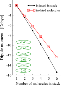
The calculated dipole moment of an isolated molecule is -2.06 Debye. When the molecules are placed in the column, then the proximity of other dipoles induce larger polarization. The induced dipole moment in the column of molecules is presented in Fig. 2. The molecules placed in the middle of the finite number stack are characterized by the larger induced polarization - about 10 - than the molecules at the top and bottom of the column.
We emphasize, the total dipole moment from the multilayer – i.e. the monolayers which are in the middle of the stack – does not cancel as in the bulk ferroelectrics. This is because the interactions between the layers are of the van der Waals type, and molecules do not form the chemical bonds between the layers. Thus, the electronic polarization at the molecular dipoles feels the neighboring layer very weakly.
III.2 Cascade energy-levels alignment and combined donor-acceptor functionality.
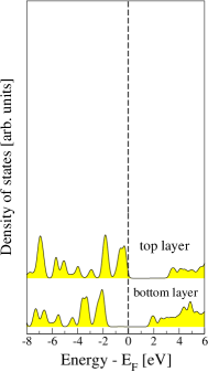
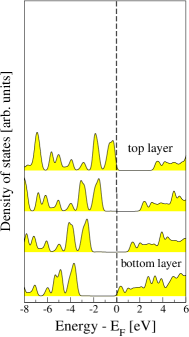
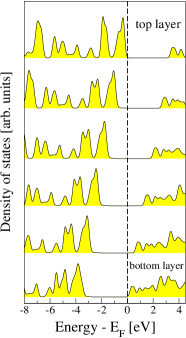
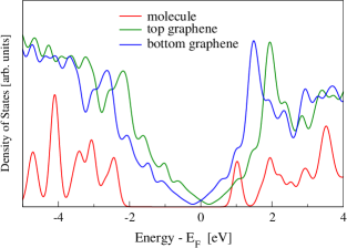
The energy gap in the band structure of a single molecular layer is about 3.66 eV. For the 6-layer thick slab, the single-layer energy gap decreases to around 3.4 eV. While the total energy gap of the system closes due to the Stark effect, which shifts the top and bottom layer towards higher and lower energies, respectively. The intermediate layers shift gradually in the energy, forming a cascade of red the hole- and electron-energy levels, when moving step by step from the top to the bottom electrode. In Fig. 3, the density of states (DOS) projected onto each layer separately is presented, for the 2-, 4- and 6-layer stack. The overal energy gap for the 2-layer case is half of that for the single layer. In the case of 4-layer stack, the total band gap closes. Increase of the number of molecular layers lowers the step of the energy shift of the neighboring layers. The shape of the projected DOS is only slightly changed between the layers and as a function of their number. In our case, the cascade energy-level alignment is obtained, practically without need of band engineering; which is the usual case when many materials are used in the heterojunctions cascade . Such cascade is a very desired property in order to avoid the recombination of the charge carriers.
Donor or acceptor character of each layer depends on its position with respect to the next layer - whether the carriers arrive from the anode or cathode - although all layers have identical atomic structure. Due to our knowledge, this is the first material which shows the property of donor- and acceptor-type mimetism within the same layer. It is advantageous, because one can obtain the functionality of the sophisticated bulk heterojunctions BHJ by using only one 2D material stacked in multilayers.
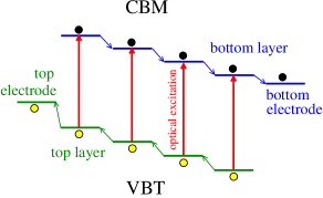
Fig. 4 schematically shows the operation of the cascade energy-level system with the electrodes, whose bands energetics follow the sequence of the electron and hole energy levels of the optically active material. Each single optical excitation creates one hole-electron pair at one layer. Then, the holes move towards higher energies within a manifold of the valence band states and the electrons move down within the conduction band levels. This way, the charge carrier transport across the optically active layers towards the electrodes takes place. Its efficiency is additionally factorized by the excitonic character and the work function of the molecular layers and the electrodes.
III.3 Exciton localization.
Excitons - the electron-hole pairs - can be described as the difference of the charge distribution before and after the absorption of light. If this difference is spacially localized, we have so-called Frenkel excitons. The extended excitations are of the Wannier-Mott type. The excitons move through the system as a pair before splitting - which might end with the delayed fluorescence and recombination instead of wanted charge separation. Moreover, in the molecular or very small quantum dot systems, the excitations lead to the singlet state, with the short life-time, or - after irradiative transitions - to the longer lived triplet state. The excitonic localization character is one of the indicators of the photovoltaic efficiency.
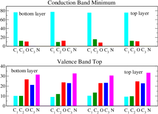
Therefore, we analize the atomic composition of the DOS at the hole and electron peaks in the VBT and CBM, respectively. In Fig. 5, we denote the central-ring carbons as C1, the adjacent carbons as C2, and the farther carbons connected to N as C3. The DOS projected at these groups of carbons, as well as nitrogens and oxygens, is pictured for the peak maximum at the VBT and CBM; separately for each molecular plane of the 4-layer system. The values are normalized to the total DOS and given in percentage. It is important to note that the lowest excited electronic states are composed mainly of carbons in the central ring. The hole states are delocalized over the dipole groups. The component from the central part of the molecule to the hole states is only 10. The above observations are true for all layers in the stack. As follows, our electron-hole pairs result from the excitation of the valence electrons localized around the the anion (groups containing N) into empty states localized around cation (the central benzene ring). Such pairs are called the charge-transfer excitons. A quick estimation for the Bohr exciton radius in our systems is about 4.7 Å. It is defined as the distance between the center of the molecule and one of the nitrogen atoms. Therefore, we have Frenkel-type charge-transfer excitonic material. Interestingly, the charge-transfer excitons are also formed at van der Waals interfaces of other materials CT-vdW .
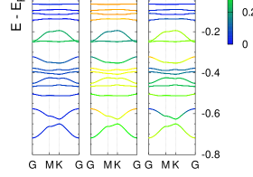
For further insight into a localization of electrons and holes, we project the band structures onto those maximally-localized Wannier functions which are centred near chosen groups of atoms. These plots are presented in Fig. 6 for carbons of the central ring, nitrogens and oxygens. The figure confirms our previous result, that the central-ring atoms are involved in the conduction states and the dipole and oxygen groups in the valence states. Moreover, we can see that using the OH…O bonds prohibits the electronic and hole transport within the molecular planes; which is obvious from the flat band structures.
III.4 Work function change caused by proximity of ferroelectric layers.
The dipole moment of molecules induces the charge polarization within the graphene layers. In order to estimate the strength of this polarization, we performed the calculations for the periodic system with large elementary cell, which contains a single molecule between the graphene layers on top and bottom. The number of carbon atoms in each graphene part in that cell is 160. The top and side views on this elementary cell are presented in Fig. 7. The figure contains also the plot of the DOS projected onto the molecule and the graphene sheets. The DOS shift of the top and bottom graphene layers, by about 0.2 eV for each electrode, is caused by the Stark effect and leads to the small charge transfer between the leads.
Using the Wannier-functions technique, described in the ”computational details”, we estimated the induced dipole moment in the top graphene as -2.58 Debye and the bottom graphene as +2.54 Debye; within the elementary cell with each graphene surface around 411 Å2. The above result is promissing for tunning the work function, since the opposite electrodes polarize differently. It is convenient, for the power of the photovoltaic conversion, to chose the anode electrode as a high work function material and the cathode as a low work function metal.
The experimental value of the work function of the pristine graphene is around 4.6 eV WF-graph . It is possible to tune this property with the electric field WF-E . The same effect can be achieved by a decoration of the graphene surface with metals WF-G-metal , or any 2D system with the molecules with the dipole moment OH ; workmoldipol .
The change of the work function caused by the induced polarization is given by the Wigner and Bardeen formula Wigner ; PRB-WF
| (2) |
where is the electron charge and is the vacuum dielectric constant. The surface dipole moment sets a barrier for the charge carriers. But it does not change the position of the Fermi level of the electrode in the heterostrure. Thus, the only change of the Fermi levels of the electrodes is caused by the aforementioned charge transfer due to the Stark effect.
Induced polarizations obtained for the top and bottom electrodes cause the change of the work function by 1.53 eV for the anode and -1.50 eV for the cathode. The surface of the presented ”square” elementary cell is smaller than that of the molecular layer in the hexagonal lattice in Fig. 1 - by a factor of 0.9066 per one molecule. This is due to the large ”hole” within the molecular hexagons. Therefore, we estimate that the average change of the work function of the graphene leads, applied to the layers proposed in Fig. 1, is around 1.39 eV and -1.36 eV for the anode and cathode, respectively. Since the polarization induced in graphene near so much porous molecular lattice is homogeneous, one can expect that the ”effective” local change of the work function is much larger. The work function changes of the polarized graphene electrodes are not so large when one compares them with these changes by about 2 eV in the two-dimensional transition metal carbides and nitrides functionalized with OH OH .
III.5 Antiferroelectric arrangement, formation energies with graphene.
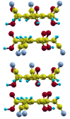
During the growth of the molecular crystal, it might happen that some rings adsorb at each other with the opposite side. In such case, locally, the antiferroelectric phase will form. To estimate the probability of such event, we calculated the 1D molecular wires oriented in: i) the ferroelectric, ii) the totally antiferroelectric (with total dipole moment 0) and iii) the not completely antiferroelectric way (with the total dipole moment lowered with respect to the ferroelectric case but not equal to 0). The two antiferroelectric cases are presented in Figure 8. They differ from each other by a flip of H in the COOH groups. The orientation of the benzene centers in the ferroelectric case (FE) is of the AA-stacking type (one on top of the other). In the antiferroelectric cases (AFE), we rotated one molecule with respect to the other by 30 deg. This rotation does not change the dipole moment along the molecular wire. There is strong electrostatic repulsion within the planes rich of the H atoms and the planes rich of the N and O atoms. For the first geometric conformation, the optimized distances between the central C-rings are 5.51 and 4.89 , for the N-rich and H-rich planes, respectively. The corresponding numbers for the second geometric conformation are 5.55 and 4.85 , respectively. In both cases, the total energy per one molecule of the ferroelectric case is lower than this energy of the antiferroelectric case: i) for the first conformation with vanishing dipole moment, the FE-AFE energy difference is -675 meV and ii) for the the second conformation with a small dipole moment, the corresponding energy difference is -302 meV.
The formation energy , is defined as the difference of the total energies of the whole system and the two subsystems,
| (3) |
For a single molecule on graphene, the formation energy is 1.33 eV for the bottom graphene layer (below the H-rich side of the molecule) and 1.34 eV for the top graphene layer (above the N-rich side of the molecule). The formation of the ferroelectric wire is exotermic with 622 meV per molecule. While for the totally antiferroelectric wire, it is endotermic with 53 meV per molecule. Therefore, the adsorption of the second and next layers on top of graphene will be easier than that of the first layer.
Detailed geometries of the molecule in vacuum, in the wire and on graphene are given in Table 1.
| bond lengths [] | M | M@g | g@M | FE | AFE |
|---|---|---|---|---|---|
| C-ring | 1.405 | 1.434 | 1.434 | 1.405 | 1.412 |
| C-ring-C(OOH) | 1.504 | 1.545 | 1.544 | 1.511 | 1.508 |
| C-ring-C(CN) | 1.527 | 1.525 | 1.524 | 1.523 | 1.528 |
| C-C(N) | 1.468 | 1.422 | 1.421 | 1.460 | 1.465 |
| C-N | 1.163 | 1.269 | 1.268 | 1.165 | 1.165 |
| C-O(H) | 1.370 | 1.389 | 1.390 | 1.358 | 1.376 |
| C-O | 1.215 | 1.171 | 1.170 | 1.218 | 1.209 |
| O-H | 0.984 | 1.004 | 1.004 | 0.986 | 0.987 |
| C-H | 1.102 | 1.151 | 1.150 | 1.100 | 1.104 |
| angles [deg] | M | M@g | g@M | FE | AFE |
| C-C-C(N) | 116.7 | 113.2 | 113.2 | 114.1 | 118.0 |
| C-C-N | 175.9 | 166.1 | 166.2 | 178.4 | 173.3 |
| O-C-O(H) | 123.3 | 128.2 | 128.2 | 124.8 | 122.8 |
IV Conclusions
We have shown that the organic ferroelectric layers with the lateral OH…O bonds display a variety of desired properties for the photovoltaic efficiency. When these layers are the AA-type stacked, they are similar to the columnar clusters with the dipole moment, which were recently proposed as the photovoltaic system without the p-n junction Sobol . Ferroelectricity causes the cascade energy-level alignment of the hole and electron states of the subsequent molecular layers. Importantly, the dipole moments of the layers from the middle of the stack do not cancel, as it is in the bulk ferroelectrics where only the surface dipole moments resist. The fabrication of the presented layers could be done in the presence of the electric field. Such that the ferroelectric (FE), and not the antiferroelectric (AFE), alignment of the neighboring layers is achieved. Statistically, the mixed FE and AFE orderring occurs. However, the AFE orientation is energetically less favourable than the FE one by about 0.30-0.68 eV per molecule, depending on the partial or total vanishing of the dipole moment originating from the COOH and CH2CN groups.
Moreover, the donor or acceptor character of each layer depends on the direction from which
the charge carrier arrives, since this chemical property is defined with
respect to the neighboring layers.
The optically generated hole-electron pair has the character of
the charge-transfer exciton, with an estimated Bohr radius of about 4.7 Å.
The work function of the graphene electrodes, applied to such system, changes due to the
induced surface polarization - and it is about 1.4 eV for the anode and cathode leads,
respectively, when a monolayer of molecules is sandwiched. Functionality of the presented
system can be compared to that of the integrated heterojunctions Bein-2 .
The addition of the electron and hole transport layers is not necessary.
Especially that these systems possess also a property of the separate paths
for the electron and hole transport across the layers our-new .
Acknowledgements
This work has been supported by The National Science Centre of Poland
(the Projects No. 2013/11/B/ST3/04041 and DEC-2012/07/B/ST3/03412).
Calculations have been performed in the Cyfronet Computer Centre, using
Prometheus computer which is a part of the PL-Grid Infrastrucure,
and by part in the Interdisciplinary Centre of
Mathematical and Computer Modeling (ICM).
References
- (1) J. Liu, G. H. Kim, Y. Xue, J. Y. Kim, J. B. Baek, M. Durstock, L. Dai, Adv. Mater., 2014, 26, 786.
- (2) Z.-K. Tan, K. Johnson, Y. Vaynzof, A. A. Bakulin, L.-L. Chua, P. K. H. Ho, R. H. Friend, Adv. Mater., 2013, 25, 4131.
- (3) A. L. Sobolewski, Phys. Chem. Chem. Phys., 2015, 17, 20580.
- (4) D. D. Medina, J. M. Rotter, Y. Hu, M. Dogru, V. Werner, F. Auras, J. T. Markiewicz, P. Knochel and T. Bein, J. Am. Chem. Soc., 2015, 137, 1016.
- (5) M. Calik, F. Auras, L. M. Salonen, K. Bader, I. Grill, M. Handloser, D. D. Medina, M. Dogru, F. Löbermann, D. Trauner, A. Hartschuh, T. Bein, J. Am. Chem. Soc., 2014, 136, 17802.
- (6) Z. Xiao, Y. Yuan, B. Yang, Y. VanDerslice, J. Chen, O. Dyck, G. Duscher, J. Huang, Adv. Mater., 2014, 26, 3068.
- (7) S. Lattante, Electronics, 2014, 3, 132.
- (8) B. Ozyilmaz et al., WO Patent App. PCT/SG2013/000, 2013, 114.
- (9) K. Kim, S.-H. Bae, C. T. Toh, H. Kim, J. H. Cho, D. Whang, T.-W. Lee, B. Özyilmaz, J.-H. Ahn J-H, Appl. Mater. Interfaces, 2014, 6, 3299.
- (10) P. R. Brown, D. Kim, R. R. Lunt, N. Zhao, M. G. Bawendi, J. C. Grossman, V. Bulović, ACS Nano, 2014, 8, 5863.
- (11) P. Giannozzi, S. Baroni, N. Bonini, M. Calandra, R. Car, C. Cavvazzoni, et al., J. Phys. Condens. Matter, 2009, 21, 395502.
- (12) J. P. Perdew, K. Burke, M. Ernzerhof, Phys. Rev. Lett., 1996, 77, 3865.
- (13) D. Vanderbilt, Phys. Rev. B, 1990, 41, R7892.
- (14) A. A. Mostofi, J. R. Yates, Y. S. Lee, I. Souza, D. Vanderbilt, N. Marzari, Comput. Phys. Commun., 2008, 178, 685.
- (15) N. Marzari, D. Vanderbilt, Phys. Rev. B, 1997, 56, 12847.
- (16) N. Marzari, A. A. Mostofi, J. R. Yates, I. Souza, D. Vanderbilt, Rev. Mod. Phys., 2012, 84, 1419.
- (17) L. Andrinopoulos, N. D. M. Hine, A. A. Mostofi, J. Chem. Phys., 2011, 135, 154105.
- (18) K. Z. Milowska, M. Wierzbowska, Chem. Phys., 2014, 430, 7.
- (19) R. Resta, Rev. Mod. Phys., 1994, 66, 899.
- (20) M. Gibertini, G. Pizzi, N. Marzari, Nature Commun., 2014, 5, 5157.
- (21) S. Horiuchi, R. Kumai, Y. Tokura, J. Am. Chem. Soc., 2013, 135, 4492.
- (22) S. Horiuchi, K. Kobayashi, R. Kumai, S. Ishibashi, Chem. Lett. (Highlight Review), 2014, 43, 26.
- (23) X. Zhu, N. R. Monahan, Z. Gong, H. Zhu, K. W. Williams, C. A. Nelson, J. Am. Chem. Soc., 2015, 137, 8313.
- (24) S. Suzuki, C. Bower, Y. Watanabe, O. Zhou, Appl. Phys. Lett., 2000, 76, 4007.
- (25) Y.-J. Yu, Y. Zhao, S. Ryu, L. E. Brus, K. S. Kim, P. Kim, Nano Lett., 2009, 9, 3430.
- (26) K. T. Chan, J. B. Neaton, M. L. Cohen, Phys. Rev. B, 2008, 77, 235430.
- (27) M. Khazaei, M. Arai, T. Sasaki, A. Ranjbar, Y. Liang, S. Yunoki, Phys. Rev. B, 2015, 92, 075411.
- (28) W. E. Ford, D. Gao, N. Knorr, R. Wirtz, F. Scholz, Z. Karipidou, K. Ogasawara, S. Rosselli, V. Rodin, G. Nelles, F. von Wrochem, ACS Nano, 2014, 8, 9173.
- (29) E. Wigner and J. Bardeen, Phys. Rev., 1935, 48, 84.
- (30) T. C. Leung, C. L. Kao, W. S. Su, Y. J. Feng, C. T. Chan, Phys. Rev. B, 2003, 68, 195408.
- (31) M. Wawrzyniak-Adamczewska and M. Wierzbowska, J. Phys. Chem. C, 2016, 120, 7748.