Control of excitons in multi-layer van der Waals heterostructures
Abstract
We report an experimental study of excitons in a double quantum well van der Waals heterostructure made of atomically thin layers of MoS2 and hexagonal boron nitride (hBN). The emission of neutral and charged excitons is controlled by gate voltage, temperature, and both the helicity and the power of optical excitation.
pacs:
73.21.Ac, 71.35.Cc, 71.35.Pq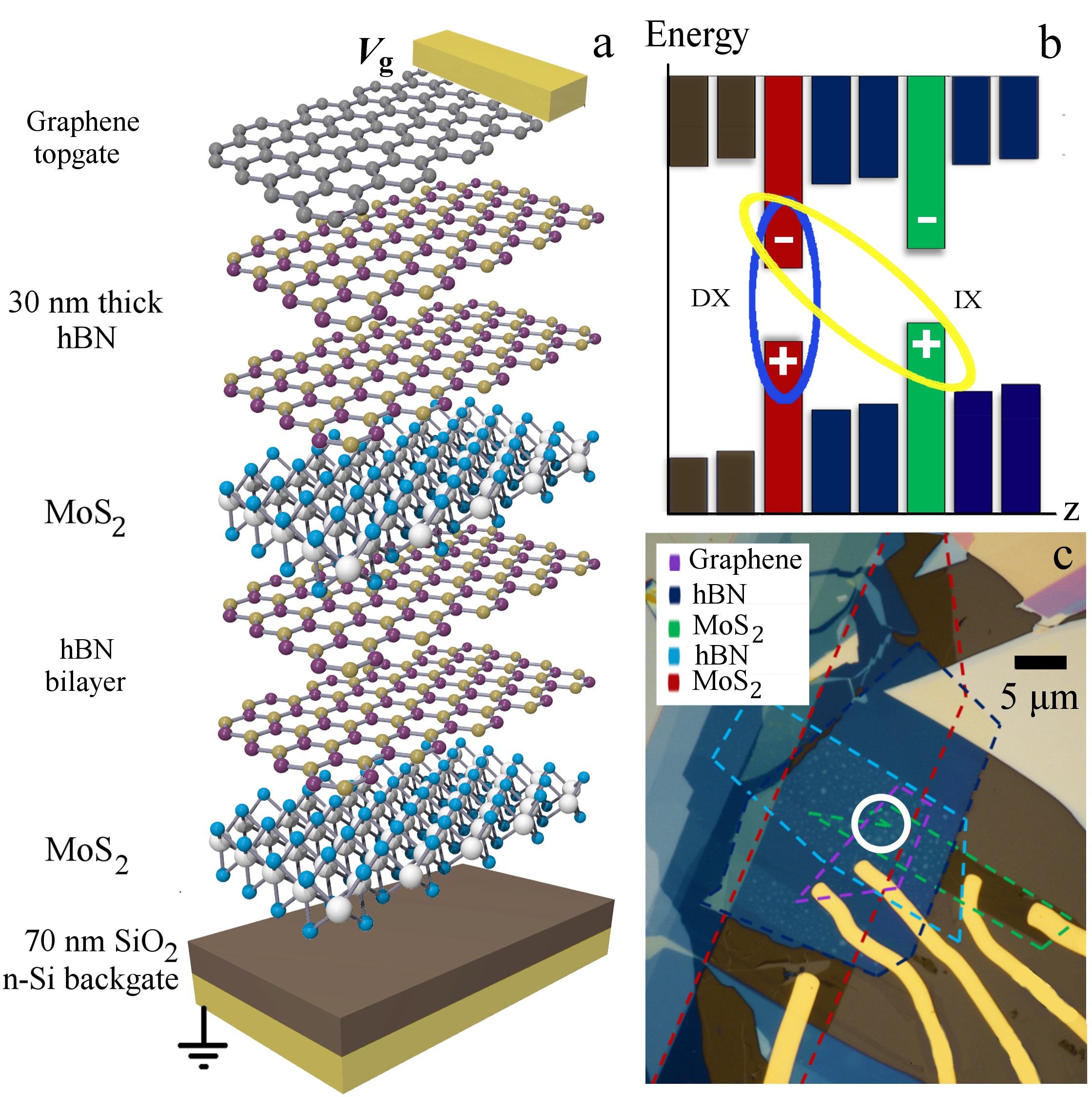
Van der Waals heterostructures composed of ultrathin layers of transition metal dichalcogenides (TMD), such as MoS2, WSe2, etc., offer an opportunity to realize artificial materials with designable properties, forming a new platform for studying basic phenomena and developing optoelectronic devices Geim and Grigorieva (2013). In TMD structures, excitons have high binding energies and are prominent in the optical response. The energy, intensity, and polarization of exciton emission gives information about electronic, spin, and valley properties of TMD materials Splendiani et al. (2010); Mak et al. (2010); Zeng et al. (2012); Mak et al. (2012); Cao et al. (2012); Cheiwchanchamnangij and Lambrecht (2012); Ramasubramaniam (2012); Wu et al. (2013); Mak et al. (2013); Ross et al. (2013); Berkelbach et al. (2013); Shi et al. (2013); Qiu et al. (2013); Ye et al. (2014); Chernikov et al. (2014); Xu et al. (2014); Fang et al. (2014); Cheng et al. (2014); Zhang et al. (2014); Rivera et al. (2015); Qiu et al. (2015); Palummo et al. (2015).
Exciton phenomena are expected to become even richer in structures that contain two 2D layers. The energy-band diagram of such a coupled quantum well (CQW) structure is shown schematically in Figure 1b. Previous studies of GaAs Islam et al. (1987), AlAs Zrenner et al. (1992), and InGaAs Butov et al. (1995) CQWs showed that excitons in these structures can be effectively controlled by voltage and light. Two types of excitons are possible in a CQW structure. Spatially direct excitons (DXs) are composed of electrons and holes in the same layer, while indirect excitons (IXs) are bound states of electrons and holes in the different layers separated by a distance , Figure 1b. IXs can form quantum degenerate Bose gases Lozovik and Yudson (1976); Fukuzawa et al. (1990). The realization and control of quantum IX gases was demonstrated High et al. (2008, 2012) in GaAs CQW structures at temperatures below a few degrees Kelvin. In a recent theoretical work Fogler et al. (2014) it was predicted that the large exciton binding energies in TMD CQW structures may bring the domain of these phenomena to high temperatures. On the other hand, DXs in TMD CQW structures have a high oscillator strength making these structures good emitters Splendiani et al. (2010); Mak et al. (2010); Zeng et al. (2012); Mak et al. (2012); Cao et al. (2012); Cheiwchanchamnangij and Lambrecht (2012); Ramasubramaniam (2012); Wu et al. (2013); Mak et al. (2013); Ross et al. (2013); Berkelbach et al. (2013); Shi et al. (2013); Qiu et al. (2013); Ye et al. (2014); Chernikov et al. (2014); Xu et al. (2014); Fang et al. (2014); Cheng et al. (2014); Zhang et al. (2014); Rivera et al. (2015); Qiu et al. (2015); Palummo et al. (2015). CQW structures allow control of the exciton emission by voltage. These properties make CQW structures an interesting new system for studying exciton phenomena in TMD materials.
The DX binding energy is larger Fogler et al. (2014) than that of the IXs, so in the absence of an external field the DXs are lower in energy. The electric field normal to the layers induces the energy shift of IXs. The transition between the direct regime where DXs are lower in energy to the indirect regime where IXs are lower in energy occurs when Butov et al. (1995). Both direct and indirect regimes show interesting exciton phenomena. The indirect regime was considered in earlier studies of GaAs Islam et al. (1987), AlAs Zrenner et al. (1992), InGaAs Butov et al. (1995), and TMD Fang et al. (2014); Rivera et al. (2015) CQW structures. The direct regime in TMD CQW structures is considered in this work. Exploring the direct regime is essential for understanding both the universal properties of complex exciton systems in CQW structures and the specific properties of direct excitons in TMD layers. We found that the exciton spectra in the direct regime have three exciton emission lines. The ability to control the CQW structure by voltage provides an important tool for understanding the complex exciton emission in TMD structures. The measured dependence of exciton spectra on voltage, temperature and excitation indicated that the lines correspond to the emission to neutral and charged excitons.
The structure studied here was assembled by stacking mechanically exfoliated layers on a Si/SiO2 substrate, which acts as a global backgate (Figure 1a). The top view of the device showing the contours of different layers is presented in Figure 1c. The CQW is formed where the two MoS2 monolayers, separated by an hBN bilayer, overlap. The upper – thick hBN served as a dielectric cladding layer for a top graphene electrode. Voltage applied between the top graphene layer and a backgate was used to create the bias across the CQW structure.
The excitons were generated by continuous wave (cw) semiconductor lasers with excitation energies , , or focused to a spot of diameter (the circle in Figure 1b). The photoluminescence (PL) spectra were measured using a spectrometer with resolution and a CCD. In time-resolved PL measurements excitons were generated by a pulsed semiconductor laser with and the emitted light was diffracted by the spectrometer and detected by a photomultiplier tube and time correlated photon counting system. The measurements were performed in a 4He cryostat.
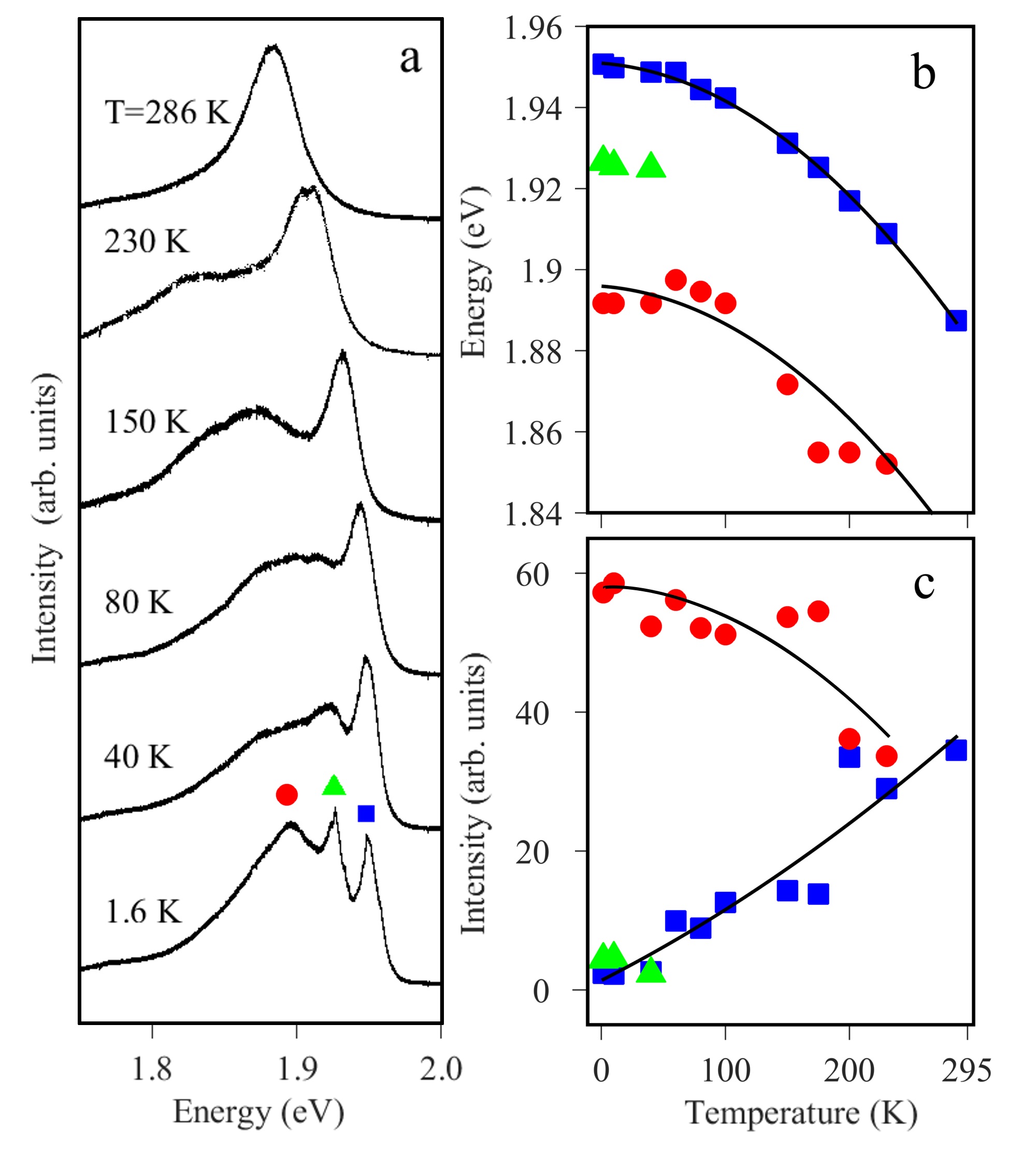
Figure 2 shows the PL spectra at different temperatures . At the lowest , the spectrum consists of two high-energy emission lines with the linewidth and a broader low-energy line. Additional data and analysis presented below suggest that the high-energy lines correspond to the emission of neutral DXs while the low-energy line to the emission of charged DXs also known as trions.
The energy splitting of between the high-energy emission lines constitutes only of the MoS2 exciton binding energy Cheiwchanchamnangij and Lambrecht (2012); Ramasubramaniam (2012); Berkelbach et al. (2013); Shi et al. (2013); Qiu et al. (2013); Ye et al. (2014); Chernikov et al. (2014); Zhang et al. (2014); Qiu et al. (2015) of about . It is also much smaller than energy difference of the and excitons Mak et al. (2010) caused by the spin-orbit splitting of the valence band (see Figure 4c). These data indicate that the high-energy lines represent different species of excitons. They can be excitons with different electron spin states. The calculated difference Kormányos et al. (2014) in the masses, vs. , of the conduction band spin states results in a difference in the reduced electron-hole masses and, in turn, exciton binding energies. This leads to the energy splitting consistent with the experiment.
It is worth noting that the two MoS2 layers in the structure have inequivalent dielectric environment (Figure 1). This may lead to the difference in the binding energy of excitons in these layers in the effective mass approximation Sup . However, experimental and theoretical studies show that the TMD excitonic states with large binding energy are robust to environmental perturbations Ye et al. (2014), meaning the exciton energy is the same for the two MoS2 layers in the structure.
The lower-energy emission line is shifted by about from the first two (Figure 2). This shift is in the range, –, of trion binding energies reported Mak et al. (2012, 2013); Ross et al. (2013); Berkelbach et al. (2013) for monolayer MoS2. The relative intensity of the high-energy exciton lines increases with (Figure 2), which is consistent with thermal dissociation of trions. The observed red shift of the lines with increasing temperature originates from the band gap reduction, which is typical in semiconductors,Varshni (1967) the TMDs included Korn et al. (2011); Ross et al. (2013); Soklaski et al. (2014); Zhang et al. (2014).
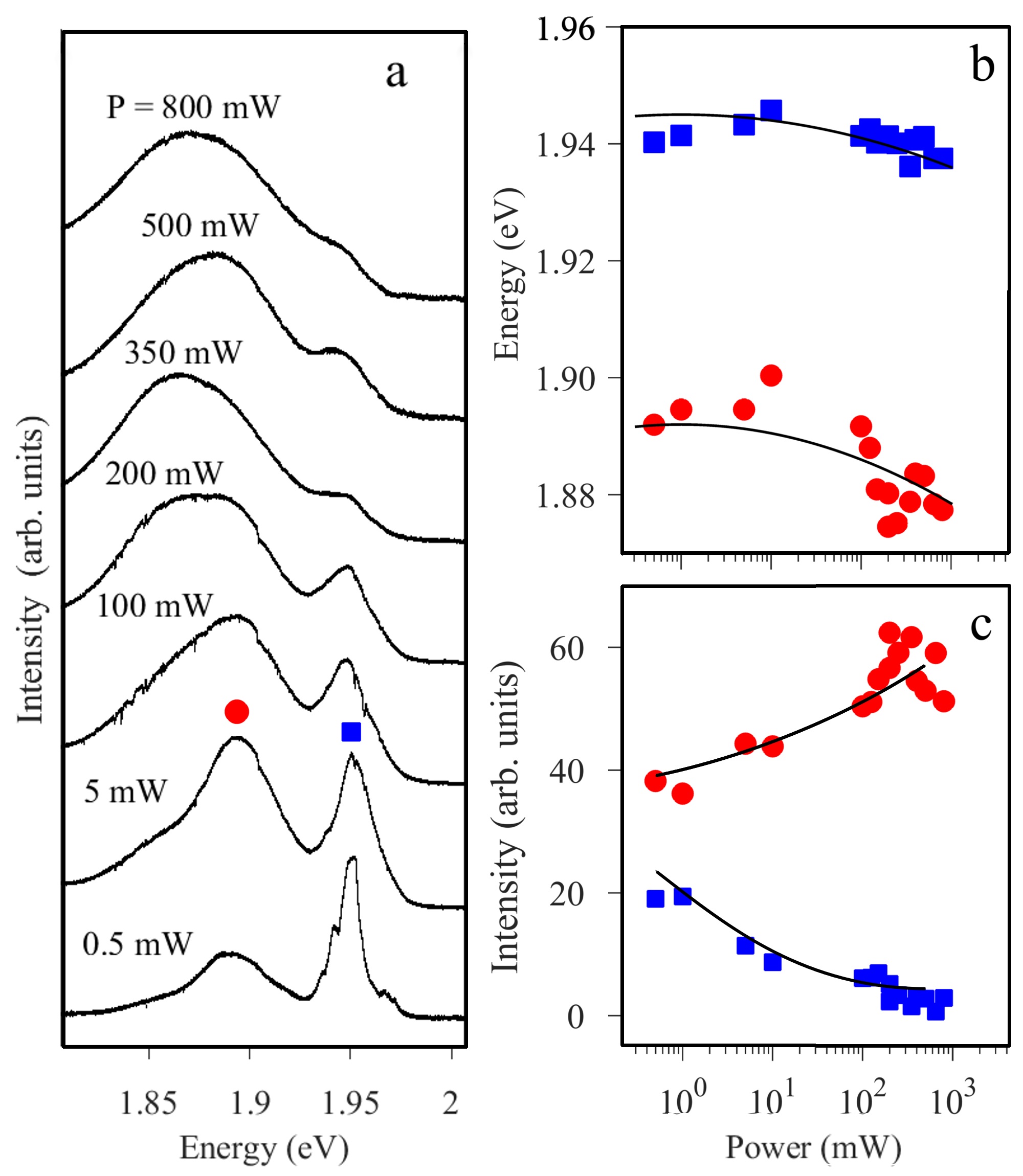
Figure 3 shows the dependence of the exciton PL on the excitation power . The relative intensity of the trion line increases with (Figure 3). This effect may be due to an enhanced probability of trion formation at larger carrier density. A similar increase of the trion PL intensity relative to the exciton was observed in earlier studies of GaAs CQW structures Butov et al. (2001).
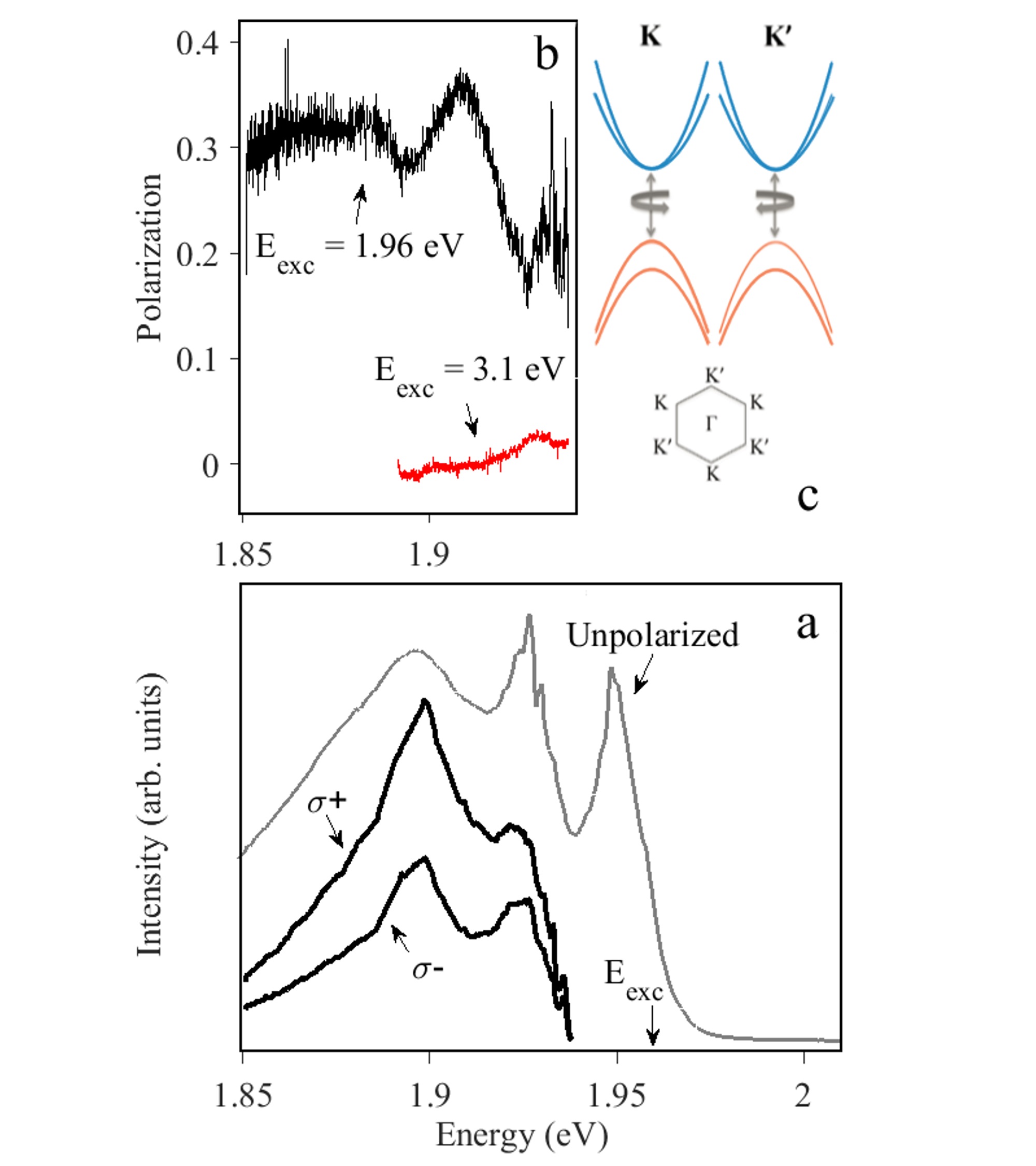
Figure 4 shows that the polarization of exciton emission can be controlled by the helicity of optical excitation. For a circularly polarized excitation nearly resonant with the exciton line, a high degree of circular polarization of exciton PL is observed (Figure 4a,b) which is consistent withstudies of monolayer TMD Zeng et al. (2012); Mak et al. (2012); Cao et al. (2012); Wu et al. (2013); Xu et al. (2014). This observation indicates that the spin relaxation time is long compared to the exciton recombination and energy relaxation times Maialle et al. (1993). The conventional explanation for the slow spin relaxation of excitons invokes spin-orbit coupling (SOC) and spin-valley coupling effects. As illustrated in Figure 4c, the SOC splits valence band of the MoS2 monolayers, leading to the appearance of the aforementioned and exciton states. The excitons are higher in energy and their contribution to the PL is negligible. The excitons can come from either or valley. It is important however that the spin and valley indices are coupled, so that exciton spin relaxation requires inter-valley scattering (Figure 4c). If this scattering is weak, the spin relaxation can be long. Virtually no circular polarization is observed for nonresonant optical excitation (Figure 4b), indicating that the high-energy photoexcited carriers loose their spin polarization during energy relaxation. Our time-resolved PL measurements revealed that the exciton and trion lifetimes are short, shorter than the resolution of the photon counting system. Such small lifetimes facilitate the realization of the regime where the spin relaxation time is long compared to the exciton recombination time, and therefore, the polarization of exciton emission remains high.
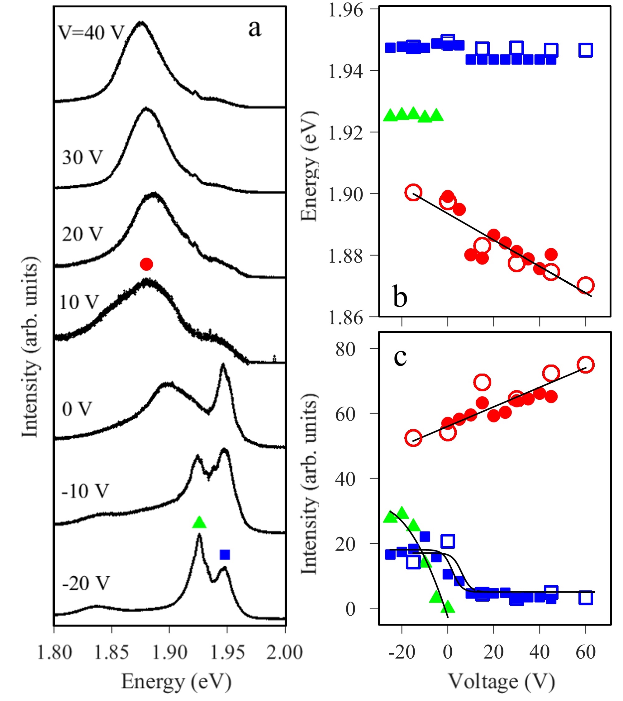
Figure 5 shows the gate-voltage dependence of the exciton PL. The small exciton lifetime indicates the direct regime in the studied range of voltage because the IX lifetimes are expected to be in the ns range. Fogler et al. (2014); Rivera et al. (2015); Fang et al. (2014); Palummo et al. (2015) The positions of the exciton lines remain essentially unchanged while the trion line exhibits a red shift with the slope per of . The smallness of the shifts of the lines corroborates the conclusion that the CQW is in the direct regime. Indeed, if we assume that the electric field in the device is uniform, the IX energy shift with voltage should be . The main effect of the gate voltage in the direct regime is the control of the exciton and trion PL intensities: the high-energy exciton emission increased at negative , while the low-energy trion emission increased at positive (Figure 5). This behavior is attributed by the voltage-dependent electron concentration in the MoS2 layers. The initial electron concentration at arises from unintentional dopants typically present in MoS2 materials. The change of as a function of can be estimated from simple electrostatics. Treating the CQW as a single unit and neglecting a minor contribution from quantum capacitance, we find
| (1) |
where , are the geometric capacitances and leakage resistances of the dielectrics above (below) this double layer. (Incidentally, the leakage current across the device did not exceed a few until an eventual breakdown of the device at .) Since generally , the applied voltage changes and, as a result, modifies the concentration of trions relative to neutral excitons.
In summary, we presented optical studies of excitons in a MoS2 coupled quantum well van der Waals heterostructure. We observed three emission lines. The dependence of these lines on experimental parameters indicates that the two high energy lines correspond to the emission of neutral excitons and the lowest energy line to the emission of charged excitons (trions). We demonstrated control of the exciton emission by gate voltage, temperature, and also by the helicity and power of optical excitation.
This work was supported by the U.S. Department of Energy, Office of Basic Energy Sciences under award DE-FG02-07ER46449. M.M.F. was supported by the Office of the Naval Research. Work at the University of Manchester was supported by the European Research Council and the Royal Society.
References
- Geim and Grigorieva (2013) A. K. Geim and I. V. Grigorieva, Nature 499, 419 (2013).
- Splendiani et al. (2010) A. Splendiani, L. Sun, Y. Zhang, T. Li, J. Kim, C.-Y. Chim, G. Galli, and F. Wang, Nano Lett. 10, 1271 (2010).
- Mak et al. (2010) K. F. Mak, C. Lee, J. Hone, J. Shan, and T. F. Heinz, Phys. Rev. Lett. 105, 136805 (2010).
- Zeng et al. (2012) H. Zeng, J. Dai, W. Yao, D. Xiao, and X. Cui, Nature Nanotech. 7, 490 (2012).
- Mak et al. (2012) K. F. Mak, K. He, J. Shan, and T. F. Heinz, Nature Nanotech. 7, 494 (2012).
- Cao et al. (2012) T. Cao, G. Wang, W. Han, H. Ye, C. Zhu, J. Shi, Q. Niu, P. Tan, E. Wang, B. Liu, and J. Feng, Nat. Commun. 3, 887 (2012).
- Cheiwchanchamnangij and Lambrecht (2012) T. Cheiwchanchamnangij and W. R. L. Lambrecht, Phys. Rev. B 85, 205302 (2012).
- Ramasubramaniam (2012) A. Ramasubramaniam, Phys. Rev. B 86, 115409 (2012).
- Wu et al. (2013) S. Wu, J. S. Ross, G.-B. Liu, G. Aivazian, A. Jones, Z. Fei, W. Zhu, D. Xiao, W. Yao, D. Cobden, and X. Xu, Nature Phys. 9, 149 (2013).
- Mak et al. (2013) K. F. Mak, K. He, C. Lee, G. H. Lee, J. Hone, T. F. Heinz, and J. Shan, Nature Mater. 12, 207 (2013).
- Ross et al. (2013) J. S. Ross, S. Wu, H. Yu, N. J. Ghimire, A. M. Jones, G. Aivazian, J. Yan, D. G. Mandrus, D. Xiao, W. Yao, and X. Xu, Nat. Commun. 4, 1474 (2013).
- Berkelbach et al. (2013) T. C. Berkelbach, M. S. Hybertsen, and D. R. Reichman, Phys. Rev. B 88, 045318 (2013).
- Shi et al. (2013) H. Shi, H. Pan, Y.-W. Zhang, and B. I. Yakobson, Phys. Rev. B 87, 155304 (2013).
- Qiu et al. (2013) D. Y. Qiu, F. H. da Jornada, and S. G. Louie, Phys. Rev. Lett. 111, 216805 (2013).
- Ye et al. (2014) Z. Ye, T. Cao, K. O’Brien, H. Zhu, X. Yin, Y. Wang, S. G. Louie, and X. Zhang, Nature 513, 214 (2014).
- Chernikov et al. (2014) A. Chernikov, T. C. Berkelbach, H. M. Hill, A. Rigosi, Y. Li, O. B. Aslan, D. R. Reichman, M. S. Hybertsen, and T. F. Heinz, Phys. Rev. Lett. 113, 076802 (2014).
- Xu et al. (2014) X. Xu, W. Yao, D. Xiao, and T. F. Heinz, Nature Phys. 10, 343 (2014).
- Fang et al. (2014) H. Fang, C. Battaglia, C. Carraro, S. Nemsak, B. Ozdol, J. S. Kang, H. A. Bechtel, S. B. Desai, F. Kronast, A. A. Unal, G. Conti, C. Conlon, G. K. Palsson, M. C. Martin, A. M. Minor, C. S. Fadley, E. Yablonovitch, R. Maboudian, and A. Javey, PNAS 111, 6198 (2014).
- Cheng et al. (2014) R. Cheng, D. Li, H. Zhou, C. Wang, A. Yin, S. Jiang, Y. Liu, Y. Chen, Y. Huang, and X. Duan, Nano Lett. 14, 5590 (2014).
- Zhang et al. (2014) C. Zhang, H. Wang, W. Chan, C. Manolatou, and F. Rana, Phys. Rev. B 89, 205436 (2014).
- Rivera et al. (2015) P. Rivera, J. R. Schaibley, A. M. Jones, J. S. Ross, S. Wu, G. Aivazian, P. Klement, K. Seyler, G. Clark, N. J. Ghimire, J. Yan, D. G. Mandrus, W. Yao, and X. Xu, Nat. Commun. 6, 6242 (2015).
- Qiu et al. (2015) D. Y. Qiu, F. H. da Jornada, and S. G. Louie, Phys. Rev. Lett. 115, 119901 (2015).
- Palummo et al. (2015) M. Palummo, M. Bernardi, and J. C. Grossman, Nano Lett. 15, 2794 (2015).
- Islam et al. (1987) M. N. Islam, R. L. Hillman, D. A. B. Miller, D. S. Chemla, A. C. Gossard, and J. H. English, Appl. Phys. Lett. 50, 1098 (1987).
- Zrenner et al. (1992) A. Zrenner, P. Leeb, J. Schäfer, G. Böhm, G. Weimann, J. M. Worlock, L. T. Florez, and J. P. Harbison, Surf. Sci. 263, 496 (1992).
- Butov et al. (1995) L. V. Butov, A. Zrenner, G. Abstreiter, A. V. Petinova, and K. Eberl, Phys. Rev. B 52, 12153 (1995).
- Lozovik and Yudson (1976) Y. E. Lozovik and V. I. Yudson, Sov. Phys. JETP 44, 389 (1976).
- Fukuzawa et al. (1990) T. Fukuzawa, S. Kano, T. Gustafson, and T. Ogawa, Surf. Sci. 228, 482 (1990).
- High et al. (2008) A. A. High, E. E. Novitskaya, L. V. Butov, M. Hanson, and A. C. Gossard, Science 321, 229 (2008).
- High et al. (2012) A. A. High, J. R. Leonard, A. T. Hammack, M. M. Fogler, L. V. Butov, A. V. Kavokin, K. L. Campman, and A. C. Gossard, Nature 483, 584 (2012).
- Fogler et al. (2014) M. M. Fogler, L. V. Butov, and K. S. Novoselov, Nat. Commun. 5, 4555 (2014).
- Kormányos et al. (2014) A. Kormányos, V. Zólyomi, N. D. Drummond, and G. Burkard, Phys. Rev. X 4, 011034 (2014).
- (33) See supplemental material at [URL will be inserted by AIP] for estimates of the exciton binding energies.
- Varshni (1967) Y. Varshni, Physica 34, 149 (1967).
- Korn et al. (2011) T. Korn, S. Heydrich, M. Hirmer, J. Schmutzler, and C. Schüller, Appl. Phys. Lett. 99, 102109 (2011).
- Soklaski et al. (2014) R. Soklaski, Y. Liang, and L. Yang, Appl. Phys. Lett. 104, 193110 (2014).
- Butov et al. (2001) L. V. Butov, A. Imamoglu, K. L. Campman, and A. C. Gossard, J. Exp. Theor. Phys. 92, 260 (2001).
- Maialle et al. (1993) M. Z. Maialle, E. A. de Andrada e Silva, and L. J. Sham, Phys. Rev. B 47, 15776 (1993).