A Clock Synchronizer for Repeaterless Low Swing On-Chip Links
Abstract
A clock synchronizing circuit for repeaterless low swing interconnects is presented in this paper. The circuit uses a delay locked loop (DLL) to generate multiple phases of the clock, of which the one closest to the center of the eye is picked by a phase detector loop. The picked phase is then further fine tuned by an analog voltage controlled delay to position the sampling clock at the center of the eye. A clock domain transfer circuit then transfers the sampled data to the receiver clock domain with a maximum latency of three clock cycles. The proposed synchronizer has been designed and fabricated in 130 nm UMC MM CMOS technology. The circuit consumes 1.4 mW from a 1.2 V supply at a data rate of 1.3 Gbps. Further, the proposed synchronizer has been designed and simulated in TSMC 65 nm CMOS technology. Post layout simulations show that the synchronizer consumes 1.5 mW from a 1 V supply, at a data rate of 4 Gbps in this technology.
Index Terms:
Current mode interconnects, Low swing interconnect, repeater insertion, clock data recovery, Mesochronous synchronizers.I Introduction
It has been well established that the performance of digital processing systems is limited by the throughput and power consumption of global interconnects [1, 2, 3, 4]. Repeater insertion alleviates this problem to some extent, but it increases the power consumption of the link, while also bringing in additional constraints in placement and routing. These limitations have resulted in a lot of interest in repeaterless low swing interconnects, with equalization at the transmitter [5, 6, 7] or receiver [8] or both [9], to improve the speed, while keeping the power consumption low. The receiver circuit for low swing interconnects is a comparator which converts the received low swing signal to CMOS levels. To keep the power consumption and latency low, regenerative clocked comparators are used [10, 7, 11].
While low swing interconnects help maximize the throughput of long interconnects, the latency of the interconnects is still high and can be as high as multiple cycles. This is the case even for transmission line based interconnects that operate at the theoretical minimum latency [12]. Conventional repeater inserted interconnects use synchronizing flip-flops at section lengths less then the critical path delay of the full chip to maintain synchronization [13]. Inserting synchronizing flip-flops along a low swing line will however mean that the improvements offered by repeaterless links will not be leveraged to full potential. Hence, a clock re-timing circuit that ensures that the data is sampled at the center of the eye is required. Further, the resolved data should be transferred to the receiver clock domain with an appropriate synchronizer. This problem, despite being serious, has not received much attention in the literature.
Fig. 1 shows a block diagram of a typical low swing interconnect system.
Here, is the transmitter clock, is the receiver clock, and is the desired sampling clock with its active edge at the center of the data eye. The delay of the repeaterless interconnect, that must be compensated for, is expressed as , where is the system clock period, is a positive integer (including 0), and is a positive real number which is less than 1. Mensink et al. in [10] estimate the delay using extracted simulations of the interconnect and add appropriate delay at design time itself. This needs sufficient over design so as to ensure proper operation at the desired frequency across process corners. Source synchronous schemes, akin to the one described in [14], are not compatible with low swing interconnects as converting the low swing clock to full swing clock will need buffers, whose delay again cannot be predicted accurately at design time.
Clock and data recovery (CDR) circuits have been reported for off chip interconnects, and are well known [15]. These circuits are typically phase locked loops that lock a local oscillator’s frequency to the incoming data frequency. However, for on-chip interconnects, only the phase needs to be recovered and a clock running at the correct frequency is available at the receiver. Fig. 2 shows the concept of such a clock recovery circuit.
Here a phase detector senses the phase error between the data and the clock and generates an error signal. The integrated error signal controls a delay circuit that delays the sampling clock. The negative feedback minimizes the error, resulting in the sampling clock position at the center of the eye. Lee et al. in [9] report a source synchronous link that uses a digitally controlled delay line in the clock path at the receiver, which is trained in calibration mode before the interconnect is used. For calibration, 0.5 unit interval delay is inserted at the transmitter and a pattern toggling between 1 and 0 is sent. The receiver clock delay is then swept to find the crossing over of the data and clock edges, and after completion of training, the 0.5 unit interval delay is removed. This however means that the technique cannot be extended to adaptive synchronizers. Also, the accuracy is limited by the phase quantization error. If a conventional phase detector like the Alexander phase detector is used, the delay line should be initialized to the center of the range, due to its finite range. While infinite phase delay can be accomplished using phase interpolators as reported in [16], the circuit is predominantly analog and complex, making it likely to suffer from mismatch in scaled technologies. Another limitation of analog circuits is that their state cannot be easily saved for fast initialization on subsequent power ups.
In this work, we present a fast automatic synchronizer that is adaptive and does not have the limitations mentioned above. The circuit is built around a DLL that generates multiple phases of the clock. A phase detector loop picks the DLL phase closest to the center of the eye. In order to reduce the phase quantization error, an analog delay line is used to fine tune the selected clock phase so as to position it at the center of the data eye. A similar concept has been used for clock synthesis in [17, 18], in which a coarse DLL generates multiple phases of the clock, which are delayed by multiple delay lines or interpolated to obtain the clock of the correct phase. However these techniques are reported for clock synthesis and not for clock and data recovery, and either use multiple VCDL’s [17] or use digital fine tuning which causes jitter due to dithering. The proposed technique uses a much simpler implementation with only one VCDL.
Once sampled, the data must then be transferred to the receiver clock domain. Serial synchronizers with two or more flip-flops are typically used for such clock domain transfers [19], which however bring a penalty in latency. In the design described here, using one of the phases of the DLL, a low latency clock domain transfer to the receiver clock domain has been implemented.
The paper is organized as follows. Section II describes the architecture of the clock synchronizer. Clock domain transfer, from the sampling clock domain to the receiver clock domain, is described in section III. Jitter analysis is presented in section IV which is followed by a discussion on implementation and results in Section V. Section VI concludes this paper. Appendix A discusses an anomaly in DLL based clock recovery circuits using the Alexander phase detector.
II Clock recovery circuit
Fig. 3LABEL:sub@fig:CPA_analog shows a block diagram of the proposed clock synchronizing circuit. It consists of a coarse tuning loop and a fine tuning loop. The main component of fine tuning loop is a voltage controlled delay line (VCDL) that provides a controllable delay to the clock. The main component of the coarse tuning loop is a DLL that generates multiple phases of the clock, of which the one closest to the center of the data eye is picked by the control loop. Since the system is of the first order, the loop filter is a single capacitor, as shown between the fine and coarse tuning loops in Fig. 3LABEL:sub@fig:CPA_analog.
Operation of the circuit starts with the fine tuning loop trying to get the clock to the center of the data eye, by delaying the clock using the VCDL. If the entire VCDL range is spent before lock is achieved (which is identified by the control voltage exceeding preset bounds), the coarse tuning loop is woken up to pick the next phase of the DLL as the source clock and the control voltage is reset to lie within the window. This process repeats until the phase closest to the center of the eye is selected and the VCDL range is sufficient to lock the clock to the exact center of the eye.
Referring to Fig. 3LABEL:sub@fig:CPA_analog, the input low swing data first goes to a phase detector. The and pulses from the phase detector are averaged using a weak charge pump. The averaged control voltage () then modulates the delay of the VCDL. The VCDL source clock comes from the coarse tuning loop, and is one of the phases of the DLL. The VCDL is designed to have a range greater than 1 phase step of the DLL.
In the coarse tuning loop, a window comparator senses the control voltage () and if it exceeds a predetermined range (which is the range of the control voltage for the VCDL in the fine tuning loop), it triggers the logic block. The logic block is an FSM that generates the and signals for the one hot ring counter (shown in Fig. 3LABEL:sub@fig:ring_counter). The state of the ring counter is used to select one of the phases of the clocks generated by the DLL. The direction in which the ring counter counts depends on whether the control voltage exceeds the upper threshold or is below the lower threshold of the window comparator. Whenever the window thresholds are crossed, a secondary strong charge pump resets the control voltage () to bring it within the window. When the control voltage is within the window thresholds, the digital circuits retain their state by de-asserting the signal.
Fig. 4LABEL:sub@fig:vc shows the trajectory of the control voltage from start-up to lock condition. Fig. 4LABEL:sub@fig:Qs shows the progression of the ring counter from reset state to locked state.
Fig. 5 shows the simulated eye diagram of the data and the clock after lock has been achieved.
Fig. 6 shows the diagram of the window comparator and the logic which controls the strong charge pump.
The comparators used in this circuit are traditional static comparators [20]. The comparators trip when the control voltage crosses the preset thresholds. The clock for this circuit is obtained by dividing the system clock by a factor . The clock is divided to make the speed acceptable for the digital logic and the strong charge pump, in addition to saving power. The ring counter is enabled only if any one of the comparator’s outputs is high. This happens only when the control voltage is not within the allowed range. The signal for the ring counter, and & signals for the strong charge pump are derived from the comparator outputs. When is more than the upper threshold (), is high. At this time the upper flip-flop is enabled. On the next clock after this event, the ring counter counts down and in order to bring within the window, the signal for the strong charge pump is asserted. Once the loop filter capacitor discharges sufficiently so that is within the window comparator thresholds, the comparator outputs go low. This resets the flip-flops and de-asserts . Depending on the chosen clock division ratio , the strong charge pump is designed such that this exercise is completed in one cycle, taking into consideration the time taken by the comparators to resolve. Similar process follows when is less than the lower threshold (), when the ring counter counts up. The ring counter state can be captured in a snapshot register and used to initialize the counter for locking the loop quickly at subsequent power up.
III Clock domain transfer
Once the data has been sampled with a synchronized clock and converted to CMOS levels, it should be re-timed to the receiver clock domain. Typically, multi flip-flop serial synchronizers are used for this. Since multiple clock phases are already available in the design described here, the clock domain transfer can be performed with a single flip-flop that is clocked with an intermediate phase. Fig. 7 shows the serial synchronizer along with the clock domain transfer flip-flop.
Here the DLL generates phases of the clock. The clock recovery system selects the phase closest to the center of the data () and delays it appropriately, to generate such that it is positioned at the center of the eye. The retimed data from the phase detector is available at this phase . The receiver samples the data at the receiver clock which is (which is same as of the DLL). The flip-flop should be clocked with a phase that will guarantee that no flip-flop samples during a data transition. is selected as
| otherwise. |
Fig. 8 shows the sampling clocks for the worst case latency, for an example case that uses an 8 phase DLL (). One can see that . Using simplifies the implementation in two ways. First, it reduces the load on the DLL and switch matrix. In addition, it also compensates for the delay introduced by the clock buffers from switch matrix output to the phase detector’s clock input, with the delay introduced in generating from .
Here, an assumption that a flip-flop sampling a valid data input is able to resolve its output in time is made. Since pipelined microprocessors generally have a logic depth of more than 5 NAND gates, this assumption is not very demanding. The reason for choosing for comes from the fact that the fine tuning loop of the clock recovery system could delay the sampling clock by at most 2 phase steps of the DLL. This is because the VCDL is overdesigned for two phase steps so as to meet the range requirements across process corners. This is explained later in section V when discussing the VCDL.
The total latency of the above synchronizer is at most 3 clock cycles. The phase detector takes 2 clock cycles (as will be explained in section V) and the following DFF’s output is sampled half a clock cycle later. Under the worst conditions the third flip-flop in the chain will introduce another half a clock cycle delay. This makes the total latency .
IV Jitter Analysis
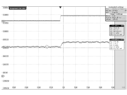
Clock recovery circuits that use the data transitions to estimate the correct sampling phase are generally sensitive to the jitter in the received data. The jitter in the received data comes due to the phase noise in the transmitter clocks which is random in nature, and due to ISI in the channel, which is deterministic. Also, wander in the clock generating oscillators results in low frequency jitter. Typically, clock recovery circuits are required to tolerate small amplitude of high frequency jitter (typically under 0.1 unit interval (UI)) and large amplitude of low frequency jitter (up to 0.5 UI or more). However, the synchronizer for the application of repeaterless on-chip interconnect system discussed in this paper, does not need to be tolerant to the low frequency jitter. This is because the transmitter and the receiver share the same clock source albeit in arbitrary phase relationship. To verify this the synchronizer was tested with a low frequency jitter of 1 MHz frequency and 0.5 UI amplitude. In order to reduce the simulation time, first, extracted layout of the DLL alone was simulated with an input clock having low frequency jitter, which confirmed that the DLL clock phases tracked the low frequency jitter. Then the full loop of the synchronizer with the schematic level netlists and an ideal DLL model was simulated. Fig. 9 shows the eye diagram of the received data with jitter, and the control voltage for this simulation. As the low frequency jitter is correlated between the transmitter and the receiver, the control voltage does not have to track it.
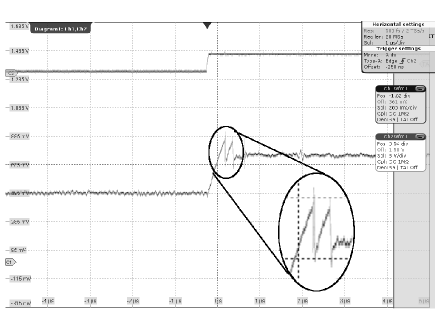
High frequency jitter which is generated in the clock distribution networks due to thermal noise in transistors and power supply noise will however not be common to the transmitter and receiver. This high frequency jitter is however filtered out by the filter capacitor in the synchronizer circuit. Fig. 10 shows the eye diagram and control voltage for a sinusoidal jitter of an amplitude of 0.1 UI at a frequency of 50 MHz. The circuit was also simulated for high frequency uncorrelated jitter of 50 MHz and 200 MHz for 10 with various jitter amplitudes. The circuit has no errors even for jitter amplitudes as high as 0.4 UI.
In conclusion for an acceptable level of low frequency jitter tolerance, the DLL in the synchronizer must be designed with a loop bandwidth that is more as compared to the expected low frequency jitter in the clock generating PLL.
V Implementation details and Results
V-A Implementation Details
The clock synchronizer has been designed in 130 nm UMC MM CMOS technology, with a supply voltage of 1.2 V. The window comparator thresholds in the coarse tuning loop were and . The comparator is tested for an input slope of 1 A/200 fF. Fig. 11 shows the simulated response of the comparator under these test conditions. The comparators resolve in about 6 ns after the input crosses the threshold.
A clock division ratio () of 16 was used for the coarse tuning loop.
The Alexander bang bang phase detector was used as the phase detector. Fig. 12 shows the diagram of the phase detector used in the design. Sense-amplifier based clocked comparators [21] were used and were followed with another flip-flop clocked by the same clock. This is done because the sense-amplifier comparator can take more than half a clock cycle to resolve, and for proper generation of the and pulses the comparator is required to resolve in less than half a clock cycle. It is interesting to note that in the case when the Alexander phase detector is used to recover only the phase of received clock from the data, the loop can sometimes remain stuck with the wrong edge at the center of the eye diagram. This is a rare phenomenon and occurs only when certain conditions are met. This effect is discussed in Appendix I.
Fig. 13 shows the circuit diagram of the charge pump, which is the well known active amplifier charge pump circuit [22], modified to add the strong current source and sink, which injects current into the loop filter capacitor along with the weak current sources. , , and are driven by the fine tuning loop and and are driven by the coarse tuning loop. The strong charge pump is designed to be 16 times the strength of the weak charge pump. The weak charge pump is of 1A. The loop filter capacitor is a MIMCAP of 200 fF. The geometries of the transistors in the charge pump are as follows.
| Transistor | W | L |
|---|---|---|
| 950 nm | 120 nm | |
| 320 nm | 120 nm | |
| 1 m | 120 nm | |
| 300 nm | 120 nm | |
| 700 nm | 120 nm | |
| 160 nm | 120 nm | |
| 2 m | 500 nm | |
| 17 m | 500 nm | |
| 500 nm | 500 nm | |
| 7 m | 500 nm |
The extra transistors and are used to disable the weak charge pump when the strong charge pump is active. This is done so as to prevent the weak current source (sink) and strong current sink (source) from forming a path from VDD to GND, which would push the transistors to their linear region. The opamp used is a traditional single stage differential amplifier.
Fig. 14 shows the implementation of the VCDL of the fine tuning loop. The delay cells are current starved inverters, with the current sources in parallel with diode connected transistors which act as bleeder resistors as shown. Two stages are used in cascade to get the required tuning range.
Fig. 15 shows the range of delays for the allowed range of control voltages across different process corners.
The system does not impose any linearity requirement on the VCDL. However, the transfer characteristics must be monotonic. The VCDL must be designed to have a range of greater than 1 phase step of the DLL. In order to meet this requirement the VCDL must be overdesiged. When designed for a range of 1 phase step in the fastest corner, the VCDL has a range of 2 phase steps under typical process parameters. A DLL of 10 phases was implemented. Linear delay cells reported in [23] are used, with a precharge phase detector. The complete synchronizer has an area of 76m 80m. Fig. 16 shows a photograph of a bare die of the fabricated chip.
V-B Results and Comparisons
The control voltage of the synchronizer and the control voltage of the DLL that generates the multiple phases of the clock, were buffered with internal opamps and brought out on pins for testing. The status of the ring counter in the receiver is also encoded and brought out on pins. The transmitter in the test circuit was a 15 bit PRBS with a low swing transmitter. A short interconnect is used between the transmitter and receiver. For testing the receiver’s phase tracking, the transmitter’s clock is deliberately shifted using an inverter based delay line, with a programmable tap.
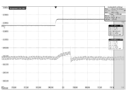
The fabricated chip was tested at a frequency of 1.3 GHz, and the power consumption of the complete synchronizer was 1.4 mW off a 1.2V supply. The chip was found to lie in the FNSP (fast N, slow P) corner. The clock was generated using a three stage inverter ring oscillator, whose frequency was controlled by modulating its supply. No duty cycle correction circuit was included. The tracking of the phase detector was confirmed by deliberately shifiting the clock phase of the transmitter and observing the control voltage of the circuit. Fig. 17 shows the trajectory of the control voltage () when the introduced phase shift in the transmitter does not need a DLL phase increment or decrement. Fig. 18 shows the trajectory of the control voltage when the introduced phase shift in the transmitter needs DLL phase decrements for achieving lock. Once lock is achieved, it was observed that the circuit remains locked over long periods of time, which was tested by monitoring the lock over a period of up to 30 minutes.
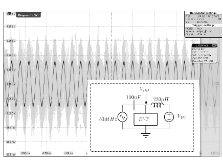
The circuit was also tested with supply voltage fluctuations by adding a sine wave to the supply voltage. Fig. 19 shows the supply voltage as observed on an oscilloscope along with an inset of the circuit used to add a sine wave over the DC supply. Fig. 20 shows the trajectory of the control voltage for the measurement under these conditions.
To confirm scalability of the architecture, the synchronizer was also designed and simulated in TSMC 65 nm CMOS technology, for a data rate of 4 Gbps. The clock division ratio () of 32 was used for deriving the clock for the coarse tuning loop. Rest of the implementation details are identical to the 130 nm implementation. From layout extracted simulations, the power consumption was found to be 1.5 mW drawn from a 1 V supply. The area of the synchronizer is .
Table I compares the performance of previously reported clock synchronizers for repeaterless interconnects with the presented design. As seen from Table I, the proposed synchronizer for repeaterless low swing interconnects is the only one for on-chip interconnects that is adaptive and does not have phase quantization error. Also, to the best of the authors knowledge, this is the only work which discusses clock domain transfer to receiver clock domain for low swing interconnects.
| JSSC’14 [9] | JSSC’05 [16] | JSSC’03 [24] | This work | ||
|---|---|---|---|---|---|
| Process | 65 nm | 110 nm | 110 nm | 130 nm | 65 nm |
| (Measured) | (Simulated) | ||||
| Interconnect type | On-chip | Off-chip | Off-chip | On-Chip | |
| Synchronizer type | Mesochronous | Plesiochronous | Plesiochronous | Mesochronous | |
| Controller type | Digital | Analog | Digital | Coarse digital + fine analog | |
| Adaptive control | No | Yes | Yes | Yes | |
| Clock domain transfer | No | No | No | Yes | |
| Data rate | 3 Gb/s | 10 Gb/s | 10 Gb/s | 1.3 Gb/s | 4 Gb/s |
| Power consumption | 1.08 mW | 220 mW | 129 mW | 1.4 mW | 1.5 mW |
| Supply Voltage | 0.9 V | 1.5 V | 1.2 V | 1.2 V | 1 V |
| Area () | Not reported | 250 1400 | 1600 2600 | 76 80 | 48 50 |
VI Conclusion
This paper presents a clock synchronizing circuit for repeaterless low swing on-chip interconnect. The circuit uses a coarse and a fine correction loop, and permits the lock state of the coarse correction loop to be saved and recalled on subsequent power up, for quick locking. A low latency clock domain transfer then transfers the data to the receiver clock domain. The circuits have been designed and tested in CMOS 130 nm technology. Further, to verify the scalability the circuit, the circuit was also designed and simulated in CMOS 65 nm technology.
Appendix A False edge locking in DLL based CDR loops using the Alexander phase detector
The Alexander phase detector is widely used for measuring the phase difference between data and clock, as required in clock and data recovery circuits [15]. The circuit diagram of the phase detector is shown in Fig. 12. This phase detector samples the data at two points per bit period to make a decision whether the clock is leading or lagging the data. Fig. 21 shows the sampling instants when the clock is late and early.

The UP and DN signals are then derived from the three consecutive samples A, B and C as
| DN | |||
| UP |
This evaluation is performed on the active edge of the clock, and the last three consecutive samples are used. The UP and DN signals are then integrated using a charge pump that controls the clock frequency/phase. The negative feedback loop brings the clock to the center of the eye.
When certain, albeit unlikely, conditions are met the Alexander phase detector can lock to the wrong edge at the center of the eye. This happens when the frequencies of the data and the clock are exactly equal, and the phase of the clock is exactly radians offset from the center of the eye and the data has a 50% activity. Under such conditions the phase detector can lock to the correct edge either by increasing the relative phase by radians, or by reducing the relative phase by radians. Theoretically, the phase detector can take infinite time to choose one solution over the other [25]. Fig. 22 shows the sampling instants for various data transition permutations, when the data and clock have a phase error of radians.

As seen in Fig. 22 (a), if sample C resolves to the same values as A and B no corrective action is performed. If however, C is not equal to A and B, then the phase detector asserts a DN signal. Similarly if this is followed with pattern shown in Fig. 22 (c), only if A resolves unequal to B and C, the phase detector asserts an UP signal. Since the deciding samples are taken within the metastability window of the comparators, these can occur with equal probability nullifying each other. The case in Fig. 22 (b) can also cause an additional case where A and C resolve to a value different from sample at B. This causes the phase detector to assert both UP and DN, which results in no change on the control voltage. However, this case was not observed in simulations, but it is possible in principle. The above conditions can cause the net result such that the phase detector is stuck at the wrong edge.
Generally the randomness in the data and system noise is sufficient to get the phase detector out of this zone. False locking happens when the phase detector’s correct sampling edge is within the meta-stability window of the comparator under the initial conditions. Since the meta-stability window increases after layout, the inertia of staying locked at the false edge is higher when layout extracted circuits are tested. Fig. 23 shows the control voltage () waveform when the phase detector is locked to the wrong edge.
The simulation was performed on pre-layout (schematic) circuit netlist. It is seen that around 0.7 s simulation time, the randomness of the data pushes the clock edge out of the unstable equilibrium zone of the loop and lock to correct edge is achieved in the subsequent 0.6 s.
It may be noted that this phenomenon, in principle, can also occur when the phase detector is used for frequency and phase locking. However, the sweeping of the clock edge across the data eye due to the difference in the clock and data frequency; the required phase detector gain; and the required data sequence to hold the phase detector at the wrong edge; make its probability of occurrence extremely remote.
This problem is not expected to be severely limiting, as noise will eventually bring the system out of the unstable equilibrium. This problem if at all occurs, will only occur the first time around. Once correct lock is achieved, and the state is saved, this false lock will never occur, as the recalled state brings the loop state very close to the correct lock. By using phase detectors that sample the data at more than two times per bit period [26], one can eliminate the probability of the first time occurrence as well.
References
- [1] A. Katoch, H. Veendrick, and E. Seevinck, “High speed current-mode signaling circuits for on-chip wires,” in Proc. of European Solid State Circuits Conf. (ESSCIRC), Sept. 2005, pp. 4138–4141.
- [2] R. Ho, T. Ono, F. Liu, R. Hopkins, A. Chow, J. Schauer, and R. Drost, “High-speed and low-energy capacitively-driven on-chip wires,” in IEEE Int. Solid State Circuits Conf. (ISSCC) Dig. of Tech. Papers, 2007, pp. 412–414.
- [3] Eisse Mensink, Daniel Schinkel, Eric Kiumperink, Ed van Tuiji, and Brain Nauta, “0.28pJ/b 2Gb/s/ch transceiver in 90nm CMOS for 10mm on-chip interconnects,” in IEEE Int. Solid State Circuits Conf. (ISSCC) Dig. of Tech. Papers, Feb. 2007, pp. 414–416.
- [4] Byungsub Kim and Vladimir Stojanovic, “A 4Gb/s/ch 356fJ/b 10mm equalized on-chip interconnect with nonlinear charge-injecting transmit filter and transimpedance receiver in 90nm CMOS,” in IEEE Int. Solid State Circuits Conf. (ISSCC) Dig. of Tech. Papers, 2010, pp. 66–68.
- [5] Byungsub Kim and V. Stojanović and, “An energy-efficient equalized transceiver for RC-dominant channels,” IEEE J. Solid-State Circuits (JSSC), vol. 45, no. 6, pp. 1186–1197, June 2010.
- [6] Jae sun Seo, R. Ho, J. Lexau, M. Dayringer, D. Sylvester, and D. Blaauw, “High-bandwidth and low-energy on-chip signaling with adaptive pre-emphasis in 90nm CMOS,” in IEEE Int. Solid State Circuits Conf. (ISSCC) Dig. of Tech. Papers, Feb. 2010, pp. 138–139.
- [7] K. Naveen, M. Dave, M.S. Baghini, and D.K. Sharma, “A feed-forward equalizer for capacitively coupled on-chip interconnect,” in Proc. 26th IEEE Conf. VLSI Design, 2013, pp. 215–220.
- [8] Shih-Hung Weng, Yulei Zhang, J.F. Buckwalter, and Chung-Kuan Cheng, “Energy efficiency optimization through codesign of the transmitter and receiver in high-speed on-chip interconnects,” IEEE Trans. on VLSI Syst., vol. 22, no. 4, pp. 938–942, April 2014.
- [9] Seung-Hun Lee, Seon-Kyoo Lee, Byungsub Kim, Hong-June Park, and Jae-Yoon Sim, “Current-mode transceiver for silicon interposer channel,” IEEE J. Solid-State Circuits (JSSC), vol. 49, no. 9, pp. 2044–2053, Sept 2014.
- [10] E. Mensink, D. Schinkel, E.A.M. Klumperink, E. van Tuijl, and B. Nauta, “Power Efficient Gigabit Communication Over Capacitively Driven RC-limited On-Chip Interconnects,” IEEE J. Solid-State Circuits (JSSC), vol. 45, no. 2, pp. 447–457, Feb. 2010.
- [11] Seon-Kyoo Lee, Seung-Hun Lee, D. Sylvester, D. Blaauw, and Jae-Yoon Sim, “A 95fJ/b current-mode transceiver for 10mm on-chip interconnect,” in IEEE Int. Solid State Circuits Conf. (ISSCC) Dig. of Tech. Papers, Feb 2013, pp. 262–263.
- [12] R.T. Chang, N. Talwalkar, C.P. Yue, and S.S. Wong, “Near speed-of-light signaling over on-chip electrical interconnects,” IEEE J. Solid-State Circuits (JSSC), vol. 38, no. 5, pp. 834 – 838, May 2003.
- [13] Ruibing Lu, Guoan Zhong, Cheng-Kok Koh, and Kai-Yuan Chao, “Flip-flop and repeater insertion for early interconnect planning,” in Proc. IEEE Design Autom. Test Eur. (DATE) Conf., 2002, pp. 690–695.
- [14] M. Ghoneima, Y. Ismail, M. Khellah, and V. De, “SSMCB: Low-Power Variation-Tolerant Source-Synchronous Multicycle Bus,” IEEE Trans. Circuits Syst. I (TCAS-I), vol. 56, no. 2, pp. 384–394, Feb 2009.
- [15] B. Razavi, “Challenges in the design high-speed clock and data recovery circuits,” IEEE Communications Magazine, vol. 40, no. 8, pp. 94–101, 2002.
- [16] R. Kreienkamp, Ulrich Langmann, C. Zimmermann, T. Aoyama, and H. Siedhoff, “A 10Gb/s CMOS clock and data recovery circuit with an analog phase interpolator,” IEEE J. Solid-State Circuits (JSSC), vol. 40, no. 3, pp. 736–743, March 2005.
- [17] Yeon-Jae Jung, Seung-Wook Lee, Daeyun Shim, Wonchan Kim, Changhyun Kim, and Soo-In Cho, “A dual-loop delay-locked loop using multiple voltage-controlled delay lines,” IEEE J. Solid-State Circuits (JSSC), vol. 36, no. 5, pp. 784–791, May 2001.
- [18] S. Sidiropoulos and M.A. Horowitz, “A semidigital dual delay-locked loop,” IEEE J. Solid-State Circuits (JSSC), vol. 32, no. 11, pp. 1683–1692, Nov. 1997.
- [19] John W. Poulton William J. Dally, Digital Systems Engineering, Cambridge University Press, 1998.
- [20] R Jacob Baker, Chapter 27 : CMOS Circuit Design, Layout, and Simulation, Third Edition, Wiley-IEEE Press, 2010.
- [21] B. Nikolic, Vojin G. Oklobdzija, V. Stojanovic, Wenyan Jia, James Kar-Shing Chiu, and M. Ming-Tak Leung, “Improved sense-amplifier-based flip-flop: design and measurements,” IEEE J. Solid-State Circuits (JSSC), vol. 35, no. 6, pp. 876–884, June 2000.
- [22] M.G. Johnson and E.L. Hudson, “A variable delay line PLL for CPU-coprocessor synchronization,” IEEE J. Solid-State Circuits (JSSC), vol. 23, no. 5, pp. 1218–1223, Oct. 1988.
- [23] H. Farkhani, M. Meymandi-Nejad, and M. Sachdev, “A fully digital ADC using a new delay element with enhanced linearity,” in Proc. IEEE Int. Symp. Circuits and Systems (ISCAS), May 2008, pp. 2406–2409.
- [24] H. Takauchi, Hirotaka Tamura, S. Matsubara, M. Kibune, Y. Doi, T. Chiba, H. Anbutsu, H. Yamaguchi, T. Mori, Motomu Takatsu, K. Gotoh, T. Sakai, and T. Yamamura, “A CMOS multichannel 10Gb/s transceiver,” IEEE J. Solid-State Circuits (JSSC), vol. 38, no. 12, pp. 2094–2100, Dec. 2003.
- [25] Leslie Lamport, “Buridan’s principle,” Foundations of Physics, vol. 42, no. 8, pp. 1056–1066, 2012.
- [26] Nikola Nedovic, N. Tzartzanis, Hirotaka Tamura, F.M. Rotella, M. Wiklund, Y. Mizutani, Y. Okaniwa, T. Kuroda, J. Ogawa, and W.W. Walker, “A 40-44 Gb/s 3x oversampling CMOS CDR/1:16 DEMUX,” IEEE J. Solid-State Circuits (JSSC), vol. 42, no. 12, pp. 2726–2735, Dec 2007.
![[Uncaptioned image]](/html/1510.04241/assets/x7.png) |
Naveen Kadayinti is a research scholar at the Indian Institute of Technology Bombay, and is currently working towards his thesis on “High speed interconnects”. His research interests include wired and wireless communication circuits and mixed signal SoC design and test. |
![[Uncaptioned image]](/html/1510.04241/assets/x8.png) |
Maryam Shojaei Baghini (M’00 - SM’09) received the M.S. and Ph.D. degrees in electrical engineering from Sharif University of Technology, Tehran, in 1991 and 1999, respectively. She has worked for more than 2 years in industry on the design of analog ICs. In 2001, she joined Department of Electrical Engineering, IIT-Bombay, as a Postdoctoral Fellow, where she is currently a Professor. She is the author/coauthor of 143 international journal and conference papers, the inventor/coinventor of 6 granted US patents, 1 granted Indian patent and 25 more filed patent applications. Her current research interests include high-speed links for on-chip and off-chip data communication, high-performance low-energy analog/mixed-signal/RF IC design and test for various applications including healthcare and sensor networks, device-circuit co-design in emerging technologies and energy harvesting circuits and systems. Dr. Shojaei serves in the Technical Program Committee of several IEEE conferences, including IEEE International Conference on VLSI Design, and Asia Symposium on Quality Electronic Design. She was a TPC member of IEEE-ASSC from 2009 to 2014. Dr. Shojaei is joint recipient of 11 awards and a senior member of IEEE. |
![[Uncaptioned image]](/html/1510.04241/assets/x9.png) |
Dinesh Sharma
obtained his Ph.D. from the Tata Institute of Fundamental
Research, Mumbai. He has worked at TIFR and IITB at Mumbai, at LETI at Grenoble in
France and at the Microelectronics Center of North Carolina in the U.S.A. on MOS
technology, devices and mixed mode circuit design. He has been at the EE deptt. of IIT
Bombay since 1991, where he is currently a Professor. His current interests include mixed
signal design, interconnect technology and the impact of technology on design styles.
He is a senior member of IEEE, a fellow of IETE and has served on the editorial board of ”Pramana”, published by the Indian Academy of Science. |