Ultrafast Response of Monolayer Molybdenum Disulfide Photodetectors
Abstract
The strong light emission and absorption exhibited by single atomic layer transitional metal dichalcogenides in the visible to near-infrared wavelength range makes them attractive for optoelectronic applications. In this work, using two-pulse photovoltage correlation technique, we show that monolayer molybdenum disulfide photodetector can have intrinsic response times as short as 3 ps implying photodetection bandwidths as wide as 300 GHz. The fast photodetector response is a result of the short electron-hole and exciton lifetimes in this material. Recombination of photoexcited carriers in most two-dimensional metal dichalcogenides is dominated by non-radiative processes, most notable among which is Auger scattering. The fast response time, and the ease of fabrication of these devices, make them interesting for low-cost ultrafast optical communication links.

Two dimensional (2D) transition metal dichalcogenides (TMDs) have emerged as interesting materials for low-cost opto-electronic devices, including photodetectors, light-emitting diodes, and, more recently, lasers Mak10 ; Splendiani10 ; Wang12 ; Mak13 ; Lopez13 ; Ross14 ; Hua12 ; Steiner13 ; Baugher14 ; Changjian14 ; Sanfeng15 . In the case of photodetectors, the response time and the quantum efficiency are two important figures of merit. The intrinsic response time of TMD photodetectors and the ultimate limits on the speed of operation are unknown. The reported quantum efficiencies of TMD materials and devices are typically in the .0001-0.01 range Lopez13 ; Hua12 ; Wang15 ; Steiner13 ; Ross14 ; Grossman14 ; Thomas14 ; Baugher14 ; Thomas14b , indicating that most of the electrically injected or optically generated electrons and holes recombine nonradiatively. Understanding the nonradiative carrier recombination mechanisms, as well as the associated time scales, is therefore important. Previously, ultrafast optical/THz pump-probe as well as ultrafast photoluminescence techniques have been used, by the authors and others, to study the ultrafast carrier dynamics in metal dichalcogenides and in molybdenum disulfide (MoS2) in particular Wang15 ; Huang13 ; WangR12 ; Choi13 ; Sun14 ; Lagarde14 ; Schuller11 ; Docherty14 . In these measurements, free-carrier recombination dynamics, exciton formation and recombination dynamics, refractive index changes, optical/THz intraband and interband conductivity changes, as well as the dynamics associated with carriers trapped in optically active midgap defects are all expected to play a role to varying degrees and, consequently, the results have been difficult to interpret and reconcile.
In this letter, we present experimental results on ultrafast two-pulse photovoltage correlation (TPPC) measurements on monolayer MoS2 metal-semiconductor photodetectors. In TPPC measurements, a photodetector is excited with two identical optical pulses separated by a time delay and the integrated detector photoresponse (either photovoltage or photocurrent response) is recorded as a function of the time delay. TPPC thus uses the photodetector to perform an optical correlation measurement. The nonlinearity of the photoresponse with respect to the optical pulse energy enables one to determine ultrafast intrinsic temporal response of the detector with sub-picosecond resolution Ulrich11 ; Holleitner11 ; Holleitner12 ; McEuen13 ; Sun12 . Our measurements show that the photovoltage is suppressed when the two optical pulses arrive together indicating a saturation of the photoresponse. As the time delay between the two pulses is increased from zero, the photovoltage recovers, and the recovery, as a function of the time delay, exhibits two distinct timescales: (i) a fast timescale of the order of 3 to 5 ps, and (ii) a slow timescale of around 80 to 110 ps. These two timescales are found to be largely independent of the temperature, exhibits only a mild dependence on the pump fluence, and varies a little from sample to sample. Between 50-75 of the photovoltage correlation response recovers on the fast timescale implying that ultrafast TMD photodetectors with (8 dB) current modulation bandwidths in the 200-300 GHz range are possible. The fast response speed is a result of the short lifetime of the photoexcited carriers. Since TPPC measures the photovoltage (or photocurrent), this technique is sensitive only to the total photoexcited carrier population, including both bound (excitons) and free carriers, that contributes to the photoresponse. TPPC therefore also offers important and unique insights into the carrier recombination dynamics. The temperature and pump fluence dependence of our TPPC results are consistent with defect-assisted recombination as being the dominant mechanism, in which the the photoexcited electrons and holes, both free and bound (excitons), are captured by defects via Auger scattering Wang15b . Strong Coulomb interactions in 2D TMDs, including the correlations in the positions of free and bound electrons and holes arising from the attractive interactions, result in large carrier capture rates by defects via Auger scattering Wang15b . Our results underscore the trade-off between speed and quantum efficiency in TMD photodetectors.
I Results
I.1 Two-Pulse Photovoltage Correlation Technique

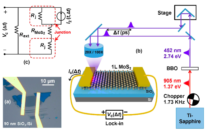
Microscope image of a monolayer metal-MoS2 photodetector is shown in Figure 2(a), and the schematic in Figure 2(b) depicts the setup for a two-pulse photocurrent/photovoltage correlation (TPPC) experiment. A 80 fs, 905 nm (1.37 eV) center wavelength, optical pulse from a 83 MHz repetition rate Ti-Sapphire laser is frequency doubled to 452 nm (2.74 eV, 150 fs) by a beta-BaB2O4 crystal, then mechanically chopped at 1.73 KHz, and then split into two pulses by a 50/50 beam splitter. The time delay between these two pulses is controlled by a linear translation stage. The resulting voltage across the photodetector is measured as a function of the time delay between the pulses using a lock-in amplifier with a 10 M input resistance. In experiments, the maximum photoresponse was obtained when the light was focused on the sample near one of the metal contacts of the device, and the photoresponse decayed rapidly as the center of the focus spot was moved more than half a micron away from the metal contact. The direction of the DC photocurrent, and the resulting sign of the measured DC photovoltage are shown in Figure 2(b), and were determined without using the lock-in. Photovoltage was always positive at the contact near which the light was focused. Figure 2(c) shows a low-frequency circuit model of the device and the measurement. The circuit model shown can be derived from a high-frequency circuit model(Supplementary Figure 2 and Note 3). If the time-dependent short circuit current response of the illuminated junction to a single optical pulse is , and to two optical pulses separated by time is , and the external resistance is much larger than the total device resistance, then the measured DC voltage is approximately equal to , where is the pulse repetition period, is the resistance of the metal-MoS2 junction, and the time integral is over one complete period. As the time delay becomes much longer than the duration of , one expects to approach .
I.2 Experimental Results
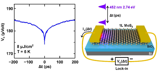
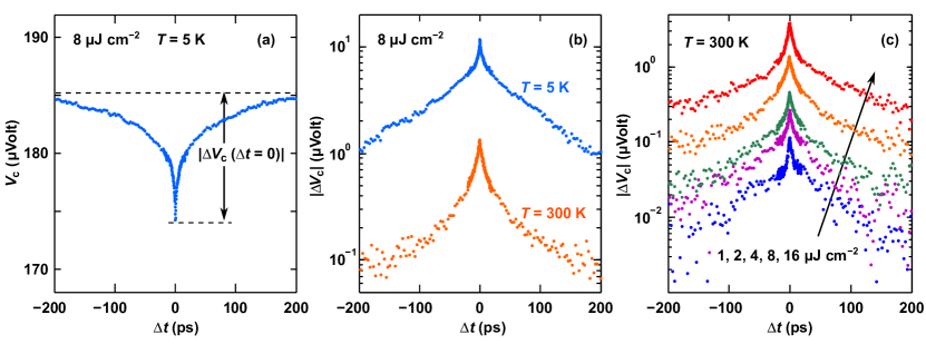
3(a) shows the measured two-pulse photovoltage correlation signal plotted as a function of the time delay between the pulses. The substrate temperature is 5K, the gate bias is 0 V, and the pump fluence is 8 J cm-2. is minimum when the two pulses completely overlap in time (i.e. when ). This implies, not surprisingly, that the photovoltage response of the detector to an optical pulse is a sublinear function of the optical pulse energy. As increases from zero, also increases from its minimum value at . As becomes much longer than the duration of the response transient of the detector to an optical pulse, approaches a constant value. The timescales over which goes to the constant value are related to the timescales associated with the response transient of the detector to an optical pulse. These timescales are better observed in the measured data if the magnitude of , defined as , is plotted on a log scale, as shown in Figure 3(b). The plot in Figure 3(b) shows two distinct timescales: (i) a fast timescale of 4.3 ps, and (ii) a slow timescale of 105 ps. In different devices, the fast timescales were found to be in the 3-5 ps range, and the slow timescales were in the 90-110 ps range. The fast timescales imply (8 dB) current modulation bandwidths wider than 300 GHz.
Measurements were performed at different temperatures and using different pump pulse fluences in order to understand the mechanisms behind the photoresponse and the associated dynamics. Figure 3(b) shows plotted for two different extreme temperatures: = 5K and = 300K. Gate bias is 0 V. The pump fluence is 8 J cm-2. Two distinct timescales are observed at both temperatures and these timescales are largely independent of the temperature. Measurements performed at intermediate temperatures provided the same results. was found to be larger at smaller temperatures. We attribute this to the increase in the metal-semiconductor junction resistance at lower temperatures. Figure 3(c) shows plotted for different values of the pump pulse fluence. The pump pulse fluence was varied from 1 J cm-2 to 16 J cm-2. Higher values of the pump fluence were not used in order to avoid optical damage to the sample Wang15 . = 300K and gate bias is 0 V. Figure 3(c) shows that the same two timescales are observed for all values of the pump fluence and these timescales are not very sensitive to the pump fluence. The observed timescales also did not change in any significant way under a positive or a negative gate bias (Supplementary Figure 3, Figure 4 and Note 4). The internal and external detector quantum efficiencies were estimated from the measured values of and the junction resistance to be in the 0.008-0.016 and 0.001-0.002 ranges, respectively.
The two different timescales observed in our two-pulse photovoltage correlation experiments match well with the two different timescales observed previously in ultrafast optical/THz pump-probe studies of carrier dynamics as well as in ultrafast photoluminescence studies of MoS2 monolayers Wang15 ; Docherty14 . It is therefore intriguing if the model for defect-assisted carrier recombination reported previously by the authors Wang15 ; Wang15b for explaining the ultrafast carrier dynamics in MoS2 monolayers can be used to obtain photovoltage correlations that are in good agreement with the experimental results reported in this letter. We show below that this is indeed the case.

I.3 Ultrafast Photoresponse of the Metal-MoS2 Junction
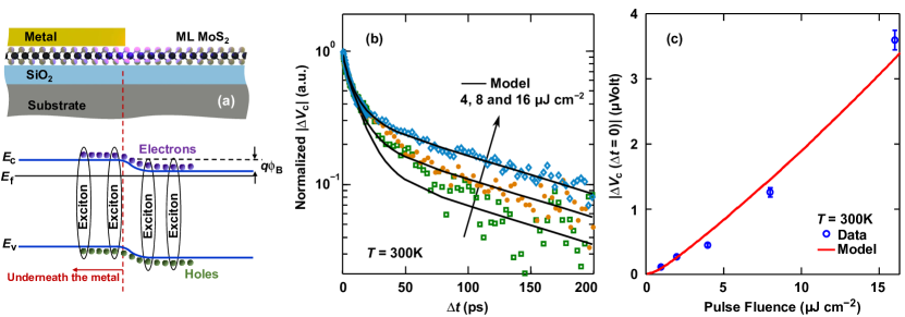
Understanding the ultrafast photoresponse of the detector, and in particular the short circuit current response , is important for interpreting the experimental results. Figure 4(a) depicts the band diagram of the metal-MoS2 junction (plotted in the plane of the MoS2 layer) after photoexcitation with an optical pulse. Given the Schottky barrier height of 100-300 meV Steiner13 , the width of the MoS2 region near the metal with a non-zero lateral electric field is estimated to be to 100-300 nm Shik89 . As a result of light diffraction from the edge of the metal contact, light scattering from the substrate, and plasmonic guidance, a portion of the MoS2 layer of length equal to a few hundred nanometers is photoexcited even underneath the metal (Supplementary Figure 1 and Note 1). The photoresponse of graphene photodetectors has been explained in terms of contributions from photovoltaic and photothermoelectric contributions Ulrich11 ; Holleitner11 ; Holleitner12 ; McEuen13 ; Sun12 ; Koppens15 . In our MoS2 samples, the carrier mobilities and diffusivities are 2-3 orders of magnitude smaller than in graphene and the time period in which most of the photoexcited carriers recombine and/or are captured by defects is in the few picoseconds range Wang15 ; Wang15b ; Docherty14 ; Lagarde14 ; Schuller11 . Assuming similar mobilities and diffusivities of electrons and holes in MoS2, the photoexcited carriers, both free and bound (excitons), move, either by drift in the junction lateral electric field or by diffusion, less than 10 nm in 5 ps before they recombine and/or are captured by defects. The photoexcited carrier distributions therefore do not change significantly in space during their lifetime. Separation of electrons and holes either by the junction lateral electric field or at the metal-MoS2 interface will contribute to the integral (the measured dependence of the photoresponse on the junction electric field and the gate voltage is discussed in the Supplementary Figure 3, Figure 4 and Note 4. We assume that the integral is approximately proportional to the integral (Supplementary Note 2). Here, and are the time-dependent photoexcited electron and hole densities in the junction, including carriers both free and bound (excitons). This assumption, although simple, allows one to relate the measured photoresponse to the carrier dynamics and, as shown below, the results thus obtained are in excellent agreement with the experiments. We expect that on much longer timescales, when the photoexcited carriers have recombined or been captured, the photoresponse is entirely thermoelectric in nature, as is the case in metal-graphene photodetectors Ulrich11 ; Holleitner12 ; McEuen13 ; Sun12 ; Koppens15 . But in this letter we focus on the dynamics occurring on only short timescales.
I.4 Carrier Capture/Recombination Model and Comparison with Data
It is known that most of the photoexcited carriers in monolayer MoS2 recombine non-radiatively Wang15 ; Wang15b ; Thomas14b . The temperature independence as well as the sample dependence of the recombination rates in previously reported works suggested that free and bound (excitons) carriers recombine via capture by defects through Auger scattering Wang15 ; Wang15b . Monolayer MoS2 can have several different kinds of defects, including grain boundaries, line defects, interstitials, dislocations and vacancies Sofo04 ; Komsa12 ; Seifert13 ; Zhou13 ; Kim14 ; Guinea14 ; Robertson13 . The strong electron and hole Coulomb interaction in monolayer TMDs makes defect capture via Auger scattering very effective Wang15b . The time constants observed in this work in the photovoltage correlations are also temperature independent (see Figure 3(b)) and also match well with the time constants observed previously in optical/THz pump-probe and photoluminescence measurements Wang15 ; Docherty14 . We therefore use the model for carrier capture by defects via Auger scattering in MoS2 presented by Wang et al. Wang15 ; Wang15b to model our TPPC experimental results (Supplementary Figure 5 and Note 5). The model assumes carrier capture by two different defect levels, one fast and one slow Wang15 . The essential dynamics captured by the model, and their relationships to the experimental observations, are as follows Wang15 . After photoexcitation, electrons and holes thermalize and lose most of their energy on a timescale much shorter than our experimental resolution (0.5-1.0 ps) and, therefore, thermalization is assumed to happen instantly in our model Kaas14 . Most of the photoexcited holes (both free and bound), followed by most of the electrons, are captured by the fast defects within the first few picoseconds after photoexcitation. During the same period, a small fraction of the holes is also captured by the slow defects. This rapid capture of the photoexcited electrons and holes is responsible for the fast time constant observed in our photovoltage correlation experiments. The remaining photoexcited electrons are captured by the slow defects on a timescale of 65-80 ps and this slow capture of electrons is responsible for the slow time constant observed in our photovoltage correlation experiments. We should point out here that the two time constants observed in the photovoltage correlation signal are always slightly longer than the corresponding two time constants exhibited by the carrier densities in direct optical pump-probe and measurements Wang15 , as is to be expected in the case of correlation measurements. Finally, the superlinear dependence of the carrier capture rates on the photoexcited carrier densities in the model, and therefore on the optical pulse energy, results in the experimentally observed negative value of the photovoltage correlation signal at zero time delay. The values of the fitting parameters used in the theoretical model to fit the experimental data are given in the Supplementary Table 1 and are almost identical to the values extracted previously from direct optical pump-probe measurements of the carrier dynamics in monolayer MoS2 Wang15 .

The comparison between the data and the model are shown in Figure 4(b) which plots the measured and computed photovoltage correlation as a function of the time delay for different pump fluence values: 4, 8, and 16 J cm-2. All curves are normalized to a maximum value of unity (since the model gives the photovoltage correlation signal up to a multiplicative constant). The model not only reproduces the very different timescales observed in measurements, it achieves a very good agreement with the data over the entire range of the pump fluence values used in our experiments for the same values of the parameters (Supplementary Table 1). Figure 4(c) shows the scaling of the measured and computed values of with the pump pulse fluence. Again, a very good agreement is observed between the model and the data.
II Discussion
Our results reveal the fast response time and the wide bandwidth of metal-MoS2 photodetectors and show that these detectors can be used for ultrafast applications. Our results also shed light on the carrier recombination mechanisms and the associated timescales. Although we focused mainly on the carrier dynamics in this paper, the device intrinsic resistances and capacitances are not expected to fundamentally limit the device speed because of the rather small capacitances associated with the lateral metal-semiconductor junctions (Supplementary Note 3). An obstacle to using TMDs in practical light emission and detection applications is the small values of the reported quantum efficiencies in these materials Lopez13 ; Hua12 ; Wang15 ; Steiner13 ; Ross14 ; Grossman14 ; Thomas14 ; Baugher14 ; Thomas14b . In photodetectors, the response speed and the quantum efficiency are often inversely related Donati99 . In most semiconductor photovoltaic detectors with large carrier mobilities and long recombination times (e.g. group III-V semiconductor photodetectors Donati99 ), the transit time of the photogenerated carriers through the junction depletion region determines the detector bandwidth Donati99 . Given the relatively small carrier mobilities and diffusivities in MoS2, the fast carrier recombination times determine the speed in our metal-MoS2 detectors. The price paid for the the fast response time is the small internal quantum efficiency: most of the photogenerated carriers recombine before they make it out into the circuit. The best reported carrier mobilities in monolayer MoS2 are an order of magnitude larger than in our devices and, therefore, metal-MoS2 photodetectors with internal quantum efficiencies around 0.1 (approximately an order of magnitude larger than of our devices) are possible without sacrificing the wide bandwidth. Density of defects, which contribute to carrier trapping and recombination, is also a parameter that can be potentially controlled in 2D TMD optoelectronic devices to meet the requirements for ultrafast or high quantum efficiency applications. In addition, vertical heterostructures of 2D TMD materials can also be used to circumvent the transport bottleneck in high speed applications Koppens15b .
III Methods
III.1 Device Fabrication and Characterization
Monolayer MoS2 samples were mechanically exfoliated from bulk MoS2 crystal (obtained from 2D Semiconductors Inc.) and transferred onto highly n-doped Si substrates with 90 nm thermal oxide. Monolayer sample thickness was confirmed by Raman and reflection spectroscopies Ryu10 . Au metal contacts (with a very thin Cr adhesion layer) were patterned and deposited onto the samples using electron-beam lithography. The doped Si substrate acted as the back gate. Microscope image of a 1010 m2 area device is shown in Figure 2(a). Carrier densities and mobilities in the devices were determined using electrical transport measurements on devices of different dimensions. The devices were found to be n-doped with electron densities around - cm-2 (under zero gate bias). The intrinsic doping was attributed to impurities and defect levels Steiner13 . The electron mobility in the devices was found to be in the cm2 V-1s-1 range at 5K. The zero gate bias device resistance was typically less than 1 M at all temperatures for a 1010 m2 area device. While the device resistance decreased under a positive gate bias, no signature of hole conduction was observed even when a large negative gate bias was applied indicating that the Fermi level in the MoS2 layer was likely pinned at defect levels within the bandgap under a negative gate bias. The devices were mounted in a helium-flow cryostat and the temperature was varied between 5K and 300K during measurements. The zero gate bias device resistance was found to be a function of the temperature and decreased almost linearly with the temperature from 1 M at 5K to values 5-7 times smaller at 300K. The total device resistance was dominated by the metal Schottky contacts to the device. For example, at 5K the resistance contributed by the 1010 m2 area MoS2 strip is estimated to be in the 0.10-0.20 M range (from the measured mobility values), which is approximately only one-tenth to one-fifth of the total device resistance. The reported Schottky barrier heights between similarly n-doped monolayer MoS2 and Au/Cr contacts are in the 100-300 meV range Steiner13 . Depending on how strongly the Fermi level gets pinned at the defect levels in the bandgap, the lateral potential drop in the MoS2 layer at the metal-MoS2 interface (depicted in Figure 4(a)) could be equal to or smaller than the Schottky barrier height.
III.2 TPPC Experiment Setup
In the TPPC measurements, the two 452 nm optical pulses were cross-polarized to minimize interference and focused onto the device using a 20X or a 100X microscope objective resulting in a minimum focus spot size of around 0.75 m. Optical absorption in monolayer MoS2 layers was characterized using a confocal microscope based relection/transmission setup Wang15 and yielded around 11%-12% absorption (single-pass) in monolayer MoS2 on oxide at 452 nm (pump pulse wavelength). Measurement of the photovoltage using a high input impedance voltage amplifier (Lock-in in our case) was found to give a much better signal-to-noise ratio than the measurement of the photocurrent directly using a low input impedance transimpedance amplifier.
Acknowledgments
The authors would like to acknowledge helpful discussions with Jared H. Strait, Michael G. Spencer, and Paul L. McEuen, and support from CCMR under NSF grant number DMR-1120296, AFOSR-MURI under grant number FA9550-09-1-0705, ONR under grant number N00014-12-1-0072, and the Cornell Center for Nanoscale Systems funded by NSF.
Author contributions
H. W. performed the experiments, modelling, and simulation. C.Z and W.M.C fabricated the devices. S.T. and F.R initiated and supervised the work.
Additional information
Correspondence and requests for materials should be addressed to H.W and F.R.
References
- (1)
- (2)