Photoluminescence from voids created by femtosecond laser pulses inside cubic-BN
Abstract
Photoluminescence (PL) from femtosecond laser modified regions inside cubic-boron nitride (c-BN) was measured under UV and visible light excitation. Bright PL at the red spectral range was observed, with a typical excited state lifetime of ns. Sharp emission lines are consistent with PL of intrinsic vibronic defects linked to the nitrogen vacancy formation (via Frenkel pair) observed earlier in high energy electron irradiated and ion-implanted c-BN. These, formerly known as the radiation centers, RC1, RC2, and RC3 have been identified at the locus of the voids formed by single fs-laser pulse. The method is promising to engineer color centers in c-BN for photonic applications.
pacs:
78.55.-m; 78.47.jd; 79.20.Eb; 77.84.BwInvestigation of high pressure and temperature phases of different materials are spanning from the fundamental research Gleason et al. (2015); Fletcher et al. (2015); Xu, Shankland, and Poe (2000) as a recently demonstrated metallic bonding in hydrogen Knudson et al. (2015) to developing new pathways of material synthesis for future practical use McMillan (2002). Structural modifications inside transparent materials can be controlled down to sub-wavelength resolution Shimotsuma et al. (2003); Hnatovsky et al. (2011) by direct laser write and opens possibility to create micro-optical Beresna et al. (2011) and mechanical Bellouard, Said, and Bado (2005) elements, waveguides Burghoff, Nolte, and Tünnermann (2007); Ams et al. (2009); Della Valle, Osellame, and Laporta (2009), to render a chemically resistant material wet-bath etchable for microfluidic applications Marcinkevicius et al. (2001). Of a particular interest are wide band gap materials, such as Cubic BN (c-BN) with a bulk modulus of GPa and a wide bandgap of 6.5 eV. It is made by the diamond anvil cell (DAC) or belt-type high pressure compression of a hexagonal phase h-BN Taniguchi et al. (2002).
Optical properties of boron nitrides are attracting an increasing interest due to their ability to host optically stable single photon emitters at room temperature Aharonovich and Neu (2014) and their hyperbolic properties. To this extent, sub-bandgap excitation of controllably formed and patterned defects in c-BN is strongly anticipated. Moreover, theoretical modeling predicts an analog of the nitrogen-vacancy NV- centers known in diamond for the B-vacancy oxygen pair in c-BN Abtew et al. (2014), which is yet to be confirmed experimentally. The stacking fault energy mJ.m-2 in c-BN is comparable to that in diamond Nistor et al. (1999) and a similar defect formation is expected.

Here, we employ a femtosecond (fs)-laser irradiation technique Kudrius, Šlekys, and Juodkazis (2010); Watanabe et al. (1999) to create optically active color centers in c-BN. Using confocal microscopy and time resolved measurements, we show that the formed voids are extremely bright PL sources and originates from the N-vacancy related radiation center RC-defects Shishonok and Steeds (2004) observed earlier in c-BN only by high energy particle or ionising radiation exposure Erasmus and Comins (2004).
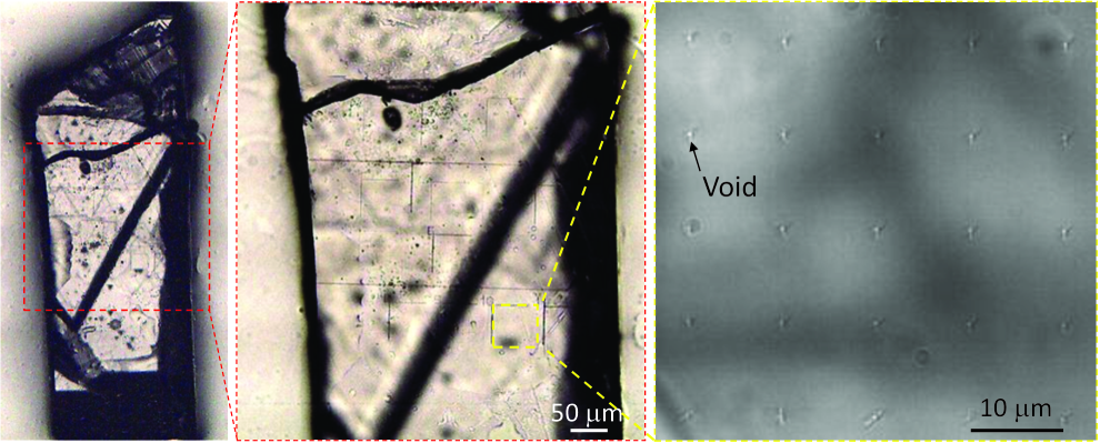
Samples of c-BN were grown on a belt-type high pressure equipment Taniguchi et al. (2002) and were used for experiments of void formation by single femtosecond (fs-)laser pulses tens of micrometers below the surface (Fig. 1).

Laser pulses of fs duration at fundamental nm and second harmonic 515 nm wavelengths were focused at a m depth below the surface of a facet plane inside c-BN crystals (Fig. 1). Tight focusing with numerical aperture was implemented to form arrays of damage sites recorded at different pulse energies at a single pulse conditions. Separation between irradiation spots was 10 m to eliminate a cross talk for void-formation and optical characterization. For comparison, dense array of ablation patterns were fabricated with 800 nm/150 fs pulses focused with on the surface of c-BN. Judgement of the void presence at the center of irradiated spot inside c-BN was made by a sharp optical contrast change which was identical to the void formation in crystalline sapphire, quartz and glasses of different refractive indices Juodkazis et al. (2006a); Hashimoto, Juodkazis, and Misawa (2006); focused ion milling will be implemented next to reveal an internal structure of the void as it was made for voids at the Si-SiO2 interface Rapp et al. (2015).
Photoluminescence and its transients were measured under laser diode 405 nm/30 ps or 510 nm/100 ps (PiLAS; advanced Laser Diode systems) excitation using objective lens and a single photon counting avalanche photo diode (SPCM-AQRH-14) as a detector. A spectral window of PL collection was filter selected at 620-650 nm. A piezo-scanner was implemented to record a PL map around the void-structures. PL spectra were recorded by a spectrometer (Princeton Instruments). Raman spectra were acquired with an InVia Streamline microscope (Renishaw, UK) under 785 nm excitation and focusing.
Strong optical contrast changes were observed at the focus of tightly focused fs-laser pulse in c-BN at the threshold values of nJ ( nm) and 80 nJ (1030 nm) estimated. Due to high refractive index of Satta, Palummo, and Onida (2001) at the used wavelength, a spherical aberration defines the focal volume which became slightly larger Marcinkevicius et al. (2003) as compared with the diffraction-limited focal size of diameter . At such tight focusing, a self focusing is avoided since 10 nJ pulse corresponds to only 43 kW/pulse power but reach 7.1 TW/cm2 irradiance for nm. These are direct write conditions with irradiance of TW/cm2 when voids are formed in different transparent materials under equivalent focusing Juodkazis et al. (2006a); Hashimoto, Juodkazis, and Misawa (2006). The voids are of sub-wavelength nm in diameters Juodkazis et al. (2006a); Hashimoto, Juodkazis, and Misawa (2006) and their actual size has to be measured using focused ion beam cross sections. Micro-cracks comparable in size with the central void-structure were observed in c-BN when the void-structure was created by a single focused fs-laser pulse (Fig. 1). These strongly modified regions were subject of further examination using PL (Fig. 3).

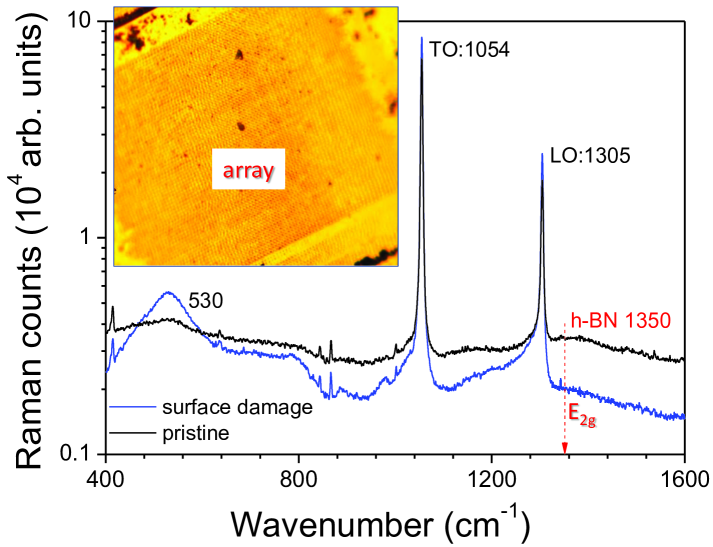
When void is formed in c-BN it could be expected that relaxation into a less dense phase of h-BN or into an amorphous phase occurs. To test this conjecture an ablation on the surface was carried out and Raman scattering measured. Characteristic transversal and longitudinal optical phonon modes TO and LO, respectively, were observed with small broadening at the high-energy side of the modes. Back-scattered Raman signal excited by 785 nm irradiation was collected with a lens averaging response from area with several ablation sites made by single pulses. Wide peak at 520 cm-1 (65.7 meV) was the strongest modification observed from surface ablated regions made by 800 nm/150 fs pulses. Presence of a lower density h-BN was not confirmed from ablated regions which would be recognisable by its 1350 cm-1 E2g mode Reich et al. (2005). Widening of the Raman peak at the LO and TO modes could be related to disordering at the void region, however there is no obvious shift to smaller wavenumbers which takes place for nano-crystallites of c-BN Werninghaus et al. (1997).

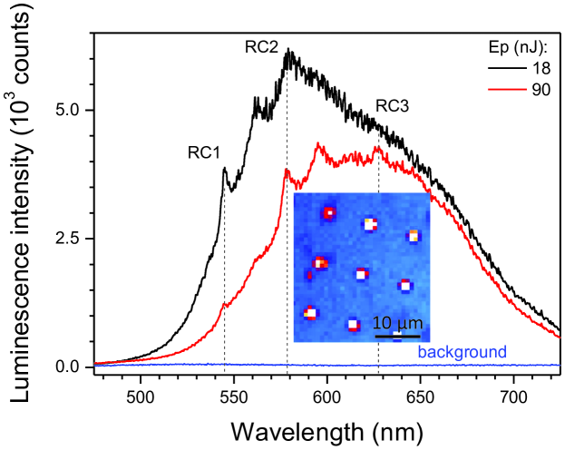
Confocal microscopy with 405 nm excitation source was employed to characterize the fabricated voids-structures in c-BN. Photoluminescence of nitrogen is well studied in atmospheric discharge experiments and lightning observations with lines at deep-UV and at 455, 556, 577 nm identified as atomic neutral nitrogen N Uman (1984). Under 405 nm illumination, PL from the void regions has recognizable features within similar spectral range (Fig. 3). Molecular N2 PL which occurs in 300-400 nm window was out of the range of observation in this first experiment. The confocal map is shown in inset of Fig. 3. The bright spots correspond to the location of the voids.
The observed PL features are matching perfectly the intrinsic vibronic defects RC1,2,3 reported in c-BN irradiated by high energy 1.9 MeV electrons Shishonok and Steeds (2004); Erasmus and Comins (2004). It is noteworthy that PL was measured at room temperature and no post-irradiation annealing was required as it is usually the case after ion implantation. The intrinsic Frenkel pair defects due to the N-vacancy formation earlier observed in cathodo-luminescence (CL) and identified as RC1 with zero phonon line of (2.27 eV, 546.2 nm), RC2 (2.15 eV, 576.7 nm) and RC3 (1.99 eV, 623.1 nm) Shishonok and Steeds (2004); Erasmus and Comins (2004) were found matching very well the defect PL we observed from the voids made by fs-laser pulses (see, Table 1). Deterministic fabrication of these color centesr is demonstrated here for the first time using ultra short light pulses.
| Defect | CL [nm] | PL [nm] |
|---|---|---|
| Radiation | 4.5 MeV electrons Erasmus and Comins (2004) | fs-laser pulse |
| Center (RC) | (this study) | |
| RC1 | 546.2 | |
| RC2 | 576.7 | |
| RC3 | 623.1 |
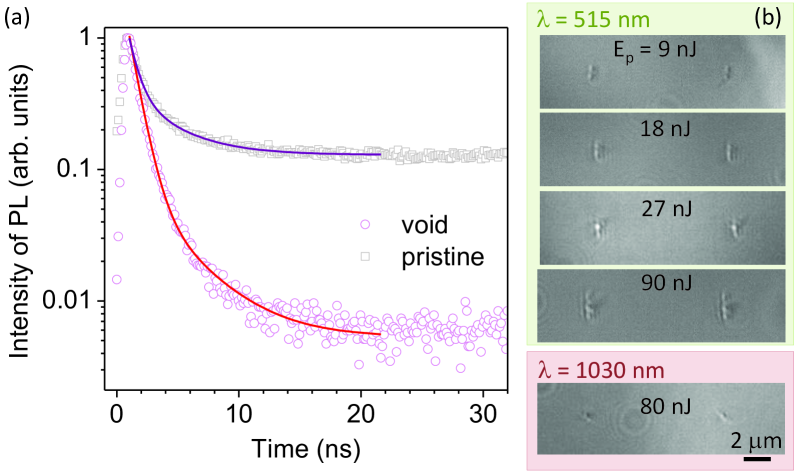
The PL excited at 510 nm/100 ps illumination showed close to a single exponential decay with time constant of 3.7 ns (Fig. 4(a)), while under the 405 nm/30 ps excitation the decay was also similar 4 ns (not shown). Long stretched exponential decay is usually indicative of a recombination of the electrons and holes trapped on defects which are distributed in energy and separated spatially by varying distances. Very long multi-exponential decays were observed in silica glass with nano-gratings formed by fs-laser irradiation as measured by a time-domain method de Jong et al. (2015). Very similar temporal transients from pristine regions and void-structures are consistent with self-trapping of electron-hole pairs (a pathway of excitonic decay) which is typical for wide bandgap materials. Such scenario is also consistent with stretched exponential decay and is observed in pristine regions of crystals and dielectrics.
The RC2 and RC3 centers were observed in CL under 3.5 GPa pressure Shishonok and Steeds (2004). Following earlier studies of void-structures in sapphire and silica Vailionis et al. (2011); Rapp et al. (2015) even higher residual pressure were observed at the void region. Future studies are required to reveal internal morphology of the voids in c-BN, presence of amorphisation with better spatial resolution. Small changes of the Raman TO and LO phonon modes from ablated regions as well as nm changes in PL of the RC-defects might de related to presence of shock amorphised c-BN as it was observed in sapphire Juodkazis et al. (2006b) where voids had shell of metastable amorphous phase.
Void-formation in c-BN by single fs-laser pulses was observed by strong optical contrast changes at tens - of - micrometers below the surface. Three vibronic radiation center defects RC1,2,3 were identified in c-BN by photon irradiation. PL from single voids showed fast ns transient with stretched exponential slower tail of the decay. Photoluminescence transients from regions with defects and without were fitted by the same time constants. This corroborates an intrinsic character of the Frenkel pair defects as they are, most probably, formed from the same pre-cursors which active in self-trapping of photo-carriers in pristine c-BN. There were no indication of h-BN formation on the surface nor in the bulk from laser treated volume. Laser patterning of defects in wide bandgap materials with sub-wavelength precision and a 3D capability of their patterning is appealing for engineering of deterministic sources for photonics in BN systems.
Acknowledgements.
SJ is grateful for partial support via the Australian Research Council Discovery project DP130101205 and fs-laser fabrication setup via a technology transfer project with Altechna Ltd. Authors are grateful to P. R. Stoddart for access to Raman setup. Partial support to this work by Air Force Office of Scientific Research, USA (FA9550-12-1-0482) is gratefully acknowledged.References
- Gleason et al. (2015) A. Gleason, C. Bolme, H. Lee, B. Nagler, E. Galtier, D. Milathianaki, J. Hawreliak, R. Kraus, J. Eggert, D. Fratanduono, G. Collins, R. Sandberg, W. Yang, and W. Mao, “Ultrafast visualization of crystallization and grain growth in shock-compressed SiO2,” Nature Commun. 6, 8191 (2015).
- Fletcher et al. (2015) L. B. Fletcher, H. J. Lee, T. Döppner, E. Galtier, B. Nagler, P. Heimann, C. Fortmann, S. LePape, T. Ma, M. Millot, A. Pak, D. Turnbull, D. A. Chapman, D. O. Gericke, J. Vorberger, T. White, G. Gregori, M. Wei, B. Barbrel, R. W. Falcone, C.-C. Kao, H. Nuhn, J.Welch, U. Zastrau, P. Neumayer, J. B. Hastings, and S. H. Glenzer, “Ultrabright X-ray laser scattering for dynamic warm dense matter physics,” Nature Photonics 9, 274 – 279 (2015).
- Xu, Shankland, and Poe (2000) Y. Xu, T. J. Shankland, and B. T. Poe, “Laboratory-based electrical conductivity in the Earth’s mantle,” J. Geophys. Res. 105, 27865–27875 (2000).
- Knudson et al. (2015) M. D. Knudson, M. P. Desjarlais, A. Becker, R. W. Lemke, K. R. Cochrane, M. E. Savage, D. E. Bliss, T. R. Mattsson, and R. Redmer, “Direct observation of an abrupt insulator-to-metal transition in dense liquid deuterium,” Science 348, 455–1460 (2015).
- McMillan (2002) P. F. McMillan, “New materials from high-pressure experiments,” Nature Materials 1, 19–25 (2002).
- Shimotsuma et al. (2003) Y. Shimotsuma, P. Kazansky, J. Qiu, and K. Hirao, “Self-organized nanogratings in glass irradiated by ultrashort light pulses,” Phys. Rev. Lett. 91, 1–4 (2003).
- Hnatovsky et al. (2011) C. Hnatovsky, V. Shvedov, W. Krolikowski, and A. Rode, “Revealing local field structure of focused ultrashort pulses,” Phys. Rev. Lett. 106, 123901 (2011).
- Beresna et al. (2011) M. Beresna, M. GecevicÌ ius, P. G. Kazansky, and T. Gertus, “Radially polarized optical vortex converter created by femtosecond laser nanostructuring of glass,” Appl. Phys. Lett. 98, 201101 (2011).
- Bellouard, Said, and Bado (2005) Y. Bellouard, A. A. Said, and P. Bado, “Integrating optics and micro-mechanics in a single substrate: a step toward monolithic integration in fused silica,” Opt. Express 13, 6635 (2005).
- Burghoff, Nolte, and Tünnermann (2007) J. Burghoff, S. Nolte, and A. Tünnermann, “Origins of waveguiding in femtosecond laser-structured LiNbO3,” Appl. Phys. A 89, 127–132 (2007).
- Ams et al. (2009) M. Ams, G. Marshall, P. Dekker, J. Piper, and M. Withford, “Ultrafast laser written active devices,” Laser Photon. Rev. 3, 535–544 (2009).
- Della Valle, Osellame, and Laporta (2009) G. Della Valle, R. Osellame, and P. Laporta, “Micromachining of photonic devices by femtosecond laser pulses,” J. Optics A: Pure and Appl. Opt. 11, 013001 (2009).
- Marcinkevicius et al. (2001) A. Marcinkevicius, S. Juodkazis, M. Watanabe, M. Miwa, S. Matsuo, H. Misawa, and J. Nishii, “Femtosecond laser-assisted three-dimensional microfabrication in silica,” Opt. Lett. 26, 277–279 (2001).
- Taniguchi et al. (2002) T. Taniguchi, K. Watanabe, S. Koizumi, I. Sakaguchi, T. Sekiguchi, and S. Yamaoka, “Ultraviolet light emission from self-organized p-n domains in cubic boron nitride bulk single crystals grown under high pressure,” Appl. Phys. Lett. 81, 4145 – (2002).
- Aharonovich and Neu (2014) I. Aharonovich and E. Neu, “Diamond nanophotonics,” Adv. Opt. Mater. 21, 911 – 928 (2014).
- Abtew et al. (2014) T. A. Abtew, W. Gao, X. Gao, Y. Y. Sun, S. B. Zhang, and P. Zhang, “Theory of oxygen-boron vacancy defect in cubic boron nitride: A diamond NV- isoelectronic center,” Phys. Rev. Lett. 113, 136401 (2014).
- Nistor et al. (1999) L. Nistor, S. Nistor, G. Dinca, J. van Landuyt, D. Schoemaker, V. Copaciu, P. Georgeoni, and N. Arnici, “High-resolution electron microscopy and electron spin resonance studies on cubic boron nitride crystals made by high-pressure/high-temperature synthesis,” Diamond Related Mater. 8, 738–742 (1999).
- Kudrius, Šlekys, and Juodkazis (2010) T. Kudrius, G. Šlekys, and S. Juodkazis, “Surface-texturing of sapphire by femtosecond laser pulses for photonic applications,” J. Phys. D: Appl. Phys. 43, 145501 (2010).
- Watanabe et al. (1999) M. Watanabe, S. Juodkazis, H.-B. Sun, S. Matsuo, and H. Misawa, “Luminescence and defect formation by visible and near-infrared irradiation of vitreous silica,” Phys. Rev. B 60, 9959–9964 (1999).
- Shishonok and Steeds (2004) E. M. Shishonok and J. W. Steeds, “New data on RC radiation centers obtained from a photoluminescence study of cubic BN irradaited with electrons of near-threshold energies,” Phys. Sol. State 46, 982 – 988 (2004).
- Erasmus and Comins (2004) R. M. Erasmus and J. D. Comins, “Photoluminescence spectroscopy of electron-irradiation induced defects in cubic boron nitride (cBN),” phys. stat. sol. (c) 1, 2269 – 2273 (2004).
- Juodkazis et al. (2006a) S. Juodkazis, K. Nishimura, S. Tanaka, H. Misawa, E. E. Gamaly, B. Luther-Davies, L. Hallo, P. Nicolai, and V. Tikhonchuk, “Laser-induced microexplosion confined in the bulk of a sapphire crystal: Evidence of multimegabar pressures,” Phys. Rev. Lett. 96, 166101 (2006a).
- Hashimoto, Juodkazis, and Misawa (2006) T. Hashimoto, S. Juodkazis, and H. Misawa, “Void recording in silica,” Appl. Phys. A 83, 337 – 340 (2006).
- Rapp et al. (2015) L. Rapp, B. Haberl, C. Pickard, J. Bradby, E. Gamaly, J. Williams, and A. Rode, “Experimental evidence of new tetragonal polymorphs of silicon formed through ultrafast laser-induced confined microexplosion,” Nature Commun. 6, 7555 (2015).
- Satta, Palummo, and Onida (2001) G. C. G. Satta, M. Palummo, and G. Onida, “Optical properties of BN in cubic and layered hexagonal phases,” Phys. Rev. B 64, 035104 (2001).
- Marcinkevicius et al. (2003) A. Marcinkevicius, V. Mizeikis, S. Juodkazis, S. Matsuo, and H. Misawa, “Effect of refractive index-mismatch on laser microfabrication in silica glass,” Appl. Phys. A. 76, 257–260 (2003).
- Reich et al. (2005) S. Reich, A. C. Ferrari, R. Arenal, A. Loiseau, I. Bello, and J. Robertson, “Resonant Raman scattering in cubic and hexagonal boron nitride,” Phys. Rev. B 71, 205201 (2005).
- Werninghaus et al. (1997) T. Werninghaus, J. Hahn, F. Richter, and D. R. T. Zahn, “Raman spectroscopy investigation of size effects in cubic boron nitride,” Appl. Phys. Lett. 70, 958 – 960 (1997).
- Uman (1984) M. A. Uman, Lightning (Dover Publications, Inc., New York, 1984).
- de Jong et al. (2015) C. J. de Jong, A. Lajevardipour, M. Gecevičius, M. Beresna, G. Gervinskas, P. G. Kazansky, Y. Bellouard, A. H. A. Clayton, and S. Juodkazis, “Deep-UV uorescence lifetime imaging microscopy,” Phot. Res. 3, 283 – 288 (2015).
- Vailionis et al. (2011) A. Vailionis, E. G. Gamaly, V. Mizeikis, W. Yang, A. Rode, and S. Juodkazis, “Evidence of super-dense Aluminum synthesized by ultra-fast micro-explosion,” Nature Comm. 2, 445 (2011).
- Juodkazis et al. (2006b) S. Juodkazis, K. Nishimura, H. Misawa, T. Ebisui, R. Waki, S. Matsuo, and T. Okada, “Control over the state of crystallinity: Sapphire,” Adv. Mat. 18, 1361 – 1364 (2006b).