This research is based upon work supported in part by the Office of the Director of National Intelligence (ODNI), Intelligence Advanced Research Projects Activity (IARPA), via the U.S. Army Research Office, contract number W911NF-14-C-0116. The views and conclusions contained herein are those of the authors and should not be interpreted as necessarily representing the official policies or endorsements, either expressed or implied, of the ODNI, IARPA, or the U.S. Government. The U.S. Government is authorized to reproduce and distribute reprints for Governmental purposes notwithstanding any copyright annotation thereon.
Reproducible Operating Margins on a 72,800-Device Digital Superconducting Chip
Abstract
We report the design and test of Reciprocal Quantum Logic shift-register yield vehicles consisting of up to 72,800 Josephson junction devices per die, the largest digital superconducting circuits ever reported. Multiple physical layout styles were matched to the MIT Lincoln Laboratory foundry, which supports processes with both four and eight metal layers and minimum feature size of 0.5 m. The largest individual circuits with 40,400 junctions indicate large operating margins of 20% on AC clock amplitude. In one case the data were reproducible to the accuracy of the measurement, 1% across five thermal cycles using only the rudimentary precautions of passive mu-metal magnetic shielding and a controlled cool-down rate of 3 mK/s in the test fixture. We conclude that with proper mitigation techniques, flux-trapping is no longer a limiting consideration for very-large-scale-integration of superconductor digital logic.
pacs:
Superconductor digital technology offers fundamental advantages over conventional semiconductor technology in terms of power efficiency, interconnect bandwidth, and computational density, but to realize this potential the integration scale must increase. Past limitations to scaling have included 1) design, as dc-powered circuits based on Rapid Single Flux Quantum (RSFQ) logic draw 1 A per 1,000 gates, 2) fabrication, as non-planarized processes allow only four metal layers and feature sizes greater than 1 m Abelson and Kerber (2004), and 3) test, as flux trapping in the superconductor films can degrade or preclude correct circuit operation. Scaling superconductor technology is now possible due to recent advances in circuit design embodied in Reciprocal Quantum Logic (RQL) Herr et al. (2011, 2013) and recent advances in superconductor integrated circuit fabrication, which extends to minimum features of 0.25-0.5 m and 6-8 levels of metal at multiple foundries Johnson et al. (2010); Tolpygo et al. (2015). This paper addresses flux trapping as the one remaining technological obstacle limiting integration scale. We measure flux-trapping signatures in large RQL shift register circuits and report physical layout styles and test protocols that completely eliminate the effect.
I Flux Trapping in Superconductor Integrated Circuits
Flux trapping quantizes and localizes magnetic field as single-flux-quantum (SFQ) current vortices in the superconductor films as they are cooled through the transition temperature. Earth’s ambient field of about 40 T would generate a magnetic flux of 1 nTm2 through the surface of a 5 mm-square chip. Since the SFQ is Wb Tm2, this amounts to about 500k trapped vortices. Vortex radius is defined by the London penetration depth m in Nb at 4.2 K. The magnetic field local to the vortex corresponds to the critical field for Nb and is larger than the earth ambient by a factor of 103. Note that a reduction in ambient field will result in a proportionate decrease in the number of trapped flux, but will not change the magnitude of an individual trapped flux.
Flux trapping has been observed directly as a shift in the threshold characteristic for simple two-junction Superconducting-Quantum- Interference-Device (SQUID) circuits Bermon and Gheewala (1983); Nagasawa et al. (1995); Fujiwara et al. (2009) and even more directly using magnetic imaging Jeffery et al. (1995). For larger, digital circuits, flux trapping produces reduced operating margins or non-functional circuits Robertazzi et al. (1997). Flux trapping is stochastic. The hallmark of flux trapping is that all of the above observables vary from one-to-the-next thermal cycle through the superconducting transition.
Standard mitigation of flux trapping in the test fixture involves two or three concentric mu-metal shields to reduce earth ambient field by about a factor of 40 down to 1 T. Additional precautions include 1) avoidance of thermal gradients using slow cool-down rates, achieved using a thermometer and heater (or closed-cycle refrigerator) running in a control loop, 2) reduction of residual field using in-situ demagnetization of the mu-metal shields while cold, and 3) active field cancellation of residual magnetic fields using feedback. See the above references Bermon and Gheewala (1983); Nagasawa et al. (1995); Fujiwara et al. (2009); Jeffery et al. (1995); Robertazzi et al. (1997) for examples of each of these precautions. Applying all of these techniques at once can reduce the residual field another two orders to 10 nT Polyakov et al. (2011), which amounts to only 100 vortices through the chip.
Mitigation of flux trapping in the physical design involves holes in the ground plane, which provide energetically-favorable sites to sequester trapped flux. Holes with high aspect ratio called moats give the best results Bermon and Gheewala (1983); Jeffery et al. (1995); Robertazzi et al. (1997), but a perforated-moat geometry is nearly as good as a continuous moat Nagasawa et al. (1995); Fujiwara et al. (2009). While helpful, these precautions have not proven to be fully effective, thereby limiting the integration scale to an estimated 10,000 Josephson junctions Terai et al. (2007). A more pessimistic result was reported in Semenov et al. (1999). However, this group has made continuous progress in both design and test Polyakov et al. (2007); Narayana et al. (2009); Polyakov et al. (2011) and has reported a quite favorable result at the 0.5 m node for a circuit with 32,800 junctions having only a few outliers attributed to flux trapping Semenov et al. (2015).
Reported mitigation of flux trapping in integrated circuits has been inconclusive at best. However, simple well-controlled experiments indicate that patterning a single layer into strips can be fully effective for both low-temperature and high-temperature superconductors Stan et al. (2004); Kuit et al. (2008). No flux trapping was observed in 200-nm-thick, 15 m-wide Nb strips in ambient field up to 10 T with a cool-down rate of 10 mK/s Stan et al. (2004). At temperatures below the critical temperature, , but above the vortex freezing temperature mK, due to the vortex radius is defined by the Pearl length , with the film thickness Pearl (1964). Thus, for moat spacing m the vortex is sure to be attracted by the image anti-vortex towards the moat edge (and eventually sequestered there) if the ambient field is kept under . This is the critical field for complete vortex expulsion from a narrow strip of width Clem (1998); Likharev (1972); Maksimova (1998); Kuit et al. (2008). We apply this length scale to moat geometries in integrated circuits at sub-micron.
II Yield Vehicle Design
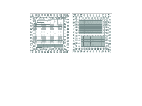
We designed and tested yield vehicles consisting of RQL shift registers with eight Josephson junctions powered by a four-phase AC clock that are triggered sequentially by RQL-encoded data to produce one clock cycle of delay. An exponential progression started with small circuits of just a few stages and moved up to long serpentines that filled the chip (Fig. 1). Such a simple design does not allow faults to be isolated within the circuit, but is adequate for measuring the characteristic maximum size of functional circuits. The chips were designed with density approaching 100,000 devices on a mm die for the SFQ3ee and SFQ4ee integrated circuit processes at the MIT Lincoln laboratory, which represent state-of-the-art superconducting fabrication Tolpygo et al. (2015). However, these processes are only the initial steps on a road-map to much higher densities at more advanced lithography nodes Tolpygo et al. (2014).


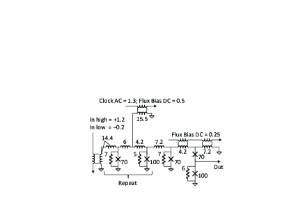
The circuit schematic (Fig. 2) is similar to that reported in Herr et al. (2011). Most of the circuits use junctions with critical currents of 70-100 A, which is half of that previously reported. Only the SFQ3ee four-metal-layer design used the original junction critical currents of 140-200 A. The output circuit is conceptually similar to the SFQ-to-DC converter Likharev and Semenov (1991) but is compatible with RQL data encoding. The output has only three Josephson junctions and produces 0.5 mV, which is adequate for the intended sampling measurement.
Three physical layout styles were developed for two different versions of the fabrication process, SFQ3ee and SFQ4ee, at the MIT Lincoln Laboratory Tolpygo et al. (2015). The two processes have similar feature size but a different number of metal layers. The SFQ4ee process has eight metal layers, M0-M7, while the SFQ3ee process has only four metal layers, M4-M7, corresponding to the topmost layers in the SFQ4ee stack-up. Our various layout styles differ primarily in the choice of ground plane layers in the physical layout.
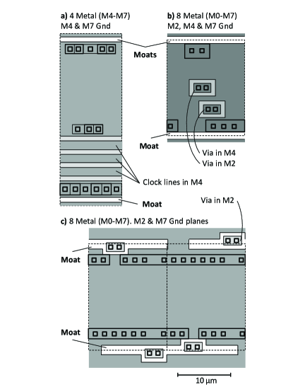
The first layout style uses the SFQ3ee process and is similar to that reported in Herr et al. (2011), but with feature size scaled down to sub-micron design rules. The AC clock lines and bias transformers were laid out beside the Josephson junctions and the interconnect inductors. The active region used two ground planes, M4 and M7, which are the top and bottom metal layers in the stack-up. However, a single ground plane on M7 was used over the clock lines, which were patterned in M4. As this layout style has a mix of single and double ground planes, we will refer to it as having one-and-a-half ground planes. Where two ground planes are present, coincident moats were patterned in both layers. Ground metal for this style is shown (Fig. 3a).

The second layout style, using the SFQ4ee process, had three global ground planes with coincident moats laid out in M2, M4, and M7 (Fig. 3b). More metal layers allowed increased vertical integration. The AC clock lines and bias transformers were laid out in the M0 and M1 metal layers, under the Josephson junctions and the interconnect inductors that used M3, M5, and M6. Additional features were patterned in the M2 and M4 ground planes to accommodate thru-vias, which were intentionally staggered.
The third layout style (Fig. 3c) also used the SFQ4ee process but had only two ground planes, M2 and M7. Thru-vias were placed in the moats. To get above the M2 ground plane, a wire in M1 extended to the via in the moat and a wire in M3 followed the same path back over the ground plane. Coupling from a flux trapped in the moat into the M1/M3 loop would be small as the loop is orthogonal to the moat. Extensive via walls around the moat shield the current associated with trapped flux from the active circuit. Another significant change from the previous layout style is that the moats in this design are only 26 m long and are separated by a 3.6 m gap, instead of being continuous structures with a length scale similar to the dimensions of the circuit, about 3 mm. The shorter moats with gaps are more amenable to the X-Y interconnect needed for more complex logic circuits.
III Test
Chips were mounted in a pressure-contact probe with three concentric mu-metal shields to attenuate ambient field below 1 T, which is an order of magnitude less than the critical field for complete vortex expulsion, T for our typical moat separation, m. The probe was lowered into an LHe transport dewar to achieve the 4.2 K operating temperature. All chips were tested using a manual measurement in which the cooling rate through the transition temperature was neither observable nor well-controlled, but is estimated to have been 0.1-10 K/s. Circuits were tested using a simple repetitive bit sequence from a pattern generator connected to chip input, and output was observed on a sampling oscilloscope after passing through a low-noise amplifier. For convenience, the tests were conducted at a 2 GHz rate, which is much lower than the intrinsic maximum speed of the shift registers. Operating margins on clock power where measured for functional circuits by visually matching the output to the expected bit sequence. The point of circuit failure was somewhat subjective, but is estimated to be accurate to 0.2 dB as the onset of errors is quite rapid.
The largest circuits were retested using an automated measurement with improved test procedures: 1) The analog waveforms from the sampling oscilloscope were downloaded to a PC and digitized using a simple threshold algorithm. Operating margins on clock power where measured using an automated binary search that both compared the digitized output to the expected pattern, and set the clock power produced by the sine-wave generator. 2) The cool-down rate through the transition temperature was controlled using a thermometer and a heater to be about 3 mK/s. This proved to be very important.

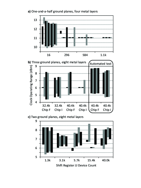
For the one-and-a-half-ground-plane layout style, representative results from one chip are shown in Fig. 4a. On subsequent cooldowns, the 16-junction circuit worked with margins of 2-3 dB with 90% probability, which is sufficient to validate the circuit schematic, fabrication process, and test fixture. However, the probability of a working circuit fell off rapidly with increasing circuit size. The 296-junction circuit showed similar margins with only 20% probability, the 584 junction circuit worked only 10% of the time, with reduced margins, and the 1,136-junction circuit was found to be nonfunctional in six cool-down attempts. This result indicates high flux-trapping incidence compared to a previously-reported circuit of similar junction count and similar layout style, but fabricated with 2 m minimum feature size. Without more data this result would indicate that flux-trapping incidence increases as feature size decreases to sub-micron.
For the three-ground-plane layout style, multiple chips from two wafers were tested. In stark contrast to the previous result, shift registers of all sizes were found to be functional. Test effort was directed to the chips containing the two largest circuits, with 32,400 and 40,400 Josephson junctions, which together filled the 3 mm3 mm active area of the chip. Fig. 4b shows results for two chips, labeled F and I, that are representative of the most favorable and least favorable data collected. For the manual test, operating margins are not reproducible from one cool-down to the next, but only a few attempts are needed in order to establish wide margins. The widest margins are only weakly correlated to circuit size. Taken together, the two circuits on Chip F represent a 72,800 Josephson junction chip with operating margins of 3 dB. This is the largest digital superconducting chip ever reported.
Re-test of the larger circuits using the automated setup is also shown in Fig. 4b. For Chip I, the circuit was found to be functional on all four cool-downs with relatively reproducible margins ranging from 3-3.7 dB. For Chip F the circuit was functional on all five cool-downs with margins that were reproducible to within 0.06 dB, the resolution of the automated binary search. This corresponds to reproducibility of clock amplitude of about 1%. As other factors such as system noise or variable contact resistance in the pressure contact probe could account for this level of variability between cool-downs, the result produced no evidence of flux trapping.
Finally, for the two-ground-plane layout style, data for a single chip collected using manual test are shown in Fig. 4c. The largest circuit, comparable in size to the largest three-ground-plane circuits, was functional on five-of-five cool-downs but with varying operating margins. Overall the data indicate that this layout style had roughly similar effectiveness at sequestering trapped flux in the moats as the three-ground-plane style.
IV Discussion
Our main result is an existence proof of large RQL circuits of up to 72,800 Josephson junctions per die fabricated in an eight-metal-layer sub-micron process operating with large operating margins and showing near-immunity to flux trapping. A circuit with 40,400 Josephson junctions was characterized across five thermal cycles with no evidence of flux trapping, using only the rudimentary precautions of passive mu-metal magnetic shielding and a controlled cool-down rate of 3 mK/s in the test fixture. The relevant metric for flux-trapping statistics in integrated circuits is not junction count per se but active area. We report immunity to flux trapping for circuits with an active area of up to 3 mm square. We expect this result to hold for future circuits with higher density and higher junction count occupying a similar physical area.
We also report very poor performance of circuits fabricated in the four-metal-layer version of the process using one-and-a-half ground planes, which we attribute to flux trapping. Only circuits of less than 600 junctions were found to be functional. By comparison, we previously reported operation of a 1,200-junction circuit with a similar layout style fabricated in a non-planarized, 2 m process Herr et al. (2011). We developed a simple narrative to account for these poor initial results, under the assumptions that the ground planes may have slightly different transition temperatures, and that the ground planes are effectively superconducting before finer features such as vias and wires. If the M7 global ground plane goes superconducting first and sequesters a trapped flux in the moat, it is plausible that the trapped flux will also find the corresponding moat in the M4 half-ground-plane. However, if the M4 half-ground-plane goes superconducting first, the trapped flux may instead be expelled to the slits that are used to define the clock lines. Subsequent trapping in the moat in M7 will cause magnetic field to thread through the active region on the circuit. In this scenario, the moats concentrate field exactly where it is not wanted, and may be worse than no moats at all.
The technological solutions that produced flux-trapping immunity in the largest circuits fall into three general categorizes: 1) the eight-metal-layer, planarized, sub-micron fabrication process, 2) the moat geometry in physical layout, and 3) the slow, controlled cool-down in circuit test. These solutions are expected to be general to all superconductor integrated circuits and do not depend on the particulars of the RQL circuits reported here. The eight-metal-layer process affords vertical integration that eliminates the compromises in layout style that were present in the four-metal-layer design. Planarization avoids film topology that could produce undesirable pinning centers for vortices in the ground plane. Physical layout was centered around moat design done in accordance with the analysis presented in Section I. Long moats with spacing not greater than 15 m were designed to produce complete vortex expulsion from the patterned ground plane. Continuous moats in the three-ground-plane design and perforated moats with 3.6 m spacing in the two-ground-plane design performed equally well. Small de facto moats around the thru-vias in the three-ground-plane design, with maximum dimension of 5 m, did not trap flux with long moats nearby. Even with the best moat design the circuits required a slow cool-down rate. Rapid cool-down reportedly produces thermal gradients leading to EMF currents and magnetic fields in the package Bermon and Gheewala (1983). Since the vortices that form in the ground plane are only large and mobile in a narrow window above the freezing temperature mK, the required cool-down rate may also indicate the time scale for the last vortex to move into the moat.
In conclusion, superconducting digital logic is scalable to increased levels of integration with the development of Reciprocal Quantum Logic and improved fabrication capabilities at sub-micron representing an advance of five process nodes over previously established technology. We report that flux trapping does not appear to be an insurmountable limitation for large-scale superconductor integrated circuits at advanced process nodes. Based on this success, we conclude that further efforts are warranted to scale the technology yet further.
Acknowledgements.
The authors acknowledge communication with Paul Bunyk, Vasili Semenov, and Sergey Tolpygo regarding effective moat geometry, Yuri Polyakov regarding the test fixture, and Mark Gouker regarding the strategy for circuit test.References
- Abelson and Kerber (2004) L. A. Abelson and G. L. Kerber, Proceedings of the IEEE 92, 1517 (2004).
- Herr et al. (2011) Q. P. Herr, A. Y. Herr, O. T. Oberg, and A. G. Ioannidis, Journal of Applied Physics 109, 103903 (2011).
- Herr et al. (2013) A. Y. Herr, Q. P. Herr, O. T. Oberg, O. Naaman, J. X. Przybysz, P. Borodulin, and S. B. Shauck, Journal of Applied Physics 113, 033911 (2013).
- Johnson et al. (2010) M. Johnson, P. Bunyk, F. Maibaum, E. Tolkacheva, A. Berkley, E. Chapple, R. Harris, J. Johansson, T. Lanting, and I. Perminov, Superconductor Science and Technology 23, 065004 (2010).
- Tolpygo et al. (2015) S. K. Tolpygo, V. Bolkhovsky, T. J. Weir, L. M. Johnson, M. A. Gouker, and W. D. Oliver, Applied Superconductivity, IEEE Transactions on 25, 1101312 (2015).
- Bermon and Gheewala (1983) S. Bermon and T. Gheewala, Magnetics, IEEE Transactions on 19, 1160 (1983).
- Nagasawa et al. (1995) S. Nagasawa, H. Numata, C. Kato, and S. Tahara, Extended Abstracts of 5th International Superconductive Electronics Conference 5, 192 (1995).
- Fujiwara et al. (2009) K. Fujiwara, S. Nagasawa, Y. Hashimoto, M. Hidaka, N. Yoshikawa, M. Tanaka, H. Akaike, A. Fujimaki, K. Takagi, and N. Takagi, Applied Superconductivity, IEEE Transactions on 19, 603 (2009).
- Jeffery et al. (1995) M. Jeffery, T. Van Duzer, J. Kirtley, and M. Ketchen, Applied Physics Letters 67, 1769 (1995).
- Robertazzi et al. (1997) R. Robertazzi, I. Siddiqi, and O. Mukhanov, Applied Superconductivity, IEEE Transactions on 7, 3164 (1997).
- Polyakov et al. (2011) Y. A. Polyakov, V. K. Semenov, and S. K. Tolpygo, Applied Superconductivity, IEEE Transactions on 21, 724 (2011).
- Terai et al. (2007) H. Terai, M. Tanaka, Y. Yamanashi, Y. Hashimoto, A. Fujimaki, N. Yoshikawa, and Z. Wang, Applied Superconductivity, IEEE Transactions on 17, 422 (2007).
- Semenov et al. (1999) V. Semenov, Y. A. Polyakov, and W. Chao, Applied Superconductivity, IEEE Transactions on 9, 4030 (1999).
- Polyakov et al. (2007) Y. Polyakov, S. Narayana, and V. K. Semenov, Applied Superconductivity, IEEE Transactions on 17, 520 (2007).
- Narayana et al. (2009) S. Narayana, Y. Polyakov, and V. K. Semenov, Applied Superconductivity, IEEE Transactions on 19, 640 (2009).
- Semenov et al. (2015) V. K. Semenov, Y. Polyakov, and S. K. Tolpygo, Applied Superconductivity, IEEE Transactions on 25, 1301507 (2015).
- Stan et al. (2004) G. Stan, S. B. Field, and J. M. Martinis, Physical Review Letters 92, 097003 (2004).
- Kuit et al. (2008) K. Kuit, J. Kirtley, W. Van Der Veur, C. Molenaar, F. Roesthuis, A. Troeman, J. Clem, H. Hilgenkamp, H. Rogalla, and J. Flokstra, Physical Review B 77, 134504 (2008).
- Pearl (1964) J. Pearl, Applied Physics Letters 5, 65 (1964).
- Clem (1998) J. R. Clem, APS March Meeting Abstracts 1, 3606 (1998).
- Likharev (1972) K. Likharev, Sov. Radiophys 14, 722 (1972).
- Maksimova (1998) G. Maksimova, Physics of the Solid State 40, 1607 (1998).
- Tolpygo et al. (2014) S. K. Tolpygo, V. Bolkhovsky, L. M. Johnson, W. D. Oliver, and M. A. Gouker, Superconductivity News Forum Global Edition 30, STP402 (2014).
- Likharev and Semenov (1991) K. K. Likharev and V. K. Semenov, Applied Superconductivity, IEEE Transactions on 1, 3 (1991).