Transient phases during fast crystallization of organic thin films from solution
Abstract
We report an in-situ microbeam grazing incidence X-ray scattering study of 2,7-dioctyl[1]benzothieno[3,2-b][1]benzothiophene (C8-BTBT) organic semiconductor thin film deposition by hollow pen writing. Multiple transient phases are observed during the crystallization for substrate temperatures up to 93∘C. The layered smectic liquid-crystalline phase of C8-BTBT initially forms and preceedes inter-layer ordering, followed by a transient crystalline phase for temperature 60∘C, and ultimately the stable phase. Based on these results, we demonstrate a method to produce extremely large grain size and high carrier mobility during high-speed processing. For high writing speed (25 mm/s) mobility up to 3.0 cm2/V-s has been observed.
I Introduction
Solution-processed organic semiconductor thin films have attracted great interest due to their potential applications in low-cost and flexible organic electronic devicesSirringhaus (2005). An important challenge lies in the manipulation of morphology and crystalline ordering of molecules, which critically influences the electronic properties of thin films.Lim et al. (2009); Kumar et al. (2014) However, due to the weak Van Der Waals forces between organic semi-conducting molecules, the molecular packing depends sensitively on the processing methods and conditions.Diao et al. (2014) Therefore, understanding the crystallization mechanisms, which turn out to be both subtle and varied, is important to give insight into controlling the deposition processes.
We address the question of whether high-speed pen writing can be optimally used for the fabrication of electronic devices such as organic field effect transistors (OFETs). At high enough speeds, films are deposited in a liquid state that subsequently transforms to a solid due to evaporation of the solvent; this is known as the Landau-Levich-Derjaguin (LLD) regime.Landau and Levich (1942); Derjaguin (1943) Although LLD extends to practically unlimited writing speeds, LLD normally leads to a high nucleation density resulting in an isotropic small-grain structure.Wo, Headrick, and Anthony (2012) This results in grain boundaries and other defects, which introduce trap states that compromise charge carrier mobility. Hence, oriented single-crystalline films are desirable for achieving low defect density, but this normally requires slow writing in the “convective” deposition regime.Headrick et al. (2008); Cour et al. (2013) Thus, there is seemingly no optimal strategy for high-speed processing. Here, we report the discovery of mechanisms that lead to large grain size in the LLD regime, effectively solving this long-standing problem.

II Experiment
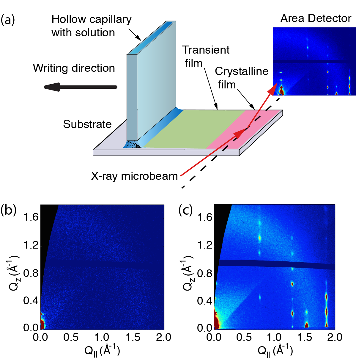
C8-BTBT was synthesized from commercially available 2-chlorobenzaldehyde via the methodology described by Takimiya et al.Ebata et al. (2007); Saito et al. (2011) Heavily doped n-type (100) silicon wafers with a 300 nm thermally grown silicon oxide layer were used as substrates for fabrication of bottom-gate, top-contact OFETs and for the X-ray measurements. We utilize the hollow capillary pen writing method with substrate heating to deposit thin films with controllable thickness and grain morphology.Headrick et al. (2008) Real-time polarized optical microscopy (POM) was utilized to study the sequence of phases formed and the evolution of the grain morphology. In-situ microbeam grazing incidence wide-angle X-ray scattering (GIWAXS) was carried out for the same process at the Cornell High Energy Synchrotron Source (CHESS) at beamline D1. The X-ray wavelength was = 1.155 Å. A schematic of the layout is shown in Fig. 1.Smilgies et al. (2013) The X-ray intensities are plotted in Fig. 1(b, c) as a function of the in-plane component of the wavevector transfer and the component perpendicular to the substrate surface . Further details of the device fabrication and X-ray setup are given in the Supplementary Information file.Sup
III Results and Discussion
We have obtained a room temperature average OFET mobility of 4.0 cm2/V-s for aligned C8-BTBT thin films deposited in the convective regime at 0.5 mm/s (Supplementary Fig. S1).Sup This result is in good agreement with a previous report of 3.5 - 5 cm2/V-s by Uemura et al. for oriented films prepared by directed solution deposition on SiO2/doped Si substrates.Uemura et al. (2009) Remarkably, we find that nearly comparable results – 2.7 cm2/V-s average and 3.0 cm2/V-s peak – can be obtained in the LLD regime at 25 mm/s if the substrate is held at 60∘C. As we discuss below, real-time POM and GIWAXS show that a series of transformations takes place that is consistent with Ostwald’s rule of stages.Ostwald (1897) A key finding is that the grain size is controlled by the nucleation rate during the transformation from a transient liquid crystalline (LC) state to the crystalline form, and that the nucleation rate conforms to predictions of classical nucleation theory.Porter, Easterling, and Sherif (2009) For deposition temperatures up to 60∘C, LC transforms directly to the stable crystalline form Cr2 (see Supplementary Fig. S2).Sup However, above 60∘C, a new intermediate crystalline state (Cr1) briefly forms, which leads to cracking of the films due to tensile strain as the final stable phase (Cr2) forms.
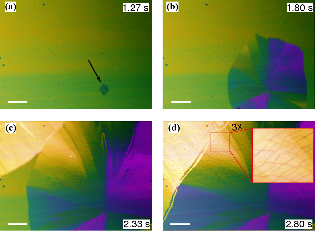
In Fig. 2, four frames from a polarized microscope movie for deposition at 90∘C substrate temperature are presented. Note that the substrate moves instead of the pen for these observations (while it is the pen that moves for the X-ray results). However, it has already completed its motion by the time of Fig. 2(a) at = 1.27 s relative to the time the area in view was written. Fig. 2(a) shows that a crystalline nucleus suddenly appears in the field of view. The drying of the film (not shown) occurs very fast, so the main part of the film visible in Fig. 2(a), is interpreted as the LC phase. The LC phase is only stable above 95∘C, so in this sequence it effectively exists in a supercooled state. A crystalline phase subsequently nucleates after a temperature-dependent incubation time. In Fig. 2(b) and (c) the crystalline grain expands in all directions. Cracks are observed to progressively form in Fig. 2(c) and (d). In Supplementary Movie 1,Sup the cracks are observed to sweep radially outward from the original nucleation center, which we interpret as the transition from Cr1 to Cr2. As we discuss below, cracks degrade the performance of OFET devices even though the film has millimeter-scale grains.
Fig. 3 shows the results of an in-situ crystallization study. The integrated intensities of the major Bragg peaks as a function of time during the deposition is shown in Fig. 3(a) and (e) for films written at 25 mm/s at 85∘C and 90∘C respectively. The rapid growth of the (001) reflection (blue data points and line in each case) starts almost right after the first dashed vertical line, which indicates = 0 when the X-ray beam starts to hit the film after the pen passes by it. Subsequently, the (001) reflection exists alone for quite some time. During this time interval, the diffraction pattern is consistent with a smectic liquid crystal state, with layered structure perpendicular to the plane of the surface, but lacking any in-plane long-range order.Gbabode et al. (2014) Moreover, we clearly observe that at 90∘C, the time interval of the LC state is longer than at 85∘C. The crystalline phases start to appear after the second vertical dashed line in Fig. 3(a) and (e). Note that an intermediate crystalline phase Cr1 is briefly observed, but it transforms to Cr2 in less than one second. Fig. 3(c, d, g) shows that Cr2 forms with the (11L) peaks shifted in both and relative to Cr1. It is significant that Cr2 is at higher , which corresponds to a closer crystalline packing in the plane of the film. This transition between solid phases evidently introduces a high () strain in the plane of the film that leads to mechanical failure and cracking of the films, as we have observed by POM in Fig. 2(d). The shift in is interpreted as a shift in the stacking angle, coresponding to the angle of the unit cell. After the film was cooled down to room temperature the positions of X-ray reflections were shifted due to thermal expansion (see Supplementary Fig. S3).Sup The final positions are close to the bulk phase (see Supplementary Tables 1 2).Sup
In Fig. 4, we plot the time interval between the formation of the intermediate liquid crystal phase and the first appearance of (11L) in-plane reflections at different substrate heating temperature. The trend is that it stays in the smectic phase longer at higher temperatures. We use a simple nucleation model to fit the data where the nucleation rate has the form , where is the Gibbs free energy nucleation barrier, is Boltzmann’s constant, is the temperature.Porter, Easterling, and Sherif (2009) Here, , where is the undercooling below the equilibrium transition temperature. This expression shows that when becomes small, the nucleation rate drops exponentially, and hence the incubation time increases rapidly. But the crystallization velocity seems to be hardly affected, so that a low nucleation rate generally leads to a very large grain size.
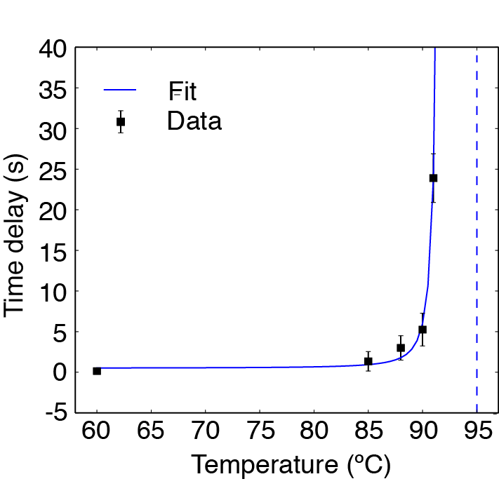
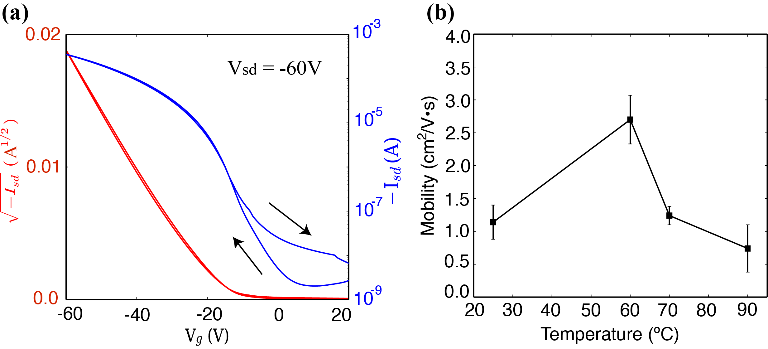
Fig. 5 presents carrier mobility for deposition at 25 mm/s at different substrate temperature and the corresponding film morphology is shown in Supplementary Fig. S5.Sup The grain size increases with temperature, which correlates with the increasing mobility up to 60∘C where, as we have discussed above, no Cr1 phase is observed and thus there is no cracking related to the Cr1Cr2 phase transition. We have also found that no cracking occurs for film thicknesses below 20 nm at 80∘C, which indicates that it is possible to stabilize the Cr1 metastable form (see Supplementary Fig. S6).Sup
The formation of transient phases during crystallization is an example of Ostwald’s rule of stages,Ostwald (1897) which is based on the empirical observation that thermodynamically unstable phases often form before the stable phase during crystallization from solution. For such a sequence to occur, the transient phases must have lower activation barriers for nucleation compared to the stable phase,Chung et al. (2009) where the th nucleation barrier originates from the interface energy at the boundaries between successive phases and . It is attractive to consider this transition in terms of reduced symmetry: for example, the LC phase is structurally similar to the isotropic phase except for the loss of translational symmetry along the layering direction plus a degree of orientational ordering of the molecules. Similarly, the crystalline phase loses translational symmetry in the plane of the layers, and thus becomes even less similar to the original isotropic state. Thus, it is reasonable that the isotropicLC transition has a lower nucleation barrier compared to the direct isotropicCr transition because more similar structures should have comparatively lower interface energies between them. Based on this argument, the configurational entropy of the system is also lowered, so the order of appearance of phases more fundamentally follows a rule of decreasing entropy, where the phase formed at each stage is the one with the smallest entropy change. One prediction of this rule is that any material that has an LC phase should transform to the LC phase before reaching its crystalline form.
IV Conclusions
We have described the formation of transient phases of C8-BTBT thin films during solution processing at high speed. Although striking and somewhat surprising, the results of POM, in-situ GIWAXS, and OFET studies point to a model that is entirely consistent with classical nucleation theory and with Ostwald’s rule. These results lead to a method to produce extremely large grain size films and high carrier mobility in the LLD regime that may prove to be of considerable practical importance. We predict that many additional materials will be found to exhibit high-symmetry transient phases, particularly those that can form an LC phase.
Acknowledgements.
This work was supported by the National Science Foundation, Division of Materials Research, Electronic and Photonic Materials Program through award DMR-1307017. The X-ray scattering research was conducted at the Cornell High Energy Synchrotron Source (CHESS) which is supported by the NSF and the National Institutes of Health/National Institute of General Medical Sciences under NSF award DMR-1332208.References
- Sirringhaus (2005) H. Sirringhaus, “Device physics of solution-processed organic field-effect transistors,” Advanced Materials 17, 2411–2425 (2005).
- Lim et al. (2009) J. A. Lim, H. S. Lee, W. H. Lee, and K. Cho, “Control of the morphology and structural development of solution-processed functionalized acenes for high-performance organic transistors,” Advanced Functional Materials 19, 1515–1525 (2009).
- Kumar et al. (2014) P. Kumar, K. N. Shivananda, W. Zajaczkowski, W. Pisula, Y. Eichen, and N. Tessler, “The relation between molecular packing or morphology and chemical structure or processing conditions: the effect on electronic properties,” Advanced Functional Materials 24, 2530–2536 (2014).
- Diao et al. (2014) Y. Diao, K. M. Lenn, W.-Y. Lee, M. A. Blood-Forsythe, J. Xu, Y. Mao, Y. Kim, J. A. Reinspach, S. Park, A. Aspuru-Guzik, G. Xue, P. Clancy, Z. Bao, and S. C. B. Mannsfeld, “Understanding polymorphism in organic semiconductor thin films through nanoconfinement,” Journal of the American Chemical Society 136, 17046–17057 (2014).
- Landau and Levich (1942) L. Landau and B. Levich, “Dragging of a liquid by moving plate,” Acta Physicochimica URSS 17, 42 (1942).
- Derjaguin (1943) B. Derjaguin, “Thickness of liquid layer adhering to walls of vessels on their emptying and the theory of photo- and motion picture film coating,” C.R. (Dokl.) Acad. Sci. URSS 39, 13–16 (1943).
- Wo, Headrick, and Anthony (2012) S. Wo, R. L. Headrick, and J. E. Anthony, “Fabrication and characterization of controllable grain boundary arrays in solution-processed small molecule organic semiconductor films,” Journal of Applied Physics 111, 073716 (2012).
- Headrick et al. (2008) R. L. Headrick, S. Wo, F. Sansoz, and J. E. Anthony, “Anisotropic mobility in large grain size solution processed organic semiconductor thin films,” Applied Physics Letters 92, 063302 (2008).
- Cour et al. (2013) I. Cour, P. V. Chinta, C. M. Schlepütz, Y. Yang, R. Clarke, R. Pindak, and R. L. Headrick, “Origin of stress and enhanced carrier transport in solution-cast organic semiconductor films,” Journal of Applied Physics 114, 093501 (2013).
- (10) See supplemental material at [URL will be inserted by AIP] for video files, detailed experimental procedures, supplementary figures, and a table of X-ray peak positions.
- Ebata et al. (2007) H. Ebata, T. Izawa, E. Miyazaki, K. Takimiya, M. Ikeda, H. Kuwabara, and T. Yui, “Highly soluble [1]benzothieno[3,2-b]benzothiophene (BTBT) derivatives for high-performance, solution-processed organic field-effect transistors,” Journal of the American Chemical Society 129, 15732–15733 (2007).
- Saito et al. (2011) M. Saito, I. Osaka, E. Miyazaki, K. Takimiya, H. Kuwabara, and M. Ikeda, “One-step synthesis of [1]benzothieno[3,2-b][1]benzothiophene from o-chlorobenzaldehyde,” Tetrahedron Letters 52, 285 – 288 (2011).
- Smilgies et al. (2013) D.-M. Smilgies, R. Li, G. Giri, K. W. Chou, Y. Diao, Z. Bao, and A. Amassian, “Look fast: Crystallization of conjugated molecules during solution shearing probed in-situ and in real time by x-ray scattering,” physica status solidi (RRL) –Rapid Research Letters 7, 177–179 (2013).
- Uemura et al. (2009) T. Uemura, Y. Hirose, M. Uno, K. Takimiya, and J. Takeya, “Very high mobility in solution-processed organic thin-film transistors of highly ordered [1]benzothieno[3,2-b]benzothiophene derivatives,” Applied Physics Express 2, 111501 (2009).
- Ostwald (1897) W. Ostwald, “Studies on formation and transformation of solid materials,” Z. Phys. Chem 22, 289–330 (1897).
- Porter, Easterling, and Sherif (2009) D. A. Porter, K. E. Easterling, and M. Y. Sherif, Phase Transformations in Metals and Alloys, 3rd ed. (CRC Press, 2009).
- Gbabode et al. (2014) G. Gbabode, M. Dohr, C. Niebel, J.-Y. Balandier, C. Ruzié, P. Négrier, D. Mondieig, Y. H. Geerts, R. Resel, and M. Sferrazza, “X-ray structural investigation of nonsymmetrically and symmetrically alkylated [1]benzothieno[3,2-b]benzothiophene derivatives in bulk and thin films,” ACS Applied Materials Interfaces 6, 13413–13421 (2014).
- Chung et al. (2009) S.-Y. Chung, Y.-M. Kim, J.-G. Kim, and Y.-J. Kim, “Multiphase transformation and Ostwald’s rule of stages during crystallization of a metal phosphate,” Nat Phys 5, 68–73 (2009).