From Fowler-Nordheim to Non-Equilibrium Green’s Function Modeling of Tunneling
I Abstract
In this work, an analytic model is proposed which provides in a continuous manner the current-voltage characteristic (I-V) of high performance tunneling field-effect transistors (TFETs) based on direct bandgap semiconductors. The model provides closed-form expressions for I-V based on: 1) a modified version of the well-known Fowler-Nordheim (FN) formula (in the ON-state), and 2) an equation which describes the OFF-state performance while providing continuity at the ON/OFF threshold by means of a term introduced as the ”continuity factor”. It is shown that traditional approaches such as FN are accurate in TFETs only through correct evaluation of the total band bending distance and the ”tunneling effective mass”. General expressions for these two key parameters are provided. Moreover, it is demonstrated that the tunneling effective mass captures both the ellipticity of evanescent states and the dual (electron/hole) behavior of the tunneling carriers, and it is further shown that such a concept is even applicable to semiconductors with nontrivial energy dispersion. Ultimately, it is found that the I-V characteristics obtained by using this model are in close agreement with state-of-the-art quantum transport simulations both in the ON- and OFF-state, thus providing validation of the analytic approach.
II Introduction
Due to the increasing role of band-to-band tunneling (BTBT) and Schottky barrier (SB) tunneling mechanisms in electronic devices, it becomes critical to develop analytic models that allow identifying the key parameters which optimize the tunneling performance. One of the most promising tunneling device concepts is the tunneling field-effect-transistor (TFET) [1, 2, 3] whose performance can be significantly boosted by aggressively scaling down its dimensions (referred to as high performance TFETs) [4, 5]. The importance of tunneling is not limited to the tunneling devices but it also affects the performance of ultra-scaled FETs significantly [6].
Many approaches to TFET modeling are based on the numerical evaluation of the Wentzel-Kramers-Brillouin (WKB) approximation [10, 9, 11, 7, 8]. The WKB method has been found to be an appropriate description for TFETs based on direct bandgap semiconductors with a single dominant tunneling path if the WKB inputs, namely analytic potential profile and complex bandstructure, are close to those obtained from self-consistent atomistic calculations [7, 8]. In other works the WKB approximation has been solved analytically for a triangular potential barrier which leads to the traditional Fowler-Nordheim (FN) tunneling transmission expression [20, 12, 13].
| (1) |
where is the elementary charge, is the reduced Planck constant, is the electric field in the transition region from source to channel, is the bandgap of the semiconductor, is the ”tunneling effective mass”.
It is commonly assumed that =, where is the so called ”reduced effective mass” [18]. This approach has been used in previous TFET modeling efforts [10, 12, 13, 14, 15]. Assuming = implies that the complex bands within the bandgap of the semiconductor are parabolic. In other works, is assumed to be either the conductivity effective mass [11, 16], or is simply treated as a fitting parameter [21, 17]. In this study it is shown that the appropriate definition of allows a more realistic description of 1) the ellipticity of the complex bandstructure inside the bandgap (not parabolic) and, 2) the electron/hole duality of tunneling carriers, which have both shown to be key components in modeling the BTBT process [22].
In addition, the correct evaluation of the ”total band bending distance ()”, another key parameter in the FN formula, is discussed for different types of junctions. The use of and leads to a modified FN formula which improves its accuracy in the calculation of tunneling transmission in the ON-state of TFETs.
A new analytic model is ultimately presented based on 1) a modified version of the well-known Fowler-Nordheim (FN) equation for the on-state, 2) a new OFF-current formula which accounts for the direct tunneling from source to drain, while providing a smooth ON-OFF transition through the introduction of a ”continuity factor”. The combination of these analytic approaches allows describing the current-voltage characteristics (I-V) both in the ON- and OFF-state of the device by use of simple and closed-form expressions. The results provided by the analytic model are in close agreement with state-of-the-art full-band numerical simulations using the Non-Equilibrium Green’s Function (NEGF) formalism.
III Tunneling effective mass
Previously, it has been demonstrated that the complex part of the band-structure is an elliptic curve (not parabolic) which is composed of two parts: one dominated by hole behavior, and another by electron behavior. Such an elliptic curve can be described by an analytic formula within 1.4% error compared to rigorous tight-binding simulations [22]. It can be mathematically proven that by taking into account the ellipticity of the complex bands and by assuming a constant electric field in the tunneling window, the tunneling transmission is given by (see Appendix A for details)
| (2) |
where is the reduced effective mass:
| (3) |
Note that (2) is almost identical to the transmission probability equation derived in the 1D case by Kane except for a prefactor of [18, 19]. Therefore, the Kane’s approach takes into account the elliptic complex band structure precisely even for materials with . Through direct comparison, one can realize that equations (1) and (2) are equivalent expressions if the following condition is satisfied:
| (4) |
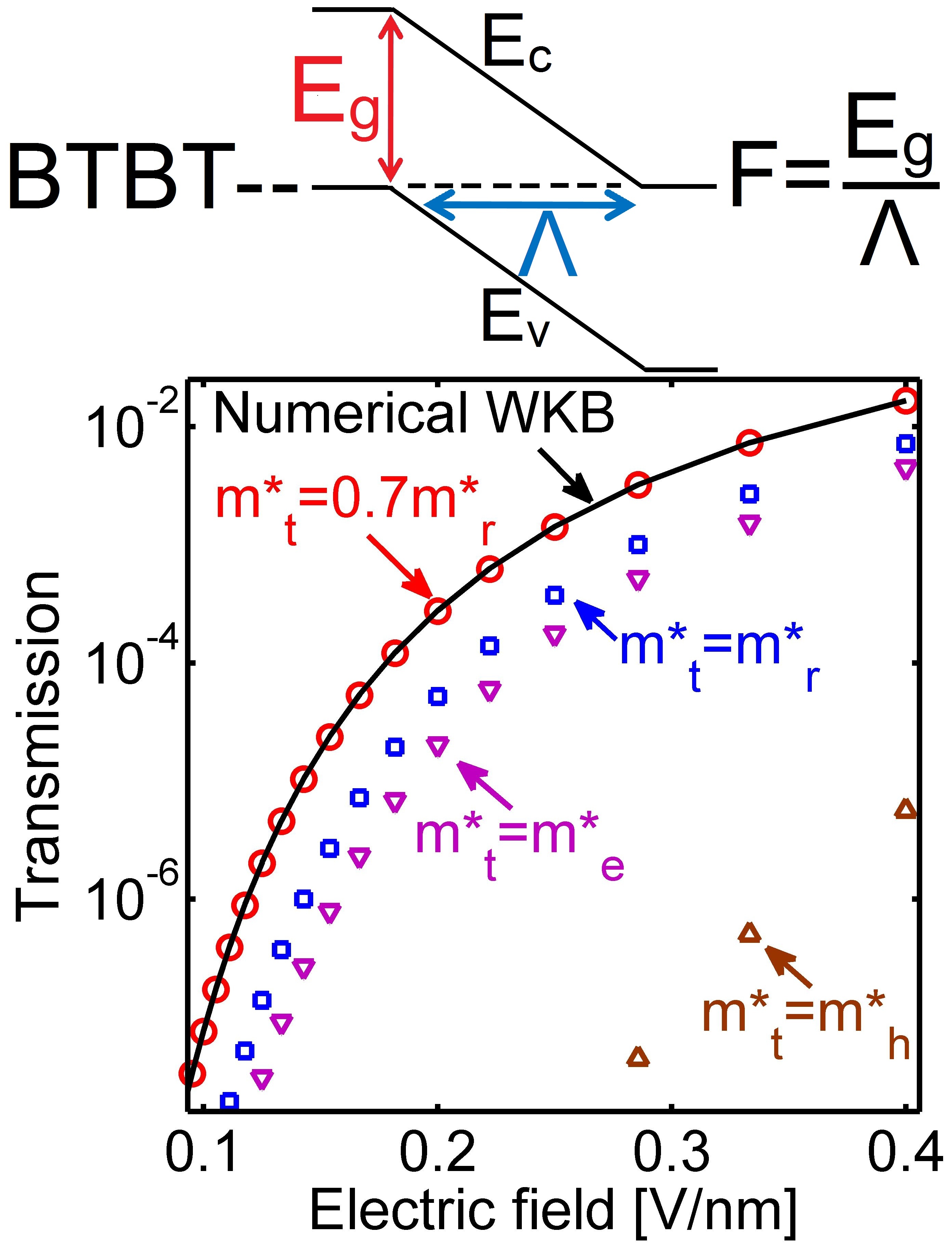
In other words, equation (1) can capture the elliptic nature of the complex bandstructure if indeed from (4) and NOT from (3) is used. This also corrects the notion that the concept of effective mass cannot be applied to BTBT due to the dual electron/hole behavior of carriers as they tunnel through the bandgap [23]. For illustration purposes, Fig. 1a compares the BTBT transmission obtained using different choices of for a material with == and =. The results obtained using = matches well with the numerical WKB calculation, whereas the other conventional choices of (i.e. = or =) lead to a significant error.
To further elucidate the practical advantage and general applicability of the concept of the tunneling effective mass, we consider two examples: 1) graphene nanoribbons (GNRs) with non-trivial energy dispersion and 2) metal-semiconductor Schottky barriers (SBs). It is well established that for GNRs, the band edge effective mass is given by [32], where is the group velocity of carriers within the energy range in which the dispersion is linear. By combining (1), (3) and (4) and using = = due to the symmetry in the energy dispersion, the expression shown in equation (5) is obtained. It is noteworthy that (5) matches exactly the result reported in previous studies but found through more convoluted arguments [23, 24].
| (5) |
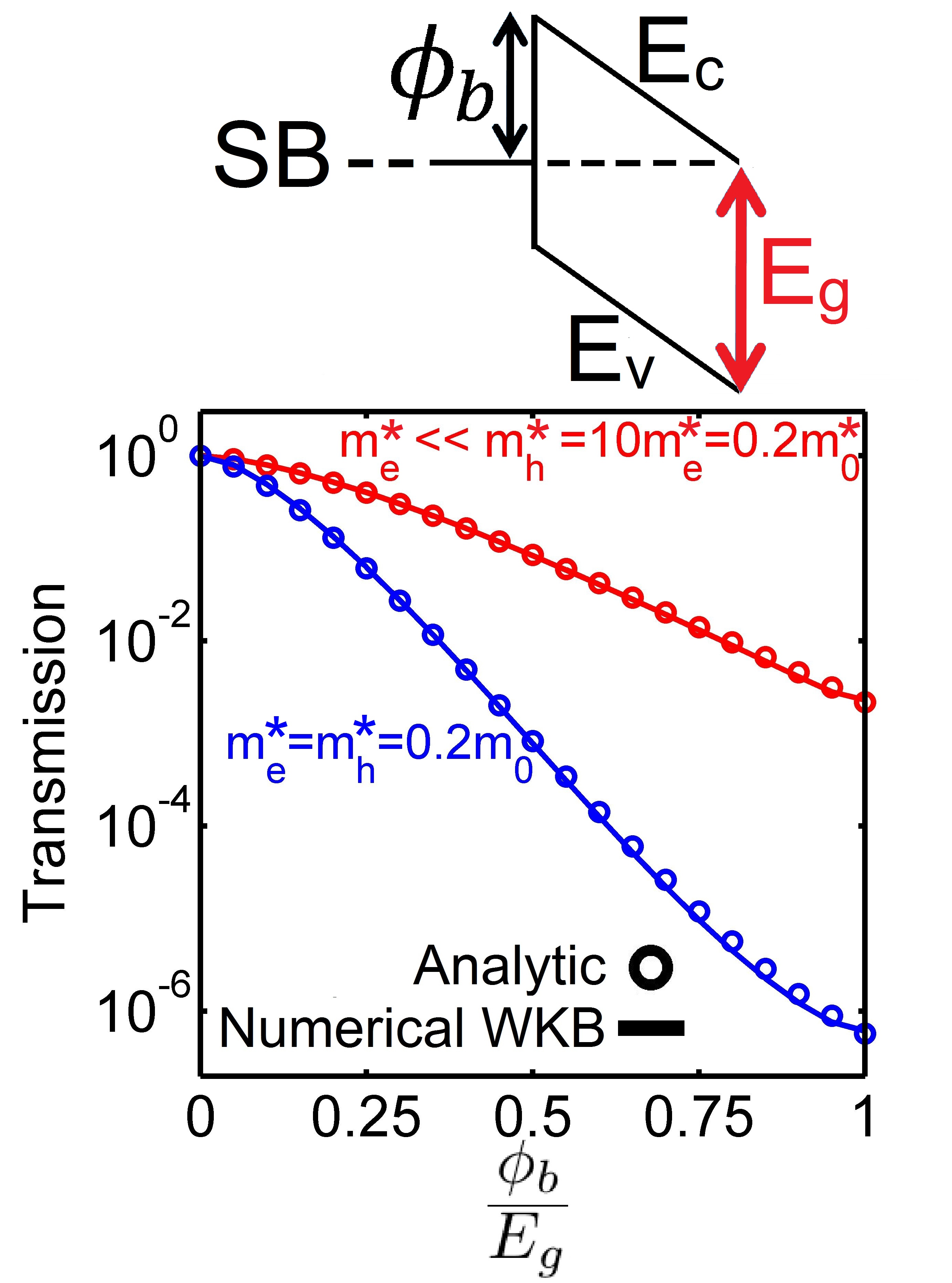
The equation for can also be generalized to metal-semiconductor junctions where the injected carrier tunnels only through a portion of the band gap () as shown in Fig. 1b (see Appendix B for details).
| (6) |
Notice that (6) should be used in the FN equation (1) using instead of . Equation (6) has a simple interpretation; when is small, tunneling occurs in the electron branch of the complex bandstructure, close to the conduction band edge, and hence , whereas for large , reduces to the above reported BTBT result: . The analytic value of the tunneling transmission through a SB using (1) and (6) is found to be in good agreement with the numerical evaluation of the transmission using the WKB approximation as shown in Fig. 1b for both cases of (blue) and (red).
IV Junction electric field
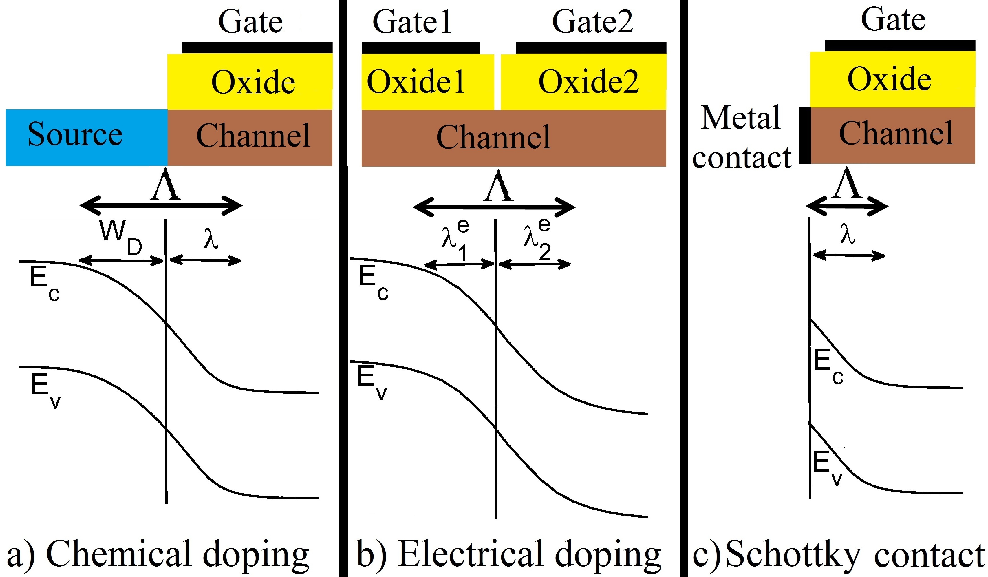
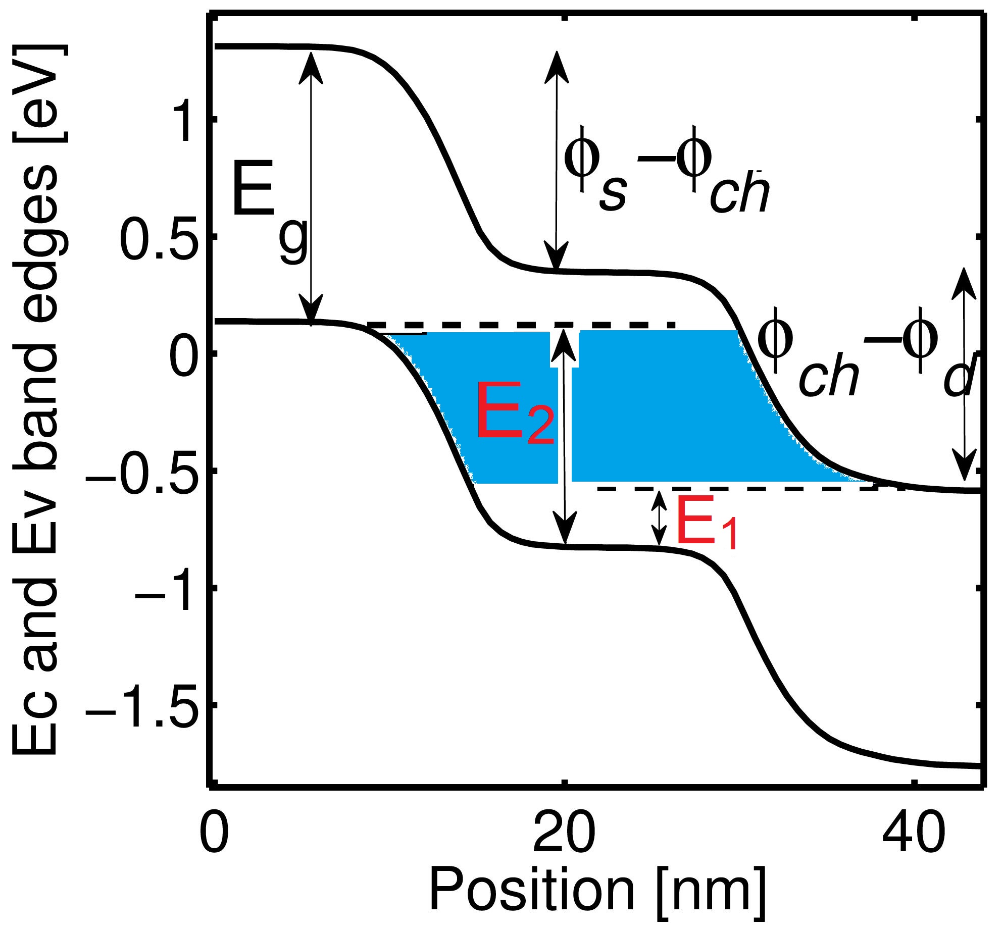
In addition to the tunneling effective mass, the electric field at the tunnel junction plays an important role in the tunneling transmission probability. The electric field magnitude depends on the junction configuration. i.e. the junction can be made in different ways: a gated channel in conjunction with a source/drain contact which is: 1) chemically doped, 2) electrically doped, or 3) a metal. The electric field can be quantified in terms of the source-to-channel band bending distance. Fig. 2 shows the components of bending distance in different junction configurations (i.e. scaling length and depletion width ).
Lee’s scaling length theory [25] can be used to evaluate the bending distance under the gate. According to theory [25, 26, 27, 29] the potential under the gate decays as , where is the ”natural scaling length” and is known for different geometric architectures. For example, in cylindrical nanowire FETs, is given by [27]:
| (7) |
where , and are the dielectric constants of the channel and the oxide respectively, while , and are their thicknesses.
Usually, the bending distance in the source/drain region is ignored. However, it was shown by us that for high performance ultra-scaled TFETs the band bending distance in the source/drain contact is important and in many cases is dominant compared with [8]. The equations for the bending distance in different junction configurations shown in Fig. 2 are:
| (8) |
where is the total band bending distance and is the depletion width of the doped contact [8]. Although different scaling theories are proposed for nanowire TFETs [27, 28], the difference between values is much smaller than even for highly doped TFETs [8] and hence does not vary significantly. Notice that the equation for the scaling length is different in electrically doped devices (distinguished by superscript ) compared to chemically doped devices [29, 30, 31].
| (9) |
where is the total thickness of the device (e.g. in the case of double-gated electrically doped TFETs) and is the spacing between the gates [29].
V Analytic current equation for TFET
In this section, a model which provides the I-V of TFETs through a closed-form equation is presented. In the ON-state, this model uses the modified FN formula. Whereas in the OFF-state, the direct tunneling is combined with a term called the ”continuity factor” which ensures the continuous ON/OFF transition. Finally, the complete I-V model is presented based on the combination of the ON and OFF state analytic expressions.
V-A ON-state
Considering the correct tunneling effective mass and the total bending distance , the equation for current in the ON-state of the device can be written by combining the modified FN formula with the Landauer approach:
| (10) |
where , and are the electrostatic potentials at the source, and channel, respectively. Notice that the difference in source and drain Fermi functions in the Landauer formula is assumed to be 1 (=1) in the tunneling window (i.e. , see Fig. 6). The expression shown in (10) is applicable in the ON-state of the device where . The ON-OFF transition is slightly shifted by (defined in section VI) to have a continuous transition in I-V.
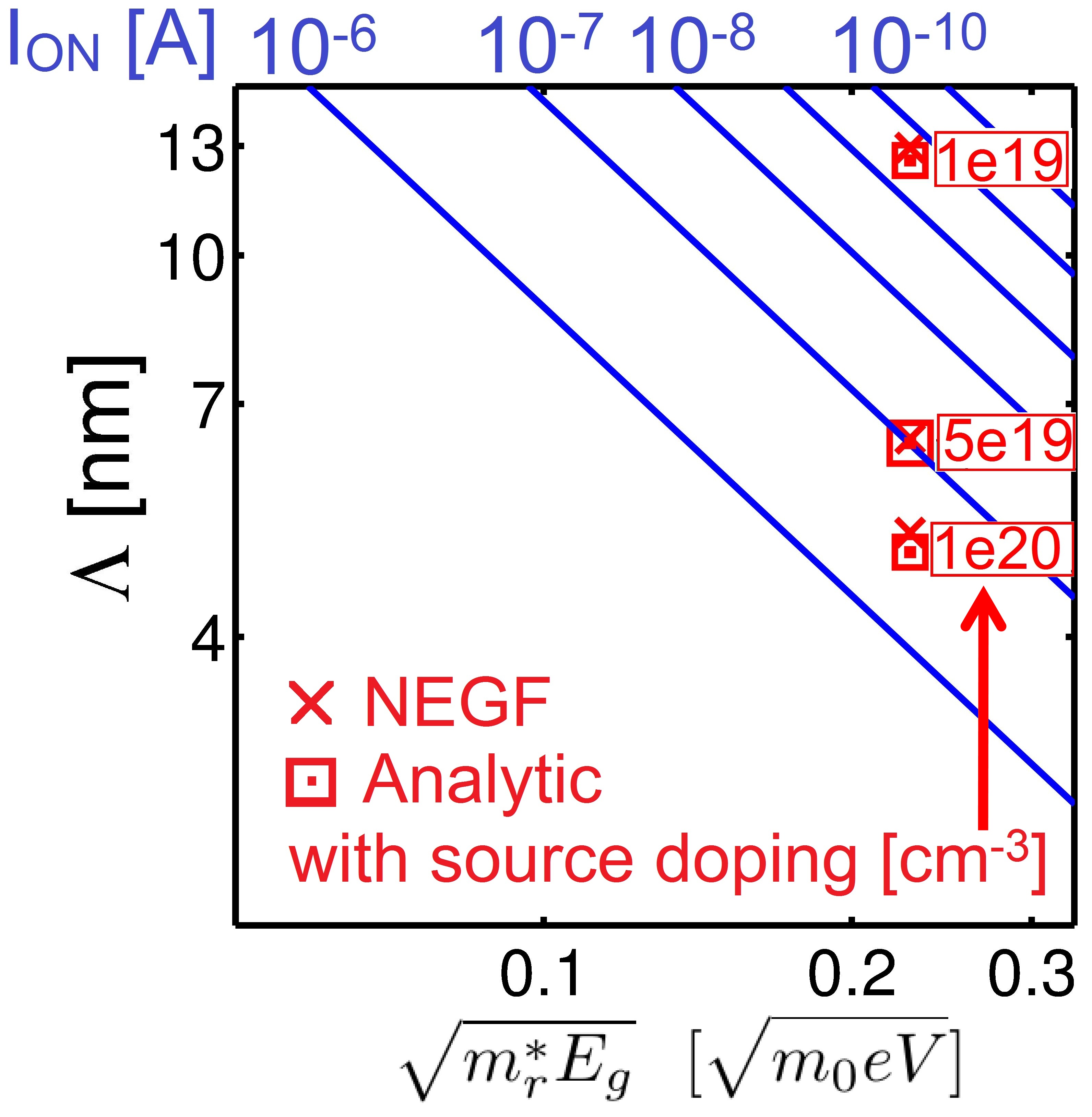
The maximum achievable current () in a TFET can be obtained by combining (4) and (10) and evaluating the result at (i.e. ).
| (11) |
where is the ON-current efficiency factor and is the overdrive ratio defined as
| (12) |
| (13) |
Equation (12) shows how the device design (through ) and the channel material (through and ) can impact the performance of the device. Fig. 3 shows constant current lines (constant ) as a function of and . These constant current curves provide a practical guideline to assess the impact of the channel material and device design on the ON-current in a quantitative manner. In order to illustrate the accuracy and usefulness of this approach, the ON-currents of InAs nanowire TFETs with three different source doping levels are plotted in Fig. 3. Notice that for the same bias conditions () and the same type of device (InAs nanowire TFET) a change in source doping and accordingly in leads to several orders of magnitude of change in ON-current, which is found to be in good agreement with the NEGF simulations [29].
V-B OFF-state
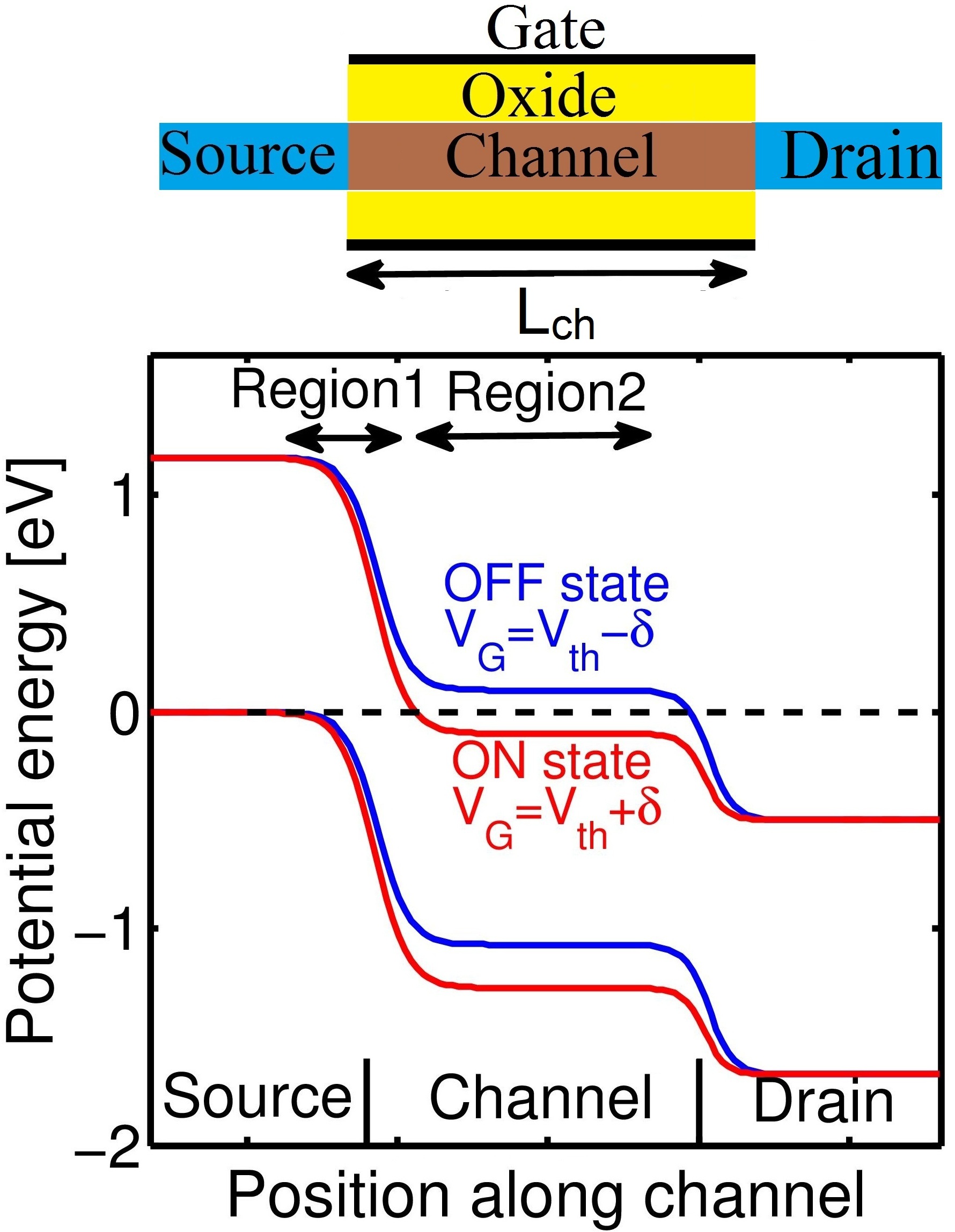
The tunneling current in the OFF-state of the device () between source and drain in its general form is given by (see Fig. 6 in Appendix C)
| (14) |
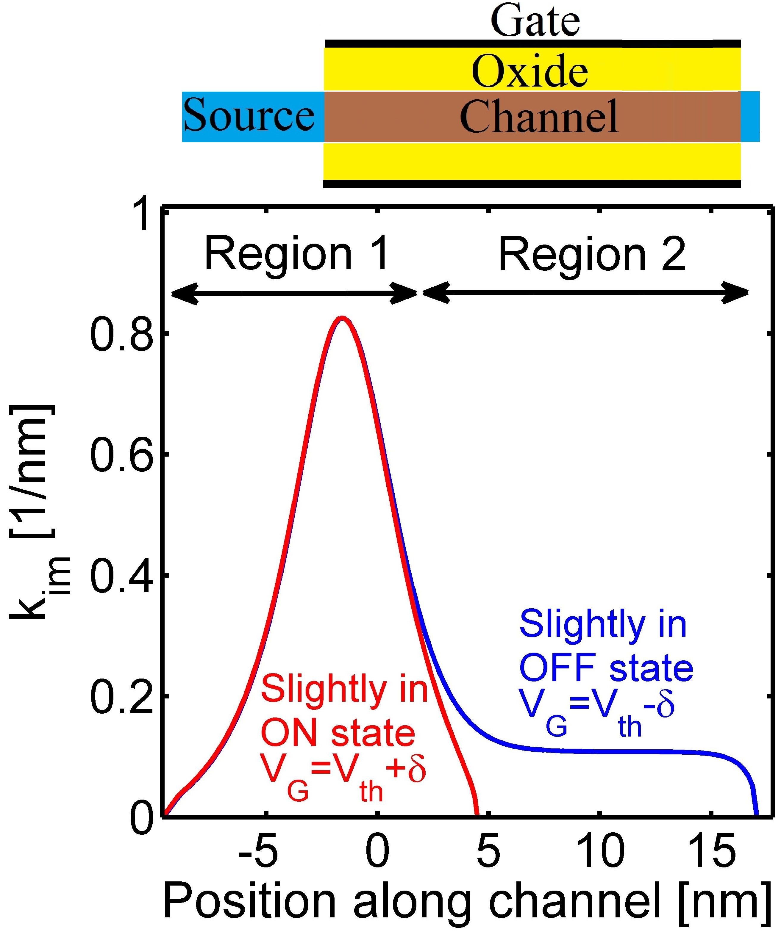
The tunneling in the OFF-state occurs within 2 different regions: 1) a nearly triangular barrier at the source-channel interface and 2) a constant barrier with an approximate length equal to the channel length, as shown in Fig. 4a.
| (15) |
where is the effective channel length (i.e. [8]). Often, the first term (which is related to the crest shown in Fig. 4b) is ignored in the OFF-current calculations because in the case of long devices or bias conditions deep into the OFF-state, is much smaller than and determines the OFF-current. However, for aggressively scaled devices and for bias conditions close to threshold this term is quite important. This term also ensures current continuity at the ON/OFF threshold and thus is called the continuity factor . The value of can be found as follows: close to threshold the term because (see Fig. 4a and 4b). In addition, using (2) close to threshold where leads to . Deep into the OFF-state the term approaches because is spatially constant throughout the channel. Therefore, the general form of the tunneling transmission in the OFF-state reads as:
| (16) |
Evaluating the integral over energy as in (14), leads to (see Appendix C for details)
|
|
(17) |
where is the electrostatic potential at the drain and the function is defined in Appendix C.
VI Results and Comparisons
In order to validate the model, the results of the analytic approach are compared against the full-band quantum transport simulations of an ultra-scaled InAs nanowire TFET with a diameter of 3.4nm, a channel length of 15nm, and an oxide thickness of 1nm. The InAs nanowire is described by a tight-binding model. The numerical simulations are based on a self-consistent solution of the Poisson-NEGF equations using the nanodevice modeling tool NEMO5 [39, 40, 41]. Figure 5 shows the comparison of BTBT I-V (transfer) characteristic at of 0.5V for three different source/drain doping values. The results have been obtained by NEGF (lines) and the analytic model (circle symbols) which is presented in equation (18) given by the combination of (10) and (17) (ON- and OFF-state respectively):
|
|
(18) |
where and are defined in Appendix C and equals (the other parameters have been previously introduced).
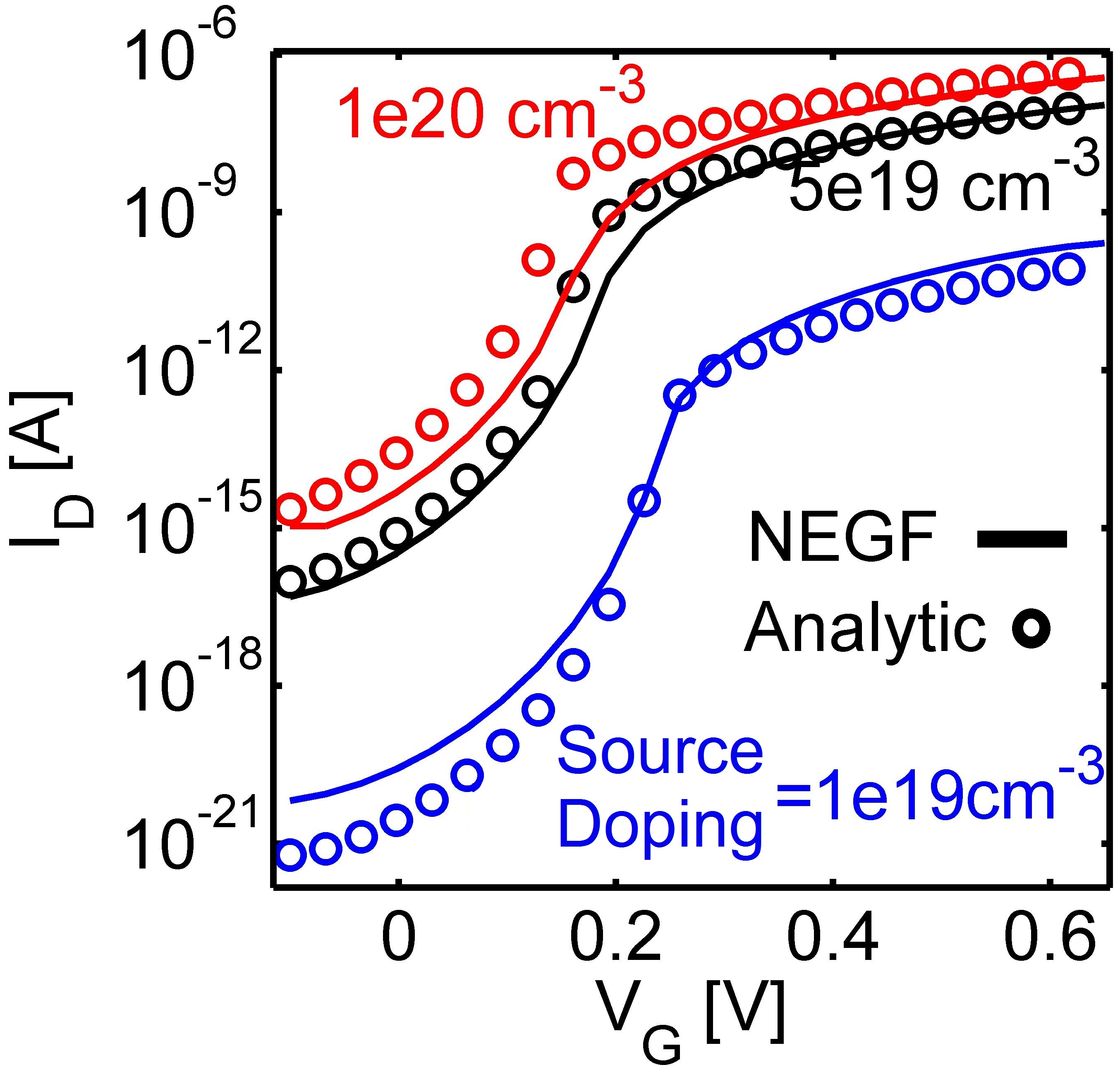
It is clear that the compact model given by (18) reproduces with good accuracy and in a continuous fashion the results obtained through NEGF both in the ON- and OFF-state of the device. The input parameters of the analytic approach are: , , , , and . The three former are material dependent quantities while the latter two are determined by the device design. Notice that due to the low density-of-sates (DOS) of the channel material (InAs), the relation between channel-potential and gate-voltage is close to one-to-one. If a channel material with a high DOS is chosen, the model still provides the current vs. channel-potential characteristic but a capacitor network (series of oxide [33], quantum [5, 12, 34, 35], and offset [36] capacitances) is needed to translate the channel-potential into a gate-voltage.
Therefore, the proposed analytic model enables the quantitative prediction and analysis of material and geometry dependence of the full I-V characteristics of high performance TFETs in direct bandgap semiconductors. Notice that this analytic approach captures most of the relevant tunneling phenomena in TFETs without relying on arbitrary fitting parameters. Thus the model provides a simple and useful alternative to exact numerical methods such as NEGF which have high computational burden.
VII Conclusion
In this work, new expressions have been introduced to describe two key parameters of the tunneling transmission in tunneling devices: the tunneling effective mass and the total band bending distance . The equations for and have been provided in metal-semiconductor (SB tunneling) and p-n junctions (BTBT). It has been proven that the concept of tunneling effective mass not only captures both the ellipticity of the complex bands and the electron/hole dual behavior, but it can also be applied to unconventional semiconductors such as GNRs. The combination of and leads to a modified FN formula which is more accurate for the calculation of BTBT currents in the ON-state of TFETs. Moreover, a new equation has been provided to describe the OFF-state performance of TFETs while providing a continuous transition at the ON-OFF threshold using the continuity factor. Ultimately, the results of the new analytical model are shown to be in good agreement with full band quantum transport simulations both in the ON- and OFF-state of the TFET. The analytic equations reveal that both ON- and OFF-currents decay exponentially with . Accordingly, the channel material of TFETs needs to have an optimum to satisfy the required and .
Appendix A BTBT effective mass
An accurate calculation of band-to-band tunneling transmission requires considering the elliptic nature of the complex band structure (decaying states). Notice that the total transmission depends exponentially on , . The complex wave-vector has electron and hole like regions with transition energy of .
| (19) |
Using the analytic equations for an elliptic complex band structure [22], one can derive:
| (20) |
Evaluation of the integral leads to:
| (21) |
| (22) |
Appendix B Effective mass for Schottky barriers
In this section is derived for a SB with a barrier height of for electrons. The elliptic complex band in the electron branch is described by [22]:
| (23) |
A parabolic approximation to (23) is given by
| (24) |
where and is a constant (in units of energy). Following a procedure similar to that established in power-law/polynomial conversions [37], an error function is defined over the tunneling window through the Schottky-Barrier (i.e. energies from to ) as follows:
| (25) |
The optimum with the minimum error can be obtained from
| (26) |
The optimum value of is a complicated function of , , and . However, a polynomial expression for can be found either by Taylor expansion or the successive integration method [38] leading to:
| (27) |
Taking the leading term in (27) in combination with (24) leads to the effective mass in a metal-semiconductor junction with barrier height :
| (28) |
Equation (28) can also be used for holes by replacing with and considering the hole Schottky barrier height (i.e. ). For the materials with or , (28) can be rewritten approximately as
| (29) |
Appendix C Modeling the OFF-state
The direct tunneling between source and drain in the off-state of the device is significantly (but not completely) determined by a spatially constant . In this case the transmission can be written as:
| (30) |
where is the portion of the channel over which is spatially constant. The energies and define the tunneling energy window in the off-state of the device as shown in Fig. 6. The actual form of the transmission considering elliptic bands is simplified by assuming that the electron and hole effective masses are both equal:
| (31) |
| (32) |
All the energies in (32) are referenced with respect to the edge of the valence band () and therefore:
| (33) |
Making the change of variable leads to:
| (34) |
where
| (35) |
The integral shown in (34) does not have an analytic solution. However, since can be fitted to a polynomial function (34) can be integrated analytically in an approximated manner. The polynomial approximation is given by:
| (36) |
Using (36), the total transmission is found to have an analytic solution:
| (37) |
where the function is defined as:
| (38) |
G(x) is due to the terms and :
| (39) |
where is
| (40) |
In the case of , the electron effective mass should be considered in (32), , for the n-branch of I-V.
Acknowledgment
This work was supported in part by the Center for Low Energy Systems Technology (LEAST), one of six centers of STARnet, a Semiconductor Research Corporation program sponsored by MARCO and DARPA.
References
- [1] J. Appenzeller, Y.-M. Lin, J. Knoch, and Ph. Avouris, Band-to-band tunneling in carbon nanotube field-effect transistors, Physical Review Letters 93, 196805 (2004).
- [2] J. Appenzeller, Y.-M. Lin, J. Knoch, and Ph. Avouris, Comparing carbon nanotube transistors - The ideal choice: A novel tunneling device design, IEEE Transactions on Electron Devices 52, 2568-2576 (2005).
- [3] W. Li, S. Sharmin, H. Ilatikhameneh, R. Rahman, Y. Lu, J. Wang et al., ”Polarization-Engineered III-Nitride Heterojunction Tunnel Field-Effect Transistors,” IEEE JxCDC, DOI: 10.1109/JXCDC.2015.2426433.
- [4] A. M. Ionescu and H. Riel, Tunnel field-effect transistors as energy-efficient electronic switches, Nature 479, 329–337 (2011).
- [5] H. Ilatikhameneh, Y. Tan, B. Novakovic, G. Klimeck, R. Rahman, J. Appenzeller, ”Tunnel Field-Effect Transistors in 2D Transition Metal Dichalcogenide Materials,” accepted for publication in IEEE JxCDC (2015), DOI: 10.1109/JXCDC.2015.2423096, arXiv:1502.01760.
- [6] M. Salmani-Jelodar, S. Mehrotra, H. Ilatikhameneh, and G. Klimeck, ”Design Guidelines for Sub-12 nm Nanowire MOSFETs,” IEEE Trans. on Nanotechnology, vol. 14, no. 2, pp. 210-213 (2015).
- [7] M. Luisier, and G. Klimeck, ”Simulation of nanowire tunneling transistors: From the Wentzel–Kramers–Brillouin approximation to full-band phonon-assisted tunneling,” Journal of Applied Physics, vol. 107, no. 8, pp. 084507 (2010).
- [8] R. B. Salazar, H. Ilatikhameneh, R. Rahman, G. Klimeck, J. Appenzeller, ”A Predictive Compact Model for High-Performance Tunneling-Field Effect Transistors Approaching the Accuracy of NEGF Simulations,” [Online]. http://arxiv.org/abs/1506.00077
- [9] N. Ma and D. Jena, ”Interband tunneling in two-dimensional crystal semiconductors,” Appl. Phys. Lett., vol. 102, pp. 132102 (2013).
- [10] A.C. Seabaugh and Q. Zhang, ”Low-voltage tunnel transistors for beyond CMOS logic,” Proc. IEEE, vol. 98, pp. 2095 (2010).
- [11] M. Graef, T. Holtij, F. Hain, A. Kloes, and B. Iniguez, ”Two-dimensional physics-based modeling of electrostatics and band-to-band tunneling in tunnel-FETs.” in Mix. Des. Integr. Circuits Syst. (MIXDES), Proc. 20th Int. Conf. (IEEE, 2013), pp. 81–85.
- [12] J. Appenzeller, J. Knoch, M.T. Bjork, H. Riel, H. Schmid, and W. Riess, ”Toward nanowire electronics,” IEEE Trans. Electron Devices, vol. 55, pp. 2827 (2008).
- [13] S. Das, A. Prakash, R. Salazar, J. Appenzeller. ”Toward low-power electronics: tunneling phenomena in transition metal dichalcogenides,” ACS Nano, vol. 8, no. 2, pp. 1681-1689 (2014).
- [14] H. Lu, D. Esseni, A. Seabaugh, ”Universal analytic model for tunnel FET circuit simulation,” Solid-State Electronics, vol. 108, pp. 110–117 (2015).
- [15] H. Lu, J. W. Kim, D. Esseni, A. Seabaugh, ”Continuous semiempirical model for the current-voltage characteristics of tunnel fets,” Ultimate Integration on Silicon (ULIS), 15th International Conference, (2014).
- [16] M. Schmidt, R.A. Minamisawa, S. Richter, R. Luptak, J.-M. Hartmann, D. Buca , Q.T. Zhao,S. Mantl, ”Impact of strain and Ge concentration on the performance of planar SiGe band-to-band-tunneling transistors,” Solid-State Electronics vol. 71, pp. 42–47 (2012).
- [17] Somaia Sarwat Sylvia, Student Member, M. Abul Khayer, Khairul Alam, Member, and Roger K. Lake, ”Doping, Tunnel Barriers, and Cold Carriers in InAs and InSb Nanowire Tunnel Transistors,” IEEE Transactions on electron devices, vol. 59, no. 11, nov. 2012.
- [18] E. O. Kane, ”Zener tunneling in semiconductors,” Journal of Physics and Chemistry of Solids, vol. 12, no. 2, pp. 181-188 (1960).
- [19] E. O. Kane, ”Theory of Tunneling,” J. Appl. Phys., vol. 32, pp. 83-91 (1961)
- [20] R. H. Fowler, and L. Nordheim, ”Electron emission in intense electric fields,” In Proceedings of the Royal Society of London A: Mathematical, Physical and Engineering Sciences, vol. 119, no. 781, pp. 173-181 (1928).
- [21] P. M. Solomon, D. J. Frank, and S. O. Koswatta. ”Compact model and performance estimation for tunneling nanowire FET,” 69th Device Research Conference (2011).
- [22] X. Guan, D. Kim, K. C. Saraswat, and H. S. Wong ”Complex band structures: From parabolic to elliptic approximation,” IEEE Electron Device Letters, vol. 32, no. 9, pp. 1296-1298 (2011).
- [23] D. Sarkar, M. Krall, and K. Banerjee, ”Electron-hole duality during band-to-band tunneling process in graphene-nanoribbon tunnel-field-effect-transistors,” Applied Physics Letters, vol. 97, no. 26, pp. 263109 (2010).
- [24] D. Jena, T. Fang, Q. Zhang, and H. Xing, ”Zener tunneling in semiconducting nanotube and graphene nanoribbon p−n junctions,” Applied Physics Letters, vol. 93, no. 11, pp. 112106 (2008).
- [25] R.-H. Yan, A. Ourmazd, and K. F. Lee, Scaling the Si MOSFET: from bulk to SOI to bulk, IEEE Trans. Electron Devices, vol. 39, pp. 1704–1710, (1992).
- [26] K. Suzuki, T. Tanaka, Y. Tosaka, H. Horie, and Y. Arimoto, Scaling theory of double-gate SOI MOSFET’s, IEEE Trans. Electron Devices, vol. 40, pp. 2326-2329 (1993).
- [27] C. P. Auth, and J. D. Plummer, ”Scaling theory for cylindrical, fully-depleted, surrounding-gate MOSFET’s,” IEEE Electron Device Letters, vol. 18, no. 2, pp. 74-76 (1997).
- [28] B. Yu, L. Wang, Y. Yuan, P. M. Asbeck, and Y. Taur, Scaling of nanowire transistors, IEEE Transactions on Electron Devices, vol. 55, no. 11, pp. 2846-2858 (2008).
- [29] H. Ilatikhameneh, G. Klimeck, J. Appenzeller, and R. Rahman, ”Scaling Theory of Electrically Doped 2D Transistors,” IEEE Electron Device Letters, vol. 36, no. 7, pp. 726-728 (2015), DOI:10.1109/LED.2015.2436356.
- [30] H. Ilatikhameneh, T. Ameen, G. Klimeck, J. Appenzeller, and R. Rahman, ”Dielectric Engineered Tunnel Field-Effect Transistor,” IEEE Electron Device Letters , vol. 36, no. 10, pp. 1097-1100 (2015), 10.1109/LED.2015.2474147.
- [31] F. W. Chen, H. Ilatikhameneh, G. Klimeck, Z. Chen, and R. Rahman, ”Configurable Electrostatically Doped High Performance Bilayer Graphene Tunnel FET,” [Online.] arXiv:1509.03593 (2015).
- [32] Supriyo Datta, ”Quantum transport: atom to transistor,” Cambridge University Press (2005).
- [33] M. Salmani-Jelodar, H. Ilatikhameneh, S. Kim, K. Ng, and G. Klimeck, ”Optimum High-k Oxide for the Best Performance of Ultra-scaled Double-Gate MOSFETs,” (2015), [Online.] arXiv:1502.06178.
- [34] R. B. Salazar, S. R. Mehrotra, G. Klimeck, N. Singh, and J. Appenzeller, Nano Lett. 12, 5571 (2012).
- [35] S. Ilani, L. A. K. Donev, M. Kindermann, and P. L. McEuen, Nat. Phys. 2, 687 (2006).
- [36] E.F. Schubert, R.F. Kopf, J.M. Kuo, H.S. Luftman, and P.A. Garbinski, Appl. Phys. Lett. 57, 497 (1990)
- [37] Adelmo Ortiz-Conde, Francisco J. Garcia-Sanchez, and Juan Muci ”Transformation Between Power-law and Polynomial Thin-Film Transistor Models”, ECS Trans. vol. 23, no. 1, pp. 405-412 (2009).
- [38] R. Salazar et al., ”Evaluating MOSFET harmonic distortion by successive integration of the I- V characteristics”, Solid State Electronics, vol. 52, no. 7, pp. 1092-1098.
- [39] J. E. Fonseca, T. Kubis, M. Povolotskyi, B. Novakovic, A. Ajoy, G. Hegde, H. Ilatikhameneh, Z. Jiang, P. Sengupta, Y. Tan, G. Klimeck, ”Efficient and realistic device modeling from atomic detail to the nanoscale,” Journal of Computational Electronics, vol. 12, no. 4, pp. 592-600 (2013).
- [40] S. Steiger, M. Povolotskyi, H. H. Park, T. Kubis, and G. Klimeck, ”NEMO5: a parallel multiscale nanoelectronics modeling tool,” IEEE Transaction on Nanotechnology, vol. 10, no. 6, pp. 1464-1474 (2011).
- [41] J. Sellier, et al., ”Nemo5, a parallel, multiscale, multiphysics nanoelectronics modeling tool,” SISPAD, (2012).