Optical response of metallic nanojunctions driven by single atom motion
Abstract
The correlation between transport properties across sub-nanometric metallic gaps and the optical response of the system is a complex effect which is determined by the fine atomic-scale details of the junction structure. As experimental advances are progressively accessing transport and optical characterization of smaller nanojunctions, a clear connection between the structural, electronic and optical properties in these nanocavities is needed. Using ab initio calculations, we present here a study of the simultaneous evolution of the structure and the optical response of a plasmonic junction as the particles forming the cavity, two Na380 clusters, approach and retract. Atomic reorganizations are responsible for a large hysteresis of the plasmonic response of the system, that shows a jump-to-contact instability during the approach process and the formation of an atom-sized neck across the junction during retraction. Our calculations demonstrate that, due to the quantization of the conductance in metal nanocontacts, atomic-scale reconfigurations play a crucial role in determining the optical response of the whole system. We observe abrupt changes in the intensities and spectral positions of the dominating plasmon resonances, and find a one-to-one correspondence between these jumps and those of the quantized transport as the neck cross-section diminishes. These results point out to an unforeseen connection between transport and optics at the atomic scale, which is at the frontier of current optoelectronics and can drive new options in optical engineering of signals driven by the motion and manipulation of single atoms.
pacs:
73.20.Mf, 78.67.-n, 73.63.-b, 36.40.GkI Introduction
Understanding and controlling the optical response of nanosystems is a key aspect in the search for nanoarchitectures that combine the current performance of miniaturized silicon-based electronics with the fast control and engineering of optical signal. A solution that combines the advantages of one and another inevitably needs to account for the difference in frequency and size ranges that characterize the electronic and optical regimes. One possibility to close the gap between electronics and photonics is provided by the ability of light to coherently excite collective electronic excitations at the surface of metallic nanostructures, Ozbay (2006); Brongersma and Shalaev (2010) effectively bringing light to the nanometer-scale. These excitations, commonly referred to as surface plasmons, Ritchie (1957); Barnes et al. (2003); Pitarke et al. (2007); Maier (2007); Enoch and Bonod (2012) have the ability to localize and enhance light in the proximity of the surface of nanostructures, Schuck et al. (2005); Alonso-González et al. (2012); Morton et al. (2011); Barbry et al. (2015); Steuwe et al. (2015); Mühlschlegel et al. (2015) thus establishing metal nanoparticles as relevant building blocks in current Nanophotonics. Pelton et al. (2008); Jimenez de Aberasturi et al. (2015) Surface plasmons are central for the development and the high optimization level of many techniques and processes such as field-enhanced spectroscopy, Xu et al. (2000); Bouhelier et al. (2003); Neubrech et al. (2008); Jensen et al. (2008); Morton et al. (2011); Sigle et al. (2013); Aroca (2013); Shiohara et al. (2014); Hakonen et al. (2015) thermotherapy, Hirsch et al. (2003); Huang et al. (2008); Lal et al. (2008) photovoltaics, Atwater and Polman (2010); Li et al. (2012); Zhang et al. (2013a) optical sensing, Garcia-Etxarri et al. (2010); Polavarapua and Liz-Marzán (2013); Virk et al. (2014); Thacker et al. (2014); Li et al. (2015); Rodrigo et al. (2015) optical nanoengineering, Oldenburg et al. (1998); Fan et al. (2010); La Porta et al. (2015), or near-field microscopy. Anderson (2000); Stöckle et al. (2000); Anger et al. (2006); Huber et al. (2009); Morton et al. (2011); Bonnell et al. (2012); Amenabar et al. (2013); Zhang et al. (2013b)
In this context, one option in the search for a proper electro-optical interface relies in pushing the limits of nanometric plasmonics down to the realm of the atomic-scale. It has recently been shown that the interaction of metal surfaces in sub-nanometric proximity drives new optoelectronic phenomena, where an interplay between the photons, single electron transitions, plasmons, vibrations and motion of atoms present in the junction, determines the complex outcome of the optical response including strong quantum effects and nonlinearities. Danckwerts and Novotny (2007); Marinica et al. (2012) On the one hand, strong non-local dynamical screening Luo et al. (2013) and quantum tunnelling Zuloaga et al. (2009); Esteban et al. (2012); Savage et al. (2012) have been shown to drastically modify the optical response in a metallic sub-nanometric gap, establishing the limit of localization and enhancement of the optical fields far below the predictions from simple classical approaches. Zuloaga et al. (2009); Ciracì et al. (2012); Wiener et al. (2012); Stella et al. (2013); Zhang et al. (2014); Esteban et al. (2015); Barbry et al. (2015); Zapata et al. (2015) On the other hand, even if typical surface plasmon excitations localize in the nanometer scale, recent ab initio calculations considering realistic nanoparticle structures have shown that the fine atomistic details of the crystallographic facets and vertices of the metal particle, with the presence of single atomic protrusions and edges, introduce further non-resonant light localization. Barbry et al. (2015); Varas et al. (2015) This is analogue to the macroscopic lightning rod effect, Martin and Girard (1997); Li et al. (2003) but brought down to the atomic scale.
It is thus timely to carry out a deep exploration on how the optical response of plasmonic cavities simultaneously correlates with their structural and transport properties, Wen et al. (2015) going beyond the macroscopic description to focus on the influence of strong atomic-scale structural reconfigurations of the cavity. Varas et al. (2015); Barbry et al. (2015); Rossi et al. (2015) This is important since, when two metallic surfaces are approached and put into contact, the formation of small metal necks or nanojunctions connecting them is a very likely process, Agraït et al. (2003) and indeed this spontaneously happens in our simulation. The formation of such metal nanocontacts has been theoretically predicted Landman et al. (1990); Agraït et al. (2003) and experimentally observed Correia and García (1997); Kondo and Takayanagi (1997); Kizuka (1998); Ohnishi et al. (1998); Yanson et al. (1998); Kondo and Takayanagi (2000); Rodrigues et al. (2000); Stöffler et al. (2012); Agraït et al. (2003) These structures are at the root of friction phenomena in metal surfaces Bhushan et al. (1995); Landman et al. (1996) and give rise to quantized transport following discontinuous changes in the contact cross-section. Gimzewski and Möller (1987); Ferrer et al. (1988); García and Escapa (1989); Muller et al. (1992); Todorov and Sutton (1993); Agraït et al. (1993); Pascual et al. (1993); Olesen et al. (1994); Torres and Sáenz (1996); Agraït et al. (2003) Thus, the key question that we want to address in this manuscript is whether a slight modification of the geometry of the cavity, involving the movement of a few or even a single atom in such sub-nanometric junction, e.g., due to migration or repositioning driven by strain accumulation in a metal neck, and its corresponding change in conductance are clearly reflected in the optical response. If this were the case, one could expect to observe a discontinuous change in the plasmonic response of the system accompanying each plastic deformation event. As shown below, our simulations indeed confirm that such expectations are fulfilled.
The present study is particularly relevant in the light of recent progress in fabrication and processing techniques. As the dimensions of nanoscale architectures are progressively reduced, we are facing a regime where the actual distribution of the atoms in a system matters. Ward et al. (2007) The fact that Optics might follow the atoms is of utmost importance in optical engineering and optoelectronics, targeting optical modulators or electro-active control of optical signals, where instabilities and modifications of the performance can be attributed to atomic-scale features. Emboras et al. (2015)
In order to address the complex correlation of electronics and optics in sub-nanometric junctions where the atoms in the system are allowed to adapt to the mechanical boundary conditions, we performed atomistic quantum mechanical calculations of the electronic structure, the optical response, and the structural evolution of a plasmonic cavity. In our calculations we employed an efficient implementation Koval et al. (2010a, b); Foerster and Koval (2009) of linear response Time-Dependent Density Functional Theory (TDDFT) in conjunction with the SIESTA Density Functional Theory (DFT) package. Sánchez-Portal et al. (1997); Soler et al. (2002) The plasmonic cavity in our simulation is formed by two large sodium clusters, containing 380 atoms each of them, in close proximity. This is a canonical example of a metallic system whose properties can be quite straightforwardly extrapolated, with care, to other metallic systems. Further details of the calculations can be found in the Supplemental Material. Sup The use of sodium allows performing larger calculations, in terms of the number of atoms, as compared to other more technologically relevant materials like, e.g., gold. This increases the relevance of our results, since the number of atoms involved in the structural reorganizations of the neck is indeed a small percentage of those contained in the system.
Our approach consists in tracing the energetics, the geometry and the optical response of the two metallic clusters which gradually get closer while allowing atoms to rearrange. Remarkably, at a given separation distance, the clusters show a jump-to-contact instability Pethica and Suttom (1988) leading to a strong modification of the optical response, a result in striking contrast to the smooth evolutions found in the context of previous classical and quantum descriptions based on static geometries. Lassiter et al. (2008); Zuloaga et al. (2009); Esteban et al. (2012); Zhang et al. (2014); Barbry et al. (2015) The subsequent process of retraction of the clusters is particularly interesting. In such a situation, consistently with previous studies, Sørensen et al. (1998); Jelínek et al. (2003) a metallic atom-sized contact is formed and the conductance across the gap gets quantized. This allows revealing the strong correlation between the transport and optical properties of the system and how, paradoxically, the motion of a few atoms or even a single atom in a nanometric gap can drive a quantized-like (abrupt, discontinuous) evolution of the optical response.
II Atomic rearrangements in the plasmonic junction: nanoparticles approach and retraction
Our model of the plasmonic cavity is formed by two sodium clusters that are progressively approached and retracted from each other. Structural relaxations, using forces obtained from DFT calculations, are performed for each approaching and retraction step. Each cluster forming the dimer has an icosahedral shape and contains 380 sodium atoms. Sup The lateral dimension of each cluster is 25 . The initial configuration consists of the two clusters placed at a distance of 16 , a distance large enough to avoid direct interaction between the nanoparticles. The cavity is initially symmetric with the two clusters opposing planar facets. Starting from that distance the two clusters are slowly brought together. We monitor the inter-particle distance using the nominal gap size, defined as the distance between the two cluster inner facets if the system would remain unrelaxed. Thus, a nominal size gap of zero value would correspond to the superposition of the atoms forming the two opposing facets in the absence of relaxation. Approaching steps of 0.2 were chosen as a compromise between computational convenience and an approximately adiabatic evolution of the structure. As described in detail in the Supplemental Material, Sup in order to control the clusters distance and to mimic the presence of tips or surfaces the clusters are attached to, Savage et al. (2012) the atoms belonging to the outer facet of each cluster are kept fixed in their initial positions, i.e, they are not relaxed but move rigidly. Once the distance between clusters corresponds to the typical inter-layer distance in bulk sodium, a process of retraction is started by pulling the clusters apart, again in steps of 0.2 , until they completely separate.
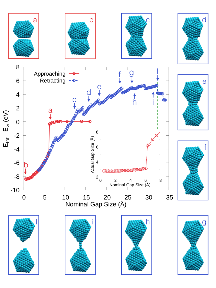
The total energy of the system during this process of approaching and retracting is shown as a function of the nominal gap size in Fig. 1. The evolution of the clusters and junction geometry is shown in the panels of Fig. 1 for selected separation distances. The latin letters that label each panel relate the geometry of the system to the corresponding nominal gap size and energy, as indicated in the curves of the figure. During the approach (red circles) the total energy remains constant until a nominal gap size of about 7.5 is reached. From this separation, the total energy starts decreasing smoothly. At a nominal gap size of 6.1 the two clusters suddenly jump to contact. Pethica and Suttom (1988) At this point the actual interface distance abruptly decreases and the energy is substantially reduced. The clusters are now connected and elongated along the intermolecular axis. The inset in Fig. 1 shows the actual gap size indicating the real distance between the inner facets of the clusters. After the jump-to-contact, the value of the actual gap size drops to a value of about 3.2 remaining fairly constant and close to 3.0 as the two clusters get closer together. The abrupt reduction of the energy at the jump-to-contact point is mostly due to the reduction of the surface energy of both clusters (two facets disappear). However, this happens at the expense of a large elastic deformation of the clusters. By further approaching the two clusters we reduce the elastic deformation of the system and, correspondingly, the total energy decreases. Eventually the system suffers some reorganizations which are also reflected (although they are somewhat less obvious than the jump-to-contact) in the energy versus distance curve in Fig. 1. For example, the stacking of the atomic layers at the interface, initially imposed by the mirror symmetry of our starting geometry, gets optimized at a nominal gap size of approximately 2.5 . Later, the particles start to deform to try to reduce further their surface area by increasing the contact cross-section. The energy finally stabilizes and starts to slowly increase for nominal gap sizes below 1 . We stop our approaching process at this point.
Once the two clusters are clumped together at a nominal distance comparable to the interlayer distance in bulk sodium, we start pulling apart them (blue circles in Fig. 1). During the retraction process the whole structure evolves creating and thinning a neck that connects the two clusters until a monatomic chain is formed and, eventually, until a complete separation of the clusters is achieved (point l in Fig. 1). In agreement with previous studies, the evolution of the contact structure takes place via an alternation of elastic and plastic deformation events. Rubio et al. (1996); Torres and Sáenz (1996); Sánchez-Portal et al. (1997); Untiedt et al. (1997); Sørensen et al. (1998); Rubio-Bollinger et al. (2001); Jelínek et al. (2003); Agraït et al. (2003) The contact is elongated until the accumulated elastic energy is sufficient to produce atomic rearrangements, mainly driven by the atoms in the neck area. During these plastic events the energy of the system decreases abruptly. Thus, there is a one-to-one correspondence between the discontinuities of total energy in Fig. 1 and the changes in the configuration of the metal neck. It is striking to note the dramatic contrast between the distance at which the jump-to-contact takes place and the clusters “touch” for the first time during the approaching process (close to point a in Fig. 1), and the distance at which they finally detach (indicated by a vertical green dashed line). A nominal gap distance of 32.3 is needed to separate completely the clusters.
In summary we have seen that the geometry of the system strongly departs from the idealized situation in which two clusters simply change their relative position. These structural rearrangements had been overlooked by most previous studies of plasmonics although, as we describe in the following, they play a key role in determining the optical response of the cavity.
III Optical response of a forming plasmonic cavity: relaxed vs. unrelaxed cases
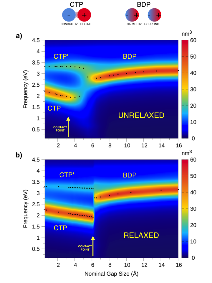
To explore the connection between the structural evolution and the plasmonic response of the cavity, we calculate the optical absorption of a plasmonic junction as the clusters approach for two situations: first, no relaxation of the clusters is allowed and the only parameter modified is the distance between the particles [Fig. 2 (a)]; second, the relaxation of the atoms is taken into account [Fig. 2 (b)] following the atomic-scale restructuring shown in Fig. 1 (red symbols). The resonant plasmonic modes of the forming cavity, as obtained from the calculated polarizability of the system, are displayed as a function of the inter-particle distance in both situations. The component of the polarizability parallel to the dimer axis is considered here, i.e., induced by an electrical field polarized along the same axis, that we take hereafter as z. In both cases, and depending on the separation, we can identify three distinct resonances. Pérez-González et al. (2010); Zuloaga et al. (2009); Esteban et al. (2012); Savage et al. (2012); Zhang et al. (2014); Esteban et al. (2015); Barbry et al. (2015) A single intense so-called Bonding Dipolar Plasmonic (BDP) resonance around 3 eV dominates the response at large inter-cluster distances when the two clusters interact weakly. The BDP shows an induced charge distribution characterized by a capacitive coupling of charges of opposite sign at both sides of the cavity, as schematically depicted in the right drawing of the top panel in Fig. 2. When both clusters are in contact, so that free charges can efficiently move across the junction, we enter a conductive coupling regime characterized by the so-called Charge Transfer Plasmon (CTP) and the associated high-energy Charge Transfer Plasmon (CTP’) modes. The conducting link of the CTP through the junction of the clusters, produces a screening of the charges in the cavity, and thus redistributes the induced charge density to produce a net dipole that extends to the whole dimer structure, as depicted in the top-left scheme in Fig. 2 [see also the panel c) and d) ].
The BDP resonance is redshifted as the inter-cluster distance is reduced and the Coulomb interactions among the clusters increase. This shift is due to the strong interaction of the parallel induced dipoles along the dimer axis, which hybridize Prodan et al. (2003) lowering the energy of the resulting optically active mode. In this capacitive (weak interaction) regime both unrelaxed and relaxed cases show the same dependence on the inter-particle distance. The BDP mode lives until the clusters are brought to a distance of about 6.1 . At this point, for the unrelaxed dimer [see Fig. 2 (a)], the BDP mode is quenched and higher energy modes start gaining intensity. If the clusters are approached further we observe a smooth transition from the capacitive to the conductive coupling regime. For separation distances right below 6 the electron tunnelling current at relevant frequencies gradually starts flowing, giving rise to the progressive emergence of the CTP resonance. Marinica et al. (2012); Esteban et al. (2012, 2015); Barbry et al. (2015) This transition region is frequently referred to as the quantum tunnelling regime of plasmonic cavities. Savage et al. (2012) At a distance comparable to the sodium interlayer distance, 3.0 , the clusters become chemically bonded and a clear contact is established. Under those conditions, a substantial current can be established and the CTP appears fully developed.
In contrast, the situation shown in Fig. 2(b) for the relaxed dimer is strikingly different. The relaxed dimer undergoes a jump-to-contact instability (see red curve in Fig. 1) that dramatically modifies the evolution of the optical spectrum. The transition regime, found between 6 and 3 for the unrelaxed dimer, has almost completely disappeared in the relaxed case. There are not stable geometries for those intermediate gap sizes and, thus, the resistive tunnelling (transition) regime cannot be clearly identified in the optical response in this case. Although the details of the jump-to-contact process strongly depend on the size and shape of the facets and the effective elastic constants of the systems being brought into contact, this effect is a quite general behavior which is routinely taken into account in the interpretation of data from scanning probe microscopies. Hofer et al. (2003) Our results indicate that the effect of the jump-to-contact must be considered when exploring and interpreting the optical response of metallic particles in close proximity, particularly when large atomic-scale reconfigurations can be expected. Importantly, this phenomenon can hinder the appearance of a smooth transition between the capacitive and charge-transfer regimes in the optical response of plasmonic cavities.
In panels (c) and (d) of Fig. 2 we explore the real space distribution of the induced charge for the CTP and CTP’ modes right after the clusters get into contact, i.e., right after the jump-to-contact instability. Here we plot the imaginary part of the induced density at the resonant frequencies. We also plot the corresponding electron current (graph to the right of each charge density plot) flowing through planes (i.e., perpendicular to the dimer axis) as function of , the coordinate along the dimer axis. Details of the method used to calculate the current can be found in the Supplemental Material. Sup The density charge associated with the CTP forms a dipolar pattern over the whole system having a single node placed at the center of the system. Thus, the charge accumulation does not take place in the cavity interfaces, but rather extends to the whole system. Correspondingly, the current associated with the CTP resonance has its maximum at the gap center. On the other hand, the CTP’ mode presents two dipolar patterns on each cluster with nodes of the induced density charge in the center of the system as well as in the middle of each cluster. The charge distribution in this case is somewhat similar to what one can expect for the BDP mode. However, the current reveals a key piece of information to rule out this interpretation. In the case of the CTP’ resonance the maxima of the current are found both in the center of the system as well as within each cluster. This is indeed confirming that there is charge transfer among both clusters also in this high energy mode. Thus, the observed induced density pattern is better interpreted as the second optically active mode of a metal rod.
Finally, below 2 nominal gap size the conductive coupling regime of the junction is fully developed in both the unrelaxed and relaxed cases, with the CTP and the CTP’ resonances converging to similar values of energy, around 2.25 eV and 3.3 eV, respectively. This underlines the fact that the details of atom rearrangements at the cluster interface might not be so important in the determination of the optical response once the two clusters are fully chemically bonded.
IV Optical response of a retracting plasmonic junction: Optics driven by individual atoms
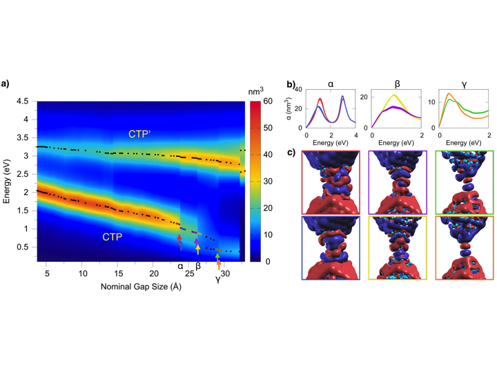
Fig. 3 shows the optical polarizability of the junction during the retraction process. Surprisingly, as the two clusters are retracted, the CTP and CTP’ modes dominate the spectrum for most separation distances, all the way to nominal inter-particle distances of several tens of Angstroms. This is in clear contrast with the results obtained in the previous section (approaching situation), and it is a result of the structural evolution of the junction, characterized by the formation of a thin conducting neck among the clusters [as shown in the panels (c)-(i) of Fig. 1]. As the clusters get separated, the neck gets longer and thinner. As a consequence, the charge transfer modes disperse towards lower energies (due to the overall elongation of the system). Moreover, as the neck cross-section is reduced, the intensity of the CTP’ mode increases at the expense of the lower-energy CTP resonance, consistent with calculations of stretched clusters. Rossi et al. (2015) As the current flowing across the neck diminishes, the CTP’ mode converges towards the BDP mode while the CTP mode tends to disappear.
While the polarizability of the approaching situation in Fig. 2 only shows a clear discontinuity associated with the jump-to-contact instability of the cavity, the retracting situation shows a completely different behavior as a function of the separation distance. During retraction the optical spectrum is characterized by the appearance of many discontinuities both in the spectral position and the intensity of the resonances. A careful inspection of Fig. 1 reveals that these discontinuities happen at exactly the same nominal distances where jumps in the total energy are detected. Some of the most visible jumps are highlighted with arrows of different colors and marked with Greek letters in Fig. 3 (a), and the corresponding polarizability is plotted in detail on the panels of Fig. 3 (b), which extracts the spectral lines from the contour plot in (a). Each panel shows spectra corresponding to distances before and after one of the jumps, identified in the contour plot of Fig. 3 (a) with the corresponding colored dots and arrows. Consecutive curves correspond to configurations in which the inter-particle distance is changed by 0.2 . In each panel there are several, almost indistinguishable, spectra of the same color. This highlights that noticeable changes in the spectrum are indeed linked to the plastic deformation events in the neck, and not to the small rearrangements during elastic deformation. At each jump we observe clear changes in the intensities, widths and positions of the resonance peaks. The jumps affect primarily the low energy resonance, CTP, although they are also visible in the CTP’ mode. They are owing to the atomic reorganization in the neck region and they are specially visible for distances above 20 due to the small cross-section of the neck. Remarkably, for such thin necks even single atom movements produce visible changes in the optical response of the system, clearly associated with the quantized nature of the conductance through the junction neck. The jump at 29.3 indicates the formation of a well-ordered monatomic neck, i.e., the clusters are connected by a single row of atoms. The formation of such structures has been observed for many metals, for example in the case of Au, for which these monatomic wires have even been visualized by electron microscopy Ohnishi et al. (1998); Yanson et al. (1998); Sørensen et al. (1998); Sánchez-Portal et al. (1999); Rubio-Bollinger et al. (2001); Rodrigues and Ugarte (2001); Koizumi et al. (2001); Kizuka (2008); Agraït et al. (2003).
The intensity of the CTP resonance suffers an abrupt decrease for a nominal gap size of around 23 , becoming broader between 27 and 29.3 . Afterwards, simultaneously to the monatomic neck formation, the CTP resonance gets sharper with a consequent regain in intensity. This evolution is due to a combination of several effects, the most important being the quantization of electron transport in the metal neck. Such quantization is a well-known effect due to the small cross-section of the contact, comparable to the electron wavelength. Datta (1995) As a result of the lateral confinement, the electronic energy levels in a thin metal nanowire or neck get quantized and, at a given energy, only a discrete number of bands (or “channels” using the standard terminology in quantum transport) can contribute to the electron transport. Thus, under a small, static bias, if the electron injection from the electrodes (in our case the clusters) is efficient and the neck structure is sufficiently long and ordered, we can expect each channel at the Fermi level to contribute to transport with a quantum of conductance , Datta (1995) with the Planck’s constant. In the presence of defects or strong scattering in the connections to the electrodes, the transmission probability of the channels gets reduced. Datta (1995)
With these ideas at hand, we can easily explain the observed behaviors. The abrupt jump in the intensity of the CTP peak around 23 ( jump) is caused by the sudden reduction of the neck’s cross-section, as can be clearly seen in Fig. 3 (c) and the inset of Fig. 4. As expected, the reduction of the cross-section reduces the number of conduction channels and, therefore, the electric current flowing through the junction (this is confirmed in Fig. 4, discussed later in detail). The resonance peak also shifts to slightly lower energies. The origin of the intensity jump at 27 ( jump) is also similar: a cross-section reduction that translates onto a sudden decrease of the current as can be seen in Figures 3 (c) and 4. After this jump at 27 , the neck develops into a less ordered structure, creating a region of high scattering that hampers the electron transport between the clusters. As a consequence the CTP resonance broadens. Finally, once the relatively defect-free monatomic wire is formed, the transport through the neck becomes completely ballistic, i.e. all the electron that are injected to the monatomic wire get across the junction, and the peak in the polarizability becomes more defined again.
These quantization effects can also be observed in the shape of the distributions of induced charge density as the neck evolves during retraction. In panels (c) of Fig. 3 the imaginary part of the induced density associated with the CTP mode is plotted for those configurations immediately before and after the , and jumps (indicated by the colored arrows in the polarizability plot). Although the density change has a quite complex distribution, it is possible to follow the evolution of the patterns towards simpler schemes of charge oscillation after each jump. The induced density presents a complex distribution and nodal structure, with a decreasing number of nodes as the cross-section of the neck gets thinner, a fact that reflects the larger number of open conduction channels for the wider structures. Subtle changes in the structure that have a direct translation in the optical response can also be observed in these density plots. For example, in the case of the jump, the three-atoms-long monatomic wire becomes more straight and the connections to the cluster more symmetric. This slightly increases the current flowing through the structure and produces the aforementioned changes in the plasmonic response.
Once the two clusters totally separate, breaking the neck, two split resonances arise near the CTP’ resonance at about 2.6 and 3.2 eV. The initial face-to-face configuration has been substituted by an asymmetric tip-to-tip configuration (see panel l in Figure 1). The lower energy resonance recalls a BDP mode, with the largest charge accumulations around the central gap (see the Supplemental Material Sup ). The higher energy resonance has a more complex charge distribution, corresponding to higher order mode, showing charge accumulations both in the tips inside the cavity and in the facets of the clusters (see the Supplemental Material Sup ).
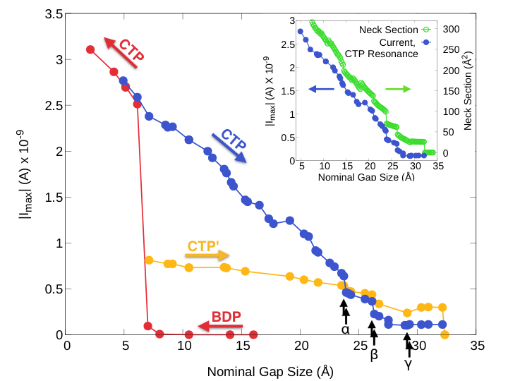
To fully account for the connection between high-frequency electron transport and optical response of the plasmonic junction, we have calculated the current through the junction as a function of the nominal gap size. In Figure 4 the results for the modulus of the current passing through a plane cutting the center of the junction are shown. Here we present the current computed at the frequencies of the main resonances of the polarizability, described in previous sections.
The current during the approach process is shown by red solid circles, corresponding first to the BDP mode, and later to the CTP mode, once the clusters are in contact. The current for the BDP mode is negligible until the jump-to-contact event takes place. Once the clusters are connected the current can flow through the whole system and therefore its value increases dramatically. The current calculated for the CTP resonance increases almost linearly as we decrease the nominal gap size.
The values of the current across the junction at the energies of the CTP and CTP’ resonances, while retracting the clusters and the neck is getting thinner, are plotted respectively in blue and yellow. The current related to the CTP resonance decreases monotonously as we elongate the system. As commented above, its evolution is characterized by abrupt jumps whenever the neck suffers a plastic deformation. The current eventually reaches a plateau associated with the formation of a well-defined monatomic neck. Interestingly, once the monatomic neck is formed, a further neck stretching does not affect considerably the current. This can be expected since the conductance of such small necks mostly depends on the cross-section, which is fixed for the monatomic wire. It is interesting to mention that for the low energy CTP mode, it was possible to define the conductance of the monatomic neck as the ratio of the current and the voltage drop across the wire. The modulus of the optical conductance (which is a complex number now) computed in this way at the CTP frequency is 0.65 , close to the expected value for a monatomic sodium wire at low frequency, . In this case it was possible to define the conductance without ambiguity since the potential drop is confined to the gap region, with the electrostatic potential flat inside the clusters. Sup For larger cross-sections of the necks and/or higher energies of the mode, this condition is not fulfilled and the definition of the conductance is quite involved. The current associated with the CTP’ mode follows the same trends than that of the CTP, although shows a less pronounced dependence on the overall elongation of the system. Obviously, once the clusters separate the current becomes negligible.
The arrows in Figure 4 indicate the position of the jumps shown in Figure 3 (a). Except for the last jump at 29.3 , the other two jumps observed in the polarizability (Fig. 3) and in the total energy (Fig. 1) show a clearly correlated sudden change in the current. This points towards a remarkable effect of a few atoms (or even a single atom), whose motion influences the overall optical response of the whole system (containing 760 atoms in our case). This observation can be of utmost importance in the control and manipulation of optical signal in subnanometric junctions which are clearly affected by this type of physical processes at the atomic scale.
To establish a more direct connection between the computed current as a function of the gap separation within the junction and the well-known quantization of transport in metal nanocontacts, in the inset panel of Fig. 4 we show the current for the CTP while retracting (left axis of the graph) plotted in relationship with the neck cross-section (right axis of the graph). As can be seen, there is an almost perfect correlation between the changes in the current and the evolution of the neck cross-section (see the Supplemental Material for the procedure adopted here to calculate the neck cross-section Sup ). Such correlation has been already well-established in the case of low-frequency driving-fields being applied to the necks. It has been observed in the formation of metal nanocontacts in Scanning Tunnelling Microscopy (STM) and break-junctions experiments, and corroborated by many calculations. Agraït et al. (2003) Our Fig. 4 goes one step beyond, establishing such correlation at optical frequencies. With this additional piece of information, we can now summarize the results described in this section by unambiguously establishing the following cause-effect relationships: plastic deformation of the neck during elongation cross-section reduction abrupt drop of the current decrease of the intensity of the CTP mode. This process is sometimes accompanied by small shifts of the position of the resonance peak. Finally, as mentioned above, more disordered structures translate into broader and dimmer CTP resonances.
V Conclusions
In summary, we have shown how atomic-scale structural reorganizations are crucial to determine the optical properties of plasmonic cavities. Besides the importance of jump-to-contact events, that can almost completely eliminate any signature of the plasmonic tunnelling regime, the effects are particularly dramatic when a metal nanocontact is formed across the cavity. This is due to the strong dependence of the plasmonic response of the system on the quantized current flowing through the connecting neck.
The mechanical response of atom-sized necks is characterized by sudden rearrangements of the atomic structure, which frequently involve just a few atoms in the thinner part of the contact. Since the electron transport through thin metal nanocontacts is quantized, the corresponding changes of the current flowing across the junction are necessarily discontinuous. Our calculations demonstrate that this common observation under small applied dc biases can be extrapolated to the optical frequencies of the plasmon resonances of the cavity, at least for the short ballistic contacts considered here. These jumps in the current translate onto abrupt changes in the plasmonic response of the system. Thus, the discontinuous evolution of the spectral position, width and intensity of the CTP mode observed in our simulations is a direct consequence of the transport quantization in the connecting neck.
The correlation is clearly demonstrated, showing that remarkably, Optics follows the atoms. This is absolutely important in the design of subnanometric-scale optical modulators that rely in slight changes of the optical response against tiny configurational modifications. In our case we have analyzed relatively small icosahedral sodium clusters, however, we expect to find a similar behavior for other materials suitable for electronic applications, such as gold.
The effect of a single atom in the optical properties of a nanoscopic object as the one reported here, which can be probably extended to somewhat larger objects, has important consequences in optical engineering, molecular electronics, and photochemistry, where the optical response can now be tailored by a few atoms.
Acknowledgements.
We acknowledge useful discussions with Andrei G. Borisov and Ruben Esteban regarding the role of electron transport in the determination of the optical properties of metal nanojunctions, and Dietrich Foerster regarding efficient TDDFT calculations. We acknowledge financial support from projects FIS2013-14481-P and MAT2013-46593-C6-2-P from MINECO. MB, PK, FM and DSP also acknowledge support from the ANR-ORGAVOLT project and the Eurorégion Aquitaine-Euskadi program. MB acknowledges support from the Departamento de Educación of the Basque Government through a PhD grant. PK acknowledges financial support from the Fellows Gipuzkoa program of the Gipuzkoako Foru Aldundia through the FEDER funding scheme of the European Union.References
- Ozbay (2006) E. Ozbay, Science 311, 189 (2006).
- Brongersma and Shalaev (2010) M. L. Brongersma and V. M. Shalaev, Science 328, 440−441 (2010).
- Ritchie (1957) R. H. Ritchie, Phys. Rev. 106, 874 (1957).
- Barnes et al. (2003) W. L. Barnes, A. Dereux, and E. T. W., Nature 424, 824 (2003).
- Pitarke et al. (2007) J. M. Pitarke, V. M. Silkin, E. V. Chulkov, and P. M. Echenique, Rep. Prog. Phys. 70, 1 (2007).
- Maier (2007) S. A. Maier, Plasmonics: Fundamentals and applications (Springer, 2007).
- Enoch and Bonod (2012) S. Enoch and N. Bonod, eds., Plasmonics. From Basics to Advanced Topics, Springer Series in Optical Sciences, Vol. 167 (Springer, 2012).
- Schuck et al. (2005) P. J. Schuck, D. P. Fromm, A. Sundaramurthy, G. S. Kino, and W. E. Moerner, Phys. Rev. Lett. 94, 017402 (2005).
- Alonso-González et al. (2012) P. Alonso-González, P. Albella, M. Schnell, J. Chen, F. Huth, A. García-Etxarri, F. Casanova, F. Golmar, L. Arzubiaga, L. E. Hueso, J. Aizpurua, and R. Hillenbrand, Nature Communications 3, 684 (2012).
- Morton et al. (2011) S. M. Morton, D. W. Silverstein, and L. Jensen, Chem. Rev. 111, 3962 (2011).
- Barbry et al. (2015) M. Barbry, P. Koval, F. Marchesin, R. Esteban, A. G. Borisov, J. Aizpurua, and D. Sánchez-Portal, Nano Letters 15, 3410 (2015).
- Steuwe et al. (2015) C. Steuwe, M. Erdelyi, G. Szekeres, M. Csete, J. J. Baumberg, S. Mahajan, and K. C. F., Nano Lett. 15, 3217 (2015).
- Mühlschlegel et al. (2015) P. Mühlschlegel, H.-J. Eisler, J. F. Martin, B. Hecht, and D. W. Pohl, Science 308, 1607 (2015).
- Pelton et al. (2008) M. Pelton, J. Aizpurua, and G. Bryant, Laser Photonics Rev. 2, 136 (2008).
- Jimenez de Aberasturi et al. (2015) D. Jimenez de Aberasturi, A. B. Serrano-Montes, and L. M. Liz-Marzán, Adv. Opt. Mater. 3, 602–617 (2015).
- Xu et al. (2000) H. Xu, J. Aizpurua, M. Käll, and P. Apell, Phys. Rev. E 62, 4318 (2000).
- Bouhelier et al. (2003) A. Bouhelier, M. Beversluis, A. Hartschuh, and L. Novotny, Phys. Rev. Lett. 90, 013903 (2003).
- Neubrech et al. (2008) F. Neubrech, A. Pucci, T. W. Cornelius, S. Karim, A. Garcia-Etxarri, and J. Aizpurua, Phys. Rev. Lett. 101, 157403 (2008).
- Jensen et al. (2008) L. Jensen, C. M. Aikens, and G. C. Schatz, Chem. Soc. Rev. 37, 1061 (2008).
- Sigle et al. (2013) D. O. Sigle, E. Perkins, J. J. Baumberg, and S. Mahajan, J. Phys. Chem. Lett. 4, 1449 (2013).
- Aroca (2013) R. F. Aroca, Phys. Chem. Chem. Phys. 15, 5355 (2013).
- Shiohara et al. (2014) A. Shiohara, Y. Wang, and Liz-Marzán, J. Photochem. Photobiol. C 21, 2–25 (2014).
- Hakonen et al. (2015) A. Hakonen, M. Svedendahl, R. Ogier, Z.-J. Yang, K. Lodewijks, R. Verre, T. Shegai, P. O. Andersson, and M. Käll, Nanoscale 7, 9405 (2015).
- Hirsch et al. (2003) L. R. Hirsch, R. J. Stafford, J. A. Bankson, S. R. Sershen, B. Rivera, R. E. Price, J. D. Hazle, N. J. Halas, and J. L. West, Proc. Natl. Acad. Sci. U.S.A. 100, 13549 (2003).
- Huang et al. (2008) X. Huang, P. K. Jain, I. H. El-Sayed, and M. A. El-Sayed, Lasers Med. Sci. 23, 217 (2008).
- Lal et al. (2008) S. Lal, S. E. Clare, and N. J. Halas, Acc. Chem. Res. 41, 1842 (2008).
- Atwater and Polman (2010) H. A. Atwater and A. Polman, Nature Materials 9, 205 (2010).
- Li et al. (2012) X. Li, W. C. H. Choy, L. Huo, F. Xie, W. E. I. Sha, B. Ding, X. Guo, Y. Li, J. Hou, J. You, and Y. Yang, Advanced Materials 24, 3046 (2012).
- Zhang et al. (2013a) W. Zhang, M. Saliba, S. D. Stranks, Y. Sun, X. Shi, U. Wiesner, and H. J. Snaith, Nano Letters 13, 4505 (2013a).
- Garcia-Etxarri et al. (2010) A. Garcia-Etxarri, J. Aizpurua, J. Molina-Aldareguia, R. Marcilla, J. A. Pomposo, and D. Mecerreyes, Front. Phys. Chin. 5, 330 (2010).
- Polavarapua and Liz-Marzán (2013) L. Polavarapua and L. M. Liz-Marzán, Phys. Chem. Chem. Phys. 15, 5288 (2013).
- Virk et al. (2014) M. Virk, K. Xiong, M. Svedendahl, M. Käll, and A. B. Dahlin, NanoLett. 14, 3544 (2014).
- Thacker et al. (2014) V. V. Thacker, L. O. Herrmann, D. O. Sigle, T. Zhang, T. Liedl, J. J. Baumberg, and U. F. Keys, Nature Comm. 5, 3448 (2014).
- Li et al. (2015) M. Li, S. K. Cushingab, and N. Wu, Analyst 140, 386 (2015).
- Rodrigo et al. (2015) D. Rodrigo, O. Limaj, D. Janner, D. Etezadi, F. J. García de Abajo, V. Pruneri, and H. Altug, Science 349, 165 (2015).
- Oldenburg et al. (1998) S. J. Oldenburg, R. D. Averitt, S. L. Westcott, and H. N. J., Chem. Phys. Letters 288, 243 (1998).
- Fan et al. (2010) J. A. Fan, C. Wu, K. Bao, J. Bao, R. Bardhan, N. J. Halas, V. N. Manoharan, P. Nordlander, G. Shvets, and F. Capasso, Science 328, 1135 (2010).
- La Porta et al. (2015) A. La Porta, A. Sánchez-Iglesias, T. Altantzis, S. Bals, M. Grzelczak, and L. M. Liz-Marzán, Nanoscale 7, 10377 (2015).
- Anderson (2000) M. S. Anderson, Appl. Phys. Lett. 76, 3130 (2000).
- Stöckle et al. (2000) R. M. Stöckle, Y. D. Suh, V. Deckert, and R. Zenobi, Chem. Phys. Lett. 318, 131 (2000).
- Anger et al. (2006) P. Anger, P. Bharadwaj, and L. Novotny, Phys. Rev. Lett. 96, 113002 (2006).
- Huber et al. (2009) A. J. Huber, A. Ziegler, T. Köck, and R. Hillenbrand, Nature Nanotechnology 4, 153 (2009).
- Bonnell et al. (2012) D. A. Bonnell, D. N. Basov, M. Bode, U. Diebold, S. V. Kalinin, V. Madhavan, L. Novotny, M. Salmeron, U. D. Schwarz, and P. S. Weiss, Rev. Mod. Phys. 84, 1343 (2012).
- Amenabar et al. (2013) I. Amenabar, S. Poly, W. Nuansing, E. H. Hubrich, A. A. Govyadinov, F. Huth, R. Krutokhvostov, L. Zhang, M. Knez, J. Heberle, A. M. Bittner, and R. Hillenbrand, Nature Communications 4, 2890 (2013).
- Zhang et al. (2013b) R. Zhang, Y. Zhang, Z. C. Dong, S. Jiang, C. Zhang, L. G. Chen, L. Zhang, Y. Liao, J. Aizpurua, Y. Luo, J. L. Yang, and J. G. Hou, Nature 498, 82 (2013b).
- Danckwerts and Novotny (2007) M. Danckwerts and L. Novotny, Phys. Rev. Lett. 98, 026104 (2007).
- Marinica et al. (2012) D. C. Marinica, A. K. Kazansky, P. Nordlander, J. Aizpurua, and A. G. Borisov, Nano Lett. 12, 1333 (2012).
- Luo et al. (2013) Y. Luo, A. I. Fernández-Domínguez, A. Wiener, S. A. Maier, and J. B. Pendry, Phys. Rev. Lett. 111, 093901 (2013).
- Zuloaga et al. (2009) J. Zuloaga, E. Prodan, and P. Nordlander, Nano Lett. 9, 887 (2009).
- Esteban et al. (2012) R. Esteban, A. G. Borisov, P. Nordlander, and J. Aizpurua, Nat Commun 3, 825 (2012).
- Savage et al. (2012) K. J. Savage, M. M. Hawkeye, R. Esteban, A. G. Borisov, J. Aizpurua, and J. J. Baumberg, Nature 491, 574 (2012).
- Ciracì et al. (2012) C. Ciracì, R. T. Hill, J. J. Mock, Y. Urzhumov, A. I. Fernández-Domínguez, S. A. Maier, J. B. Pendry, A. Chilkoti, and D. R. Smith, Science 337, 1072 (2012).
- Wiener et al. (2012) A. Wiener, H. Duan, M. Bosman, A. P. Horsfield, J. B. Pendry, J. K. B. Yang, S. A. Maier, and Fernández-Domínguez, Nano Letters 12, 3308 (2012).
- Stella et al. (2013) L. Stella, P. Zhang, F. J. García-Vidal, A. Rubio, and P. García-González, J. Phys. Chem. C 117, 8941 (2013).
- Zhang et al. (2014) P. Zhang, J. Feist, A. Rubio, P. García-González, and F. J. García-Vidal, Phys. Rev. B 90, 161407 (2014).
- Esteban et al. (2015) R. Esteban, A. Zugarramurdi, P. Zhang, P. Nordlander, F. J. García-Vidal, A. G. Borisov, and J. Aizpurua, Faraday Discuss. 178, 151 (2015).
- Zapata et al. (2015) M. Zapata, A. S. Camacho Beltrán, A. G. Borisov, and J. Aizpurua, Optics Express 23, 8134 (2015).
- Varas et al. (2015) A. Varas, P. García-González, F. J. García-Vidal, and A. Rubio, J. Phys. Chem. Lett. 6, 1891 (2015).
- Martin and Girard (1997) O. J. F. Martin and C. Girard, App. Phys. Lett. 70, 705 (1997).
- Li et al. (2003) K. Li, M. I. Stockman, and D. J. Bergman, Phys. Rev. Lett. 91, 227402 (2003).
- Wen et al. (2015) F. Wen, Y. Zhang, S. Gottheim, N. S. King, Y. Zhang, P. Nordlander, and N. J. Halas, ACS Nano 9, 6428 (2015).
- Rossi et al. (2015) T. P. Rossi, A. Zugarramurdi, M. Puska, and R. M. Nieminen, (2015), arXiv:1509.01140 .
- Agraït et al. (2003) N. Agraït, A. Levy-Yeyati, and J. M. van Ruitenbeek, Phys. Reps. 377, 81 (2003).
- Landman et al. (1990) U. Landman, W. D. Luedtke, N. A. Burnham, and R. J. Colton, Science 248, 454 (1990).
- Correia and García (1997) A. Correia and N. García, Phys. Rev. B 55, 6689 (1997).
- Kondo and Takayanagi (1997) Y. Kondo and K. Takayanagi, Phys. Rev. Lett. 79, 3455 (1997).
- Kizuka (1998) T. Kizuka, Phys. Rev. Lett. 81, 4448 (1998).
- Ohnishi et al. (1998) H. Ohnishi, Y. Kondo, and K. Takayanagi, Nature 395, 780 (1998).
- Yanson et al. (1998) A. I. Yanson, G. Rubio Bollinger, H. E. van den Brom, N. Agraït, and J. M. van Ruitenbeek, Nature 395, 783 (1998).
- Kondo and Takayanagi (2000) Y. Kondo and K. Takayanagi, Science 289, 606 (2000).
- Rodrigues et al. (2000) V. Rodrigues, T. Fuhrer, and D. Ugarte, Phys. Rev. Lett. 85, 4124 (2000).
- Stöffler et al. (2012) D. Stöffler, S. Fostner, P. Grütter, and R. Hoffmann-Vogel, Phys. Rev. B 85, 033404 (2012).
- Bhushan et al. (1995) B. Bhushan, J. N. Israelachvili, and U. Landman, Nature 374, 607 (1995).
- Landman et al. (1996) U. Landman, W. D. Luedtke, and J. Gao, Langmuir 12, 4514 (1996).
- Gimzewski and Möller (1987) J. K. Gimzewski and R. M. Möller, Physica B 36, 1284 (1987).
- Ferrer et al. (1988) J. Ferrer, A. Martín-Rodero, and F. Flores, Phys. Rev. B 38, 10113 (1988).
- García and Escapa (1989) N. García and L. Escapa, Appl. Phys. Lett. 54, 1418 (1989).
- Muller et al. (1992) C. J. Muller, J. M. van Ruitenbeek, and L. J. de Jongh, Phys. Rev. Lett. 69, 140 (1992).
- Todorov and Sutton (1993) T. N. Todorov and A. P. Sutton, Phys. Rev. Lett. 70, 2138 (1993).
- Agraït et al. (1993) N. Agraït, J. G. Rodrigo, and S. Vieira, Phys. Rev. B 47, 12345 (1993).
- Pascual et al. (1993) J. I. Pascual, J. Méndez, J. Gómez-Herrero, A. M. Baró, N. García, and V. T. Binh, Phys. Rev. Lett. 71, 1852 (1993).
- Olesen et al. (1994) L. Olesen, E. Laegsgaard, I. Stensgaard, F. Besenbacher, J. Schiøtz, P. Stoltze, K. W. Jacobsen, and J. K. Nørskov, Phys. Rev. Lett. 72, 2251 (1994).
- Torres and Sáenz (1996) J. A. Torres and J. J. Sáenz, Phys. Rev. Lett. 77, 2245 (1996).
- Ward et al. (2007) D. R. Ward, N. K. Grady, C. S. Levin, N. J. Halas, Y. Wu, P. Nordlander, and D. Natelson, Nano Lett. 7, 1396 (2007).
- Emboras et al. (2015) A. Emboras, , J. Niegemann, P. Ma, C. Haffner, M. Luisier, C. Hafner, T. Schimmel, and J. Leuthold, (2015), arXiv:1508.07748 .
- Koval et al. (2010a) P. Koval, D. Foerster, and O. Coulaud, J. Chem. Theory Comput. 6, 2654 (2010a).
- Koval et al. (2010b) P. Koval, D. Foerster, and O. Coulaud, Phys. Status Solidi B 247, 1841 (2010b).
- Foerster and Koval (2009) D. Foerster and P. Koval, J. Chem. Phys. 131, 044103 (2009).
- Sánchez-Portal et al. (1997) D. Sánchez-Portal, P. Ordejón, E. Artacho, and J. M. Soler, Int. J. of Quantum Chem. 65, 453 (1997).
- Soler et al. (2002) J. M. Soler, E. Artacho, J. D. Gale, A. García, J. Junquera, P. Ordejón, and D. Sánchez-Portal, J. Phys.: Condens. Matter 14, 2745 (2002).
- (91) See the Supplemental Material at [URL will be inserted by publisher] for detailed information on the computational methods, calculation of the currents at optical frequencies, definition of the nanocontact cross-sections and initial structure of our clusters.
- Pethica and Suttom (1988) J. B. Pethica and A. P. Suttom, J. Vac. Sci. Technol. A6, 2494 (1988).
- Lassiter et al. (2008) J. B. Lassiter, J. Aizpurua, L. I. Hernandez, D. W. Brandl, I. Romero, S. Lal, J. H. Hafner, P. Nordlander, and N. J. Halas, Nano Letters 8, 1212 (2008).
- Sørensen et al. (1998) M. R. Sørensen, M. Brandbyge, and K. W. Jacobsen, Phys. Rev. B 57, 3283 (1998).
- Jelínek et al. (2003) P. Jelínek, R. Pérez, J. Ortega, and F. Flores, Phys. Rev. B 68, 085403 (2003).
- Rubio et al. (1996) G. Rubio, N. Agraït, and S. Vieira, Phys. Rev. Lett. 76, 2302 (1996).
- Sánchez-Portal et al. (1997) D. Sánchez-Portal, C. Untiedt, J. M. Soler, J. J. Sáenz, and N. Agraït, Phys. Rev. Lett. 79, 4198 (1997).
- Untiedt et al. (1997) C. Untiedt, G. Rubio, S. Vieira, and N. Agraït, Phys. Rev. B 56, 2154 (1997).
- Rubio-Bollinger et al. (2001) G. Rubio-Bollinger, S. R. Bahn, N. Agraït, K. W. Jacobsen, and S. Vieira, Phys. Rev. Lett. 87, 026101 (2001).
- Pérez-González et al. (2010) O. Pérez-González, N. Zabala, A. G. Borisov, N. J. Halas, P. Nordlander, and J. Aizpurua, Nano Lett. 10, 3090 (2010).
- Prodan et al. (2003) C. Prodan, E. C. Radloff, N. J. Halas, and P. Nordlander, Science 302, 419 (2003).
- Hofer et al. (2003) W. A. Hofer, A. S. Foster, and A. L. Shluger, Rev. Mod. Phys. 75, 1287 (2003).
- Sánchez-Portal et al. (1999) D. Sánchez-Portal, E. Artacho, J. Junquera, P. Ordejón, A. García, and J. M. Soler, Phys. Rev. Lett. 83, 3884 (1999).
- Rodrigues and Ugarte (2001) V. Rodrigues and D. Ugarte, Phys. Rev. B 63, 073405 (2001).
- Koizumi et al. (2001) H. Koizumi, Y. Oshima, Y. Kondo, and K. Takayanagi, Ultramicroscopy 88, 17 (2001).
- Kizuka (2008) T. Kizuka, Phys. Rev. B 77, 155401 (2008).
- Datta (1995) S. Datta, Electronic Transport in Mesoscopic Systems (Cambridge University Press, 1995).