Physical Architecture for a Universal Topological Quantum Computer
based on a Network of Majorana Nanowires
Abstract
The idea of topological quantum computation (TQC) is to store and manipulate quantum information in an intrinsically fault-tolerant manner by utilizing the physics of topologically ordered phases of matter. Currently, one of the most promising platforms for a topological qubit is in terms of Majorana fermion zero modes (MZMs) in spin-orbit coupled superconducting nanowires. However, the topologically robust operations that are possible with MZMs can be efficiently simulated on a classical computer and are therefore not sufficient for realizing a universal gate set for TQC. Here, we show that an array of coupled semiconductor-superconductor nanowires with MZM edge states can be used to realize a more sophisticated type of non-Abelian defect: a genon in an Ising Ising topological state. This leads to a possible implementation of the missing topologically protected phase gate and thus universal TQC based on semiconductor-superconductor nanowire technology. We provide detailed numerical estimates of the relevant energy scales, which we show to lie within accessible ranges.
Introduction
The promise of topological quantum computation (TQC) is to encode and manipulate quantum information using topological qubits Kitaev (2003); Freedman et al. (2002); Nayak et al. (2008). The quantum states of a topological qubit do not couple to any local operators, forming a non-local Hilbert space, and are therefore intrinsically robust to decoherence. Currently, one of the most promising avenues towards developing a topological qubit is in terms of Majorana fermion zero modes (MZMs) in spin-orbit coupled superconducting nanowires Read and Green (2000); Kitaev (2001); Sau et al. (2010a); Lutchyn et al. (2010); Alicea (2012); Beenakker (2013); Mourik et al. (2012); Das et al. (2012); Rokhinson et al. (2012); Deng et al. (2012); Churchill et al. (2013); Nadj-Perge et al. (2014); Chang et al. (2015).
Topologically protected qubits are most useful if the information stored in them can be controlled in a topologically protected way. A system of topological qubits that are in a rich enough topological phase to allow complete manipulation of the state space would lead to the construction of a universal topological quantum computer. Unfortunately, most of the topological phases that appear within experimental reach such as topological superconductors hosting MZMs Alicea (2012), the Pfaffian fractional quantum Hall (FQH) states Nayak et al. (2008), surface codes Fowler et al. (2012); L.B. et al. (2002); Ioffe and Feigel’man (2002); Douçot et al. (2003); Albuquerque et al. (2008); You et al. (2010); Xu and Fu (2010); Terhal et al. (2012); Vijay et al. (2015) and even the recently proposed parafermion zero modesBarkeshli and Qi (2012); You and Wen (2012); Clarke et al. (2013); Lindner et al. (2012); Cheng (2012); Barkeshli et al. (2013) are not complex enough to span the entire topological state space in a topologically protected way. In fact, the topologically protected unitary operations that are possible with MZMs correspond to the Clifford group, which can be efficiently simulated on a classical computer Gottesman (1999). Consequently, proposals for utilizing MZMs in quantum computation require non-topological operations, and perhaps interfacing them with conventional, non-topological qubits Bravyi (2006); Bonderson et al. (2010a); Sau et al. (2010b); Bonderson and Lutchyn (2011); Jiang et al. (2011).
Despite much previous work, it remains a major open problem to find a viable path towards universal TQC. Ref. Bravyi and Kitaev, 2000 showed that some 2D systems harboring MZMs could support universal TQC given the possibility of dynamical topology changes. However, proposals to exploit these ideas using topological superconductors in semiconductor-superconductor heterostructures Bonderson et al. (2010b), or the Moore-Read Pfaffian FQH state with tilted interferometry Freedman et al. (2006), were since found to be insufficient even in principle, as they lack a crucial ingredient: the existence of a finite energy quasiparticle excitation with an appropriate value of topological spin Bonderson et al. (2013). Other previously proposed physical platforms require either (1) exotic non-Abelian fractional quantum Hall (FQH) states, such as those which possess Fibonacci quasiparticles, or the Read-Rezayi FQH state Read and Rezayi (1999); Freedman et al. (2002); Bonesteel et al. (2005); Mong et al. (2014); Vaezi (2014); Cui and Wang (2015); Levaillant et al. (2015), or (2) complex designer Hamiltonians based on Josephson junction arrays, which effectively realize non-Abelian discrete gauge theories Kitaev (2003); Mochon (2003); Douçot et al. (2004); Cui et al. (2015). However, the viability of these proposals, even in principle, is questionable due to the difficulty of establishing the existence of non-Abelian FQH states and the impractically low energy scales of previously proposed designer Hamiltonians Albuquerque et al. (2008). Moreover, the scientific and technological advances required to realize such proposals are not directly relevant to those being developed in the pursuit of MZMs in spin-orbit coupled superconducting nanowires.
In this paper, we show that a network of coupled superconducting nanowires hosting MZMs can be used to realize a more powerful type of non-Abelian defect: a genon Barkeshli et al. (2013); Barkeshli and Qi (2012); Barkeshli and Wen (2010) in an Ising Ising topological state. The braiding of such genons can be shown to mathematically map onto the required dynamical topology changes of Ref. Bravyi and Kitaev, 2000 and therefore provides the missing topological single-qubit phase gate Barkeshli et al. (2013). Combined with joint fermion parity measurements of MZMs, these operations provide a way to realize universal TQC Bravyi and Kitaev (2002).
Our proposal consists of the following basic building blocks. First, we show that an array of suitably coupled MZMs in nanowire systems can realize a two-dimensional phase of matter with Ising topological order 111The Ising topologically ordered phase is topologically distinct from a topological (e.g. p + ip) superconductor, as the latter does not have intrinsic topological order Bonderson and Nayak (2013). The proposal of Kells et al. (2014) is thus insufficient for this purpose.. We do this by showing how to engineer an effective Kitaev honeycomb spin model in a realistic physical system of coupled Majorana nanowires, where each effective spin degree of freedom corresponds to a pair of Majorana nanowires. We present two approaches to doing this, corresponding to whether capacitive charging energies or Josephson couplings are the dominant energy scales. An analysis of the energy scales of a physically realistic system indicates that the Ising topological order could have energy gaps on the order of a few percent of the charging energy of the Josephson junctions of the system; given present-day materials and technology, and the constraints on the required parameter regimes, we estimate the possibility of energy gaps of up to several Kelvin.
Second, we show how short overpasses between neighboring chains, which are feasible with current nanofabrication technology, can be used to create two effectively independent Ising phases, referred to as an Ising Ising state. Changing the connectivity of the network by creating a lattice dislocation allows the creation of a genon; this effectively realizes a twist defect that couples the two layers together. Finally, the genons can be effectively braided with minimal to no physical movement of them, by tuning the effective interactions between them.
Realizing the Kitaev Model
We begin by providing a physical realization of a Kitaev model Kitaev (2006), which can be described by the following Hamiltonian with spin-1/2 degrees of freedom on each site of a brick lattice 222A rotation about on every other site takes (1) to the more conventional Kitaev form:
| (1) |
where for are taken to be the Pauli matrices. We take the unit cell of the brick lattice to be two vertically separated neighboring spins; is a sum over each two-spin unit cell and refers to the top-most spin within the unit cell.
is most naturally solved by expressing the spins in terms of Majorana operators as , together with a gauge constraint Kitaev (2006). can thus be rewritten as
| (2) |
where we have made use of the gauge constraint in writing the term. The gauge constraint allows us to separate the Majoranas into a set of gauge fields and , which commute with , together with Majorana modes that couple to these gauge fields. The non-Abelian Ising phase corresponds to the regime where forms a topological superconductor, such that the vortices of localize MZMs. Since the vortices are deconfined finite-energy excitations in the Ising phase, their topological twist is well-defined and can be exploited for a topologically protected phase gate.
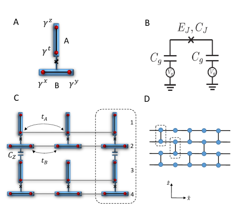
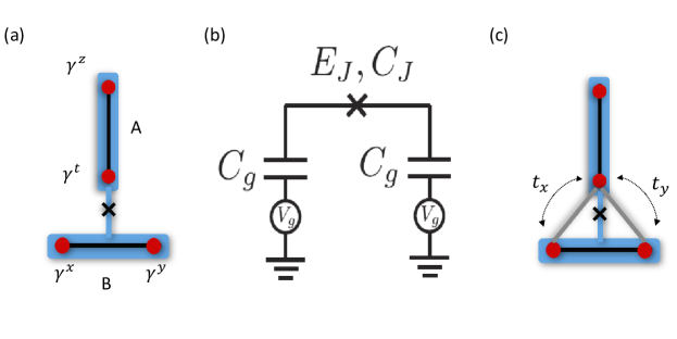
The Majorana solution of suggests that it might be physically realizable in a system where each spin is represented using a pair of proximity-induced superconducting nanowires with four MZMs , as shown in Fig. 1A. The semiconducting wires (such as InAs or InSb wires) can be either grown Krogstrup et al. (2015) or lithographically defined on 2D systems Shabani et al. (2015), and the superconductor thin films (such as Al, and perhaps other superconductors such as Nb and NbTiN) can now be epitaxially grown with exceptional interface qualities Krogstrup et al. (2015); Chang et al. (2015)Shabani et al. (2015).” As we show below, such a physical realization of is indeed possible; we first provide a proposal that physically implements the effective spins using the physics of charging energies, and subsequently we provide a second proposal which utilizes quantum phase slips.
In our first proposal (see Fig. 1), an overall charging energy for the pair of islands, each of which is controlled by a capacitance to a gate placed at a voltage , is used to effectively generate the gauge constraint by constraining the total charge of the pair of islands. For the four MZMs from each nanowire pair to be coherent with each other (in a sense which will be made more precise below), it is necessary to retain some phase coherence between the neighboring islands that comprise a single effective spin. This is obtained by connecting the islands and with a Josephson junction, with Josephson coupling and capacitance .
The effective Hamiltonian describing the Majorana and phase degrees of freedom for the system in Fig. 1(A) can be written as
| (3) |
Here is the BdG Hamiltonian for the nanowire on the th island, where is the proximity-induced superconducting gap on the th nanowire (at zero magnetic field). is the excess charge on the th superconducting island - nanowire combination. represents the number of Cooper pairs on the th superconducting island, is the total number of electrons on the th nanowire, and is the remaining offset charge on the th island, which can be tuned continuously with the gate voltage . The capacitance matrix is given by , for .
In order to decouple the fermions in from the phase fluctuations , we perform a unitary transformation : , with
| (4) |
where we have defined , , , , , and . For wires in the topological superconducting phase, at energies below the single particle gap , creates essentially decoupled Majorana zero modes which affect the phase dynamics only through the occupation numbers , . In order to allow the MZMs to remain free except for a constraint on the total fermion parity, we consider tuning the gate voltages so that , where is an integer, and . The ground state of the system is then two-fold degenerate, with , , and . There is an energy gap on the order of to violating the gauge constraint by changing the total charge of the system, and, for , a gap of order to excited states of that are related to fluctuations of the relative phase .
For energy scales below , the system can therefore be described as an effective spin-1/2 system, with . Tuning slightly away from zero acts like a Zeeman field for this effective spin degree of freedom, giving an effective Hamiltonian , with . This is equivalent to tunneling terms between the Majorana modes and . Effective Zeeman fields , can also be induced by allowing electrons to tunnel between the MZMs , and , (see Supplemental Materials). We emphasize that the MZMs are not exactly equivalent to the used in Eq. 2, because the two effective spin states in this setup differ not only in the Majorana occupation numbers , but also in the wave function of (see Supplemental Material). We can think of as corresponding to , dressed with the degrees of freedom.
The next step is to generate the quartic Majorana couplings in Eq. 2 by coupling the different island pairs together. For example, the term in Eq. 2 essentially represents a coupling between the occupation numbers and of neighboring SC islands in the lattice and can be realized using a capacitor . This is shown in Fig. 1(C), where we have also introduced the labelling for the vertically coupled islands. For numerical optimization of energy scales, it is useful to also consider a capacitance between islands and , which is not shown explicitly in Fig. 1.
To estimate the resulting coupling, we consider a detailed model for two vertically coupled effective spins, consisting of four vertically separated islands (see Fig. 1C), which is described by a Hamiltonian
| (5) |
and are the Hamiltonians for the isolated units of the form of Eq. 14, while capacitively couples the two effective spins. As expected couples the differences of the charges on the islands. are related to the four-island capacitance matrix (see Supplemental Materials).
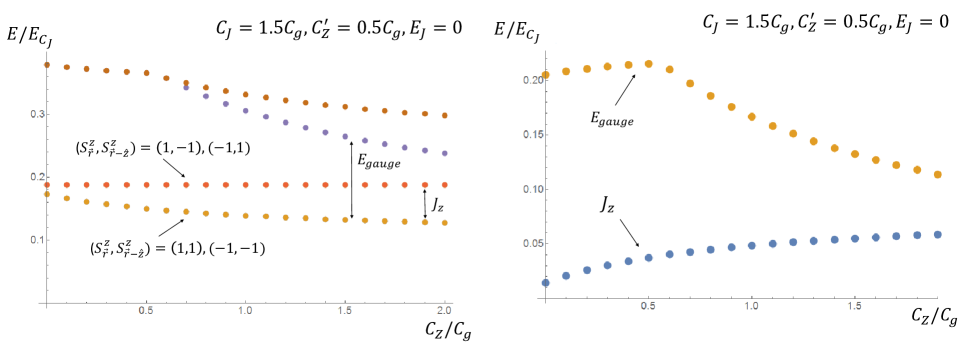
The term in Eq. 5 generates a coupling between the effective spins and by coupling the charges on the various islands. For small coupling capacitances , this can be estimated perturbatively. The limits of validity of the perturbative estimate can be checked by a direct numerical calculation of the spectrum of , which we have performed and presented in the Supplemental Material. An example of a suitable parameter regime is for , , and . In this case, we find , while the gap to all other states in the system is . Thus the gauge constraint is implemented effectively through a large energy penalty , and the system is well-described at low energies by the effective spin model (or, equivalently, the constrained Majorana model).
The terms in Eq. 2 involve coupling MZMs in the horizontal direction. This quartic Majorana coupling can be obtained from single electron tunneling processes between the MZMs through (normal) semiconductor wires that run horizontally, as shown in Fig. 1C. The electron tunneling amplitudes and can also be controlled with a gate voltage. The resulting Hamiltonian for the full 2D system shown in Fig. 1C,D is then
| (6) |
where is the Hamiltonian for the two-spin unit cell at , given by (5) above. The single electron tunnelings , violate the gauge constraint, which is related to fermion parity of the single effective spin, and thus induce an energy penalty on the order of . We consider the limit where , so that can be treated perturbatively around the decoupled unit cell limit. Assuming further that , , where is the single-particle gap on the th superconducting nanowire, we can replace , after the unitary transformation , by the MZMs:
| (7) |
where we have set after the unitary transformation , the c-number is the wave function of the MZM, and , are the fermion parities of the and islands of site . It is useful to define , , so that after the unitary transformation by , . Treating perturbatively around the decoupled unit cell limit, we obtain an effective Hamiltonian
| (8) |
are constants that depend on parameters of the model, in particular the angle . For and , we find . Therefore, up to negligible corrections, we arrive at the effective Hamiltonian (1) above, with . Physically, the angle can be tuned by the applied magnetic flux piercing the loop defined by the tunneling paths and also the angle between the Zeeman field and the Rashba splitting of the wire.
In the Supplemental Materials we provide detailed numerical estimates for the parameters of the effective spin model. For the parameter choice , , described above, and , we find that , , , and thus . Combined with the above estimate , we see that the energy scales are on the order of a few percent of the charging energy of the Josephson junctions. For Al-InAs-Al Josephson junctions, one can achieveDoh et al. (2005) , implying that would have energy scales on the order of several hundred milli-Kelvin. Nb-InAs-Nb Josephson junctions would in principle be able to support energy scales on the order of 7-8 times larger, with on the order of several Kelvin, due the correspondingly larger superconducting gap of Nb.
The phase diagram of Eq. (1)-(2) contains two phases Kitaev (2006): a phase where the fermions form a trivial insulating phase when , and a phase where the fermions are gapless with a Dirac-like node when . Both phases have an Abelian topological sector associated with the gauge fields . It is possible to open a topological gap for the Dirac node, and thus realize the non-Abelian Ising phase, by breaking the effective time-reversal symmetry of (1) with a Zeeman field , the implementation of which was described above.
A potentially more optimal approach to inducing the non-Abelian Ising phase is to use a modified structure where each point of the brick lattice of Fig. 1 is expanded into three points, with the couplings as shown in Fig. 2 Yao and Kivelson (2007). The ground state on this lattice spontaneously breaks the effective time-reversal symmetry of (1) and gaps out the Dirac nodes in the regime where to open a topological gap on the order of .
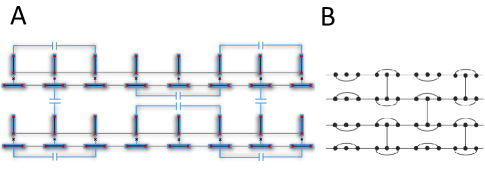
In our system, the small perturbations , can be used to controllably tune the sign of the spontaneous time-reversal symmetry breaking and thus control whether the system enters the Ising phase or its time-reversed conjugate, denoted .
Ising Ising phase and genons
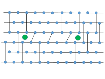
A crucial feature of the physical setup that we have proposed is that the vertical couplings between neighboring spins only involve capacitances (or Josephson junctions as described in the quantum phase slip based implementation below). This means that once a single copy of the model is realized, it is straightforward to realize two effectively independent copies of the model by creating short overpasses. Specifically, this can be done as shown in Fig. 3 by fabricating the superconducting wires that run in the vertical direction to pass over one pair of nanowires and to couple capacitively to the next chain over in the vertical direction.
The Ising phase contains three topologically distinct classes of quasiparticle excitations, labelled as , , and . The Ising Ising phase contains nine topologically distinct classes of quasiparticles, which we label as , for .
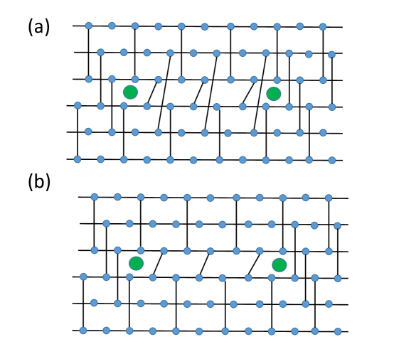
A genon, which we label in the Ising Ising phase is a defect in the capacitive couplings between vertically separated chains, associated with the endpoint of a branch cut that effectively glues the two copies to each other (see Fig. 3) 333Note that only half of a branch cut is sufficient, following Barkeshli and Qi (2014). A full branch cut would also contain vertical couplings that skip over two chains.. This defect in the lattice configuration of the superconducting islands is not a quasiparticle excitation of the system, but rather an extrinsically imposed defect with projective non-Abelian statistics Barkeshli et al. (2013, 2014) 444See Barkeshli and Wen (2010); Bombin (2010); Kitaev and Kong (2012); Barkeshli and Qi (2012); You and Wen (2012); Clarke et al. (2013); Lindner et al. (2012); Cheng (2012); Vaezi (2013)for other examples of twist defects in other topological states. has quantum dimension , and possesses the following fusion rules 555Technically, there are three topologically distinct types of genons Barkeshli et al. (2014), as can be bound to the quasiparticles, although this additional complication will be ignored in the present discussion.:
| (9) |
In Barkeshli et al. (2013), it was shown that the braiding of genons maps to Dehn twists of the Ising state on a high genus surface, which is known Bravyi and Kitaev (2000); Freedman et al. (2006) to provide a topologically protected phase gate. The protocol for implementing the phase gate using genon braiding was described in Barkeshli et al. (2013). In the present system, the braiding of genons is complicated by the fact that it is difficult to continuously modify the physical location of the genons to execute a braid loop in real space. Fortunately, this is not necessary, as the braiding of the genons can be implemented through a different interaction-based approach, without moving the genons, as described for general anyon systems in Bonderson (2013). To do this, we require that it be possible to project the joint fusion channel of any pair of genons into either the channel or the channel. This can be done by adiabatically tuning the effective interactions between the genons, similar to proposals for braiding MZMs in nanowire networks Alicea et al. (2010); Sau et al. (2011).
In order to implement the phase gate, we wish to start with two pairs of genons, labelled , and have the ability to braid genons and . To do this, we require an ancillary pair of genons, labelled and . The braiding process is then established by adiabatically changing the Hamiltonian of the system to effectively project the genons and onto the fusion channel , then the genons and onto the fusion channel , the genons and onto the fusion channel , and finally again the genons and onto the fusion channel (see Fig. 22).
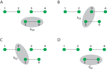
We will asssume here for simplicity that . If the genons and are created out of the vacuum, then it will in fact be natural to have . As long as , are Abelian, i.e. equal to either or , then the results of Barkeshli et al. (2013); Bonderson (2013) imply that the matrix obtained for a double braid (i.e. a full exchange), is given by
| (10) |
where is an undetermined, non-topological phase. In other words, the state obtains a relative phase of if the fusion channel is as compared with , or .
When two genons are separated by a finite distance , the effective Hamiltonian in the degenerate subspace spanned by the genons obtains non-local Wilson loop operators:
| (11) |
describes the exchange of a particle between the two genons, which equivalently corresponds to a or particle encircling the pair of genons. , for , are the tunneling amplitudes, with being the energy gap for the quasiparticles, and their velocity. When a quasiparticle encircles a topological charge , it acquires a phase , where is the modular matrix of the Ising phase Nayak et al. (2008). As we show in the Supplemental Materials, this implies that for our purposes, we only need to ensure that and, in the case where , we must have .
The tunneling amplitudes , can be tuned physically by tuning the parameters of the model, such as the electron tunneling amplitudes , , the capacitances , and the gate voltages . Therefore, to tune the interactions between two desired genons, we tune the parameters of the model in order to decrease the energy gap to the quasiparticle excitations along the path that connects them. A more detailed study of this will be left for future work.
We note that it is also possible to implement effectively the same physics by using instead the Ising state. In this case, the genons are replaced by holes with gapped boundaries, and the topological charge projections are implemented along various open lines that connect the different gapped boundaries. A detailed discussion of this variation is presented in the Supplemental Materials.
Quantum Phase Slip Limit
An alternative architecture is also possible, if we replace the purely capacitive coupling by a Josephson junction, with Josephson coupling and capacitance . In this case we consider the limit where the Josephson energies , are much larger than the charging energies , leading to a state with long range phase coherence. In the limit where the charging energies are ignored, the system has a large degeneracy due to the MZMs. A small charging energy induces quantum phase slips of the superconducting phase of the islands; the amplitude of the quantum phase slips depends on the occupation of the MZMs on the superconducting islands, thus inducing an effective Hamiltonian in the space of states spanned by the MZMs. The effective Hamiltonian takes the form: , where consists of single-island phase slips:
| (12) |
and consists of double island phase slips:
| (13) |
is the same as in Eqn. (Realizing the Kitaev Model) and describes electron tunneling in the horizontal direction. The single island phase slips are modulated by the offset charge: and can therefore be tuned to zero using the gate voltages. Double island phase slips that are not included in can be ignored in this limit, as can phase slips that involve more than two islands, as they are exponentially suppressed. We wish to choose parameters to operate in the limit . In this case, effectively imposes the gauge constraint for states with energies much less than . Each site can therefore be described by a spin-1/2 degree of freedom. The term involving acts like a coupling . As before, in this limit can be treated perturbatively, and gives rise to the desired coupling .
Acknowledgments
We thank Michael Freedman, Charlie Marcus, Chetan Nayak, Zhenghan Wang, Javad Shabani, Vladimir Manucharyan, Matthias Troyer, Roman Lutchyn, Meng Cheng, Parsa Bonderson for discussions. J. S. was supported by Microsoft Station Q, startup funds from the University of Maryland and NSF-JQI-PFC During the preparation of this manuscript we became aware of ongoing work that is related to the analysis of interaction-based braiding of genons in the Ising Ising state Lindner et al. (2015).
References
- Kitaev (2003) A. Kitaev, Annals Phys. 303, 2 (2003), eprint arXiv:quant-ph/9707021.
- Freedman et al. (2002) M. H. Freedman, M. Larsen, and Z. Wang, Communications in Mathematical Physics 227, 605 (2002), ISSN 0010-3616.
- Nayak et al. (2008) C. Nayak, S. H. Simon, A. Stern, M. Freedman, and S. D. Sarma, Rev. Mod. Phys. 80, 1083 (2008).
- Read and Green (2000) N. Read and D. Green, Phys. Rev. B 61, 10267 (2000).
- Kitaev (2001) A. Y. Kitaev, Physics-Uspekhi 44, 131 (2001).
- Sau et al. (2010a) J. D. Sau, R. M. Lutchyn, S. Tewari, and S. Das Sarma, Phys. Rev. Lett. 104, 040502 (2010a).
- Lutchyn et al. (2010) R. M. Lutchyn, J. D. Sau, and S. Das Sarma, Phys. Rev. Lett. 105, 077001 (2010).
- Alicea (2012) J. Alicea, Reports on Progress in Physics 75, 076501 (2012).
- Beenakker (2013) C. Beenakker, Annual Review of Condensed Matter Physics 4, 113 (2013).
- Mourik et al. (2012) V. Mourik, K. Zuo, S. Frolov, S. Plissard, E. Bakkers, and L. Kouwenhoven, Science 336, 1003 (2012).
- Das et al. (2012) A. Das, Y. Ronen, Y. Most, Y. Oreg, M. Heiblum, and H. Shtrikman, Nature Phys. 8, 887 (2012).
- Rokhinson et al. (2012) L. P. Rokhinson, X. Liu, and J. K. Furdyna, Nat. Phys. 8, 795 (2012), ISSN 1745-2473, eprint arXiv:1204.4212.
- Deng et al. (2012) M. T. Deng, C. L. Yu, G. Y. Huang, M. Larsson, P. Caroff, and H. Q. Xu, Nano Letters 12, 6414 (2012), eprint arXiv:1204.4130.
- Churchill et al. (2013) H. O. H. Churchill, V. Fatemi, K. Grove-Rasmussen, M. T. Deng, P. Caroff, H. Q. Xu, and C. M. Marcus, Phys. Rev. B 87, 241401 (2013).
- Nadj-Perge et al. (2014) S. Nadj-Perge, I. K. Drozdov, J. Li, H. Chen, S. Jeon, J. Seo, A. H. MacDonald, B. A. Bernevig, and A. Yazdani, Science 346, 602 (2014), eprint 1410.0682.
- Chang et al. (2015) W. Chang, S. M. Albrecht, T. S. Jespersen, F. Kuemmeth, P. Krogstrup, J. Nygård, and C. M. Marcus, Nat Nano 10, 232 (2015).
- Fowler et al. (2012) A. G. Fowler, M. Mariantoni, J. M. Martinis, and A. N. Cleland, Phys. Rev. A 86, 032324 (2012).
- L.B. et al. (2002) I. L.B., M. Feigel’man, A. Ioselevich, D. Ivanov, M. Troyer, and G. Blatter, Nature 415, 503 (2002).
- Ioffe and Feigel’man (2002) L. B. Ioffe and M. V. Feigel’man, Phys. Rev. B 66, 224503 (2002).
- Douçot et al. (2003) B. Douçot, M. V. Feigel’man, and L. B. Ioffe, Phys. Rev. Lett. 90, 107003 (2003).
- Albuquerque et al. (2008) A. F. Albuquerque, H. G. Katzgraber, M. Troyer, and G. Blatter, Phys. Rev. B 78, 014503 (2008).
- You et al. (2010) J. Q. You, X.-F. Shi, X. Hu, and F. Nori, Phys. Rev. B 81, 014505 (2010).
- Xu and Fu (2010) C. Xu and L. Fu, Phys. Rev. B 81, 134435 (2010).
- Terhal et al. (2012) B. M. Terhal, F. Hassler, and D. P. DiVincenzo, Phys. Rev. Lett. 108, 260504 (2012).
- Vijay et al. (2015) S. Vijay, T. Hsieh, and L. Fu (2015), eprint arXiv:1504.01724.
- Barkeshli and Qi (2012) M. Barkeshli and X.-L. Qi, Phys. Rev. X 2, 031013 (2012), eprint arXiv:1112.3311.
- You and Wen (2012) Y.-Z. You and X.-G. Wen, Phys. Rev. B 86, 161107 (2012).
- Clarke et al. (2013) D. J. Clarke, J. Alicea, and K. Shtengel, Nature Comm. 4, 1348 (2013), eprint arXiv:1204.5479.
- Lindner et al. (2012) N. H. Lindner, E. Berg, G. Refael, and A. Stern, Phys. Rev. X 2, 041002 (2012), eprint arXiv:1204.5733.
- Cheng (2012) M. Cheng, Phys. Rev. B 86, 195126 (2012), eprint arXiv:1204.6084.
- Barkeshli et al. (2013) M. Barkeshli, C.-M. Jian, and X.-L. Qi, Phys. Rev. B 87, 045130 (2013), eprint arXiv:1208.4834.
- Gottesman (1999) D. Gottesman, in Proceedings of the XXII International Colloquium on Group Theoretical Methods in Physics, edited by S. P. Corney, R. Delbourgo, and P. D. Jarvis (International Press, Cambridge, MA, 1999), eprint arXiv:quant-ph/9807006v1.
- Bravyi (2006) S. Bravyi, Phys. Rev. A 73, 042313 (2006).
- Bonderson et al. (2010a) P. Bonderson, D. J. Clarke, C. Nayak, and K. Shtengel, Phys. Rev. Lett. 104, 180505 (2010a).
- Sau et al. (2010b) J. D. Sau, S. Tewari, and S. Das Sarma, Phys. Rev. A 82, 052322 (2010b), URL http://link.aps.org/doi/10.1103/PhysRevA.82.052322.
- Bonderson and Lutchyn (2011) P. Bonderson and R. M. Lutchyn, Phys. Rev. Lett. 106, 130505 (2011).
- Jiang et al. (2011) L. Jiang, C. L. Kane, and J. Preskill, Phys. Rev. Lett. 106, 130504 (2011).
- Bravyi and Kitaev (2000) S. Bravyi and A. Y. Kitaev, unpublished (2000).
- Bonderson et al. (2010b) P. Bonderson, S. D. Sarma, M. Freedman, and C. Nayak (2010b), eprint arXiv:1003.2856.
- Freedman et al. (2006) M. Freedman, C. Nayak, and K. Walker, Phys. Rev. B 73 (2006).
- Bonderson et al. (2013) P. Bonderson, L. Fidkowski, M. Freedman, and K. Walker (2013), eprint arXiv:1306.2379.
- Read and Rezayi (1999) N. Read and E. Rezayi, Phys. Rev. B 59, 8084 (1999).
- Bonesteel et al. (2005) N. E. Bonesteel, L. Hormozi, G. Zikos, and S. H. Simon, Phys. Rev. Lett. 95, 140503 (2005), URL http://link.aps.org/doi/10.1103/PhysRevLett.95.140503.
- Mong et al. (2014) R. S. K. Mong, D. J. Clarke, J. Alicea, N. H. Lindner, P. Fendley, C. Nayak, Y. Oreg, A. Stern, E. Berg, K. Shtengel, et al., Phys. Rev. X 4, 011036 (2014), URL http://link.aps.org/doi/10.1103/PhysRevX.4.011036.
- Vaezi (2014) A. Vaezi, Phys. Rev. X 4, 031009 (2014).
- Cui and Wang (2015) S. X. Cui and Z. Wang, Journal of Mathematical Physics 56, 032202 (2015).
- Levaillant et al. (2015) C. Levaillant, B. Bauer, M. Freedman, Z. Wang, and P. Bonderson, Phys. Rev. A 92, 012301 (2015).
- Mochon (2003) C. Mochon, Phys. Rev. A 67, 022315 (2003), URL http://link.aps.org/doi/10.1103/PhysRevA.67.022315.
- Douçot et al. (2004) B. Douçot, L. B. Ioffe, and J. Vidal, Phys. Rev. B 69, 214501 (2004).
- Cui et al. (2015) S. Cui, S.-M. Hong, and Z. Wang, Quantum Information Processing 14, 2687 (2015), ISSN 1570-0755.
- Barkeshli and Wen (2010) M. Barkeshli and X.-G. Wen, Phys. Rev. B 81, 045323 (2010), eprint arXiv:0909.4882.
- Bravyi and Kitaev (2002) S. Bravyi and A. Kitaev, Ann. Phys. 298, 210 (2002).
- Kitaev (2006) A. Kitaev, Annals of Physics 321, 2 (2006).
- Krogstrup et al. (2015) P. Krogstrup, N. L. B. Ziino, W. Chang, S. M. Albrecht, M. H. Madsen, E. Johnson, J. Nygård, C. M. Marcus, and T. S. Jespersen, Nature Materials 14 (2015).
- Shabani et al. (2015) J. Shabani, M. Kjaergaard, H. J. Suominen, Y. Kim, F. Nichele, K. Pakrouski, T. Stankevic, R. M. Lutchyn, P. Krogstrup, R. Feidenhans, et al., to appear (2015).
- Doh et al. (2005) Y.-J. Doh, J. A. van Dam, A. L. Roest, E. P. A. M. Bakkers, L. P. Kouwenhoven, and S. De Franceschi, Science 309, 272 (2005), eprint http://www.sciencemag.org/content/309/5732/272.full.pdf.
- Yao and Kivelson (2007) H. Yao and S. A. Kivelson, Phys. Rev. Lett. 99, 247203 (2007).
- Barkeshli et al. (2014) M. Barkeshli, P. Bonderson, M. Cheng, and Z. Wang (2014), eprint arXiv:1410.4540.
- Bonderson (2013) P. Bonderson, Phys. Rev. B 87, 035113 (2013).
- Alicea et al. (2010) J. Alicea, Y. Oreg, G. Refael, F. von Oppen, and M. P. A. Fisher, Nature Physics 7, 412 (2010).
- Sau et al. (2011) J. D. Sau, D. J. Clarke, and S. Tewari, Physical Review B 84, 094505 (2011).
- Lindner et al. (2015) N. Lindner, E. Berg, and A. Stern, unpublished (2015).
- Koch et al. (2007) J. Koch, T. M. Yu, J. Gambetta, A. A. Houck, D. I. Schuster, J. Majer, A. Blais, M. H. Devoret, S. M. Girvin, and R. J. Schoelkopf, Phys. Rev. A 76, 042319 (2007).
- Abay et al. (2012) S. Abay, H. Nilsson, F. Wu, H. Xu, C. Wilson, and P. Delsing, Nano Letters 12, 5622 (2012), pMID: 23030250, eprint http://dx.doi.org/10.1021/nl302740f.
- Günel et al. (2012) H. Y. Günel, I. E. Batov, H. Hardtdegen, K. Sladek, A. Winden, K. Weis, G. Panaitov, D. Grützmacher, and T. Schäpers, Journal of Applied Physics 112, 034316 (2012).
- Chua and Fiete (2011) V. Chua and G. A. Fiete, Phys. Rev. B 84, 195129 (2011).
- Barkeshli and Qi (2014) M. Barkeshli and X.-L. Qi, Phys. Rev. X 4, 041035 (2014), URL http://link.aps.org/doi/10.1103/PhysRevX.4.041035.
- Bonderson and Nayak (2013) P. Bonderson and C. Nayak, Phys. Rev. B 87, 195451 (2013).
- Kells et al. (2014) G. Kells, V. Lahtinen, and J. Vala, Phys. Rev. B 89, 075122 (2014).
- Bombin (2010) H. Bombin, Phys. Rev. Lett. 105, 030403 (2010), eprint arXiv:1004.1838.
- Kitaev and Kong (2012) A. Kitaev and L. Kong, Comm. Math. Phys. 313, 351 (2012).
- Vaezi (2013) A. Vaezi, Phys. Rev. B 87, 035132 (2013).
Appendix A Supplemental Material
Appendix B Charging Energy Based Implementation
We begin by describing an implementation where charging energies are the dominant energies in the system. We proceed by incrementally increasing the complexity of our analysis, by first describing the physics of a single effective spin, then two vertically coupled spins that will form the unit cell of the Kitaev model, and subsequently the horizontal couplings that will link all of the two-spin unit cells into the full effective spin model.
B.1 Single spin
Let us consider the configuration shown in Fig. 5(a), which consists of two superconducting islands, labelled and , each of which is proximity coupled to a Majorana nanowire. Each superconducting island is separated by a capacitance to a gate voltage . The and islands are coupled together through a Josephson junction, with Josephson coupling and junction capacitance . The effective Hamiltonian for this system is
| (14) |
Here, for is the superconducting phase on the and islands, is the BdG Hamiltonian for the nanowire on the th island, where is the proximity-induced superconducting gap on the th nanowire at zero magnetic field. is the excess charge on the th superconducting island - nanowire combination; it can be written as:
| (15) |
where represents the number of Cooper pairs on the th superconducting island, is the total number of electrons on the th nanowire, and is the remaining offset charge on the th island, which can be tuned continuously with the gate voltage .
The capacitance matrix is given by
| (16) |
The charging energy term can be rewritten in terms of the total and relative charges on the and islands:
| (17) |
where we have defined
| (18) |
The BdG Hamiltonian for the nanowire is given by
| (19) |
where . Here we have taken to be the coordinate along the wire and is the length of the wire. is the Rasha spin-orbit coupling, is the chemical potential, and is the effective mass of the electrons in the nanowire, is the magnetic field and is the Zeeman energy.
It is now useful to perform a unitary transformation in order to decouple the phase from the fermions in . Here, is the occupation number of the pair of Majorana zero modes on wire . It is given in terms of the Majorana zero modes as
| (20) |
Under this transformation, the charge transforms as:
| (21) |
Thus, taking , we obtain
| (22) |
Here, we have defined the combinations:
| (23) |
With this definition,
| (24) |
It is also useful to define
| (25) |
With these definitions, we see that the compactification of is:
| (26) |
While and are formally decoupled in the Hamiltonian, they are coupled through their boundary conditions. The ground state of can now be written as
| (27) |
Here, is the state of the Majorana zero modes, and is the state for the phase degrees of freedom. Importantly, the wave function of itself does depend on the values of , . Since the Hamiltonians for and are decoupled, we can immediately write the ground state wave function for :
| (28) |
where is the ground state wave function for , which is peaked at . Importantly, because of the compactification conditions on , we see that if is integer (half-integer), then must be periodic (antiperiodic) in .
For energies much less than the single-particle gap on the nanowire, we can ignore the excited single particle states associated with , and we can describe the system by the following effective Hamiltonian:
| (29) |
Let us define
| (30) |
We see that the effect of is to fix the total charge on the pair of , islands to a fixed value, and gives an energy cost of to increase the charge by one unit. If we set
| (31) |
then the ground state of the system will be given by
| (32) |
Therefore the system will have two lowest energy states, associated with . Thus we can define an effective spin degree of freedom:
| (33) |
We will denote these two states as :
| (34) |
where we have chosen for simplicity. Note that differ both in the value of and also the wave function . For future reference, it will also be useful to define the state
| (35) |
which has the opposite wave function as compared with .
The effective Hamiltonian in the two-dimensional space is given (up to an overall constant) by
| (36) |
The value of depends on parameters in , as described below.
B.1.1 Numerical Solution
The Hamiltonian (see Eqn. (B.1)). The three terms, , , commute with each other and can be separately solved. As discussed above, is gapped for energies below , aside from the zero energy states arising from the Majorana zero modes, while has a gap of . It is useful to solve numerically, for the different Majorana occupation numbers.
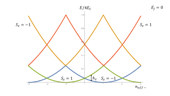
In Fig. 6 and Fig. 7, we plot the energy spectra for the four lowest energy states of , as a function of the offset charge , for the two different values of the Majorana occupation numbers . To connect with some standard notation in the literature for the well-known Hamiltonian , it will be useful to define
| (37) |
We see that for energies much smaller than , the system simply consists of the two states . These are degenerate when , and acquire a small splitting when .
B.1.2 Analytical Solution
The Hamiltonian can also be fully solved analytically through the use of Mathieu functions (see, e.g., Ref. Koch et al., 2007). Here we will provide this solution for reference. We find that
| (38) |
where is Mathieu’s characteristic value, and
| (39) |
| (40) |
int rounds to the nearest integer. The average charge on the island is given by:
| (41) |
Evaluating the partial derivative:
| (42) |
where
| (43) |
Note we have assumed that , which is true except for certain fine-tuned values of .
B.1.3 Effective and terms
Above we showed that tuning away from zero effectively acts like a Zeeman field in the direction. Zeeman fields in the and direction can also be generated, by allowing electron tunneling, with amplitude and , through the semiconducting wires as shown in Fig. 5c. Consider the following electron tunneling perturbations to :
| (44) |
After the unitary transformation , changes:
| (45) |
where
| (46) |
where
| (47) |
are the fermion parities of the and islands, respectively. Assuming the regime
| (48) |
where is the single-particle gap in the semiconducting nanowire, we can write the electron operators at low energies in terms of the Majorana zero modes:
| (49) |
where , and are complex numbers (whose magnitude is order unity) that depend on microscopic details. Thus, we obtain:
| (50) |
Recall that , and that , , which implies htat
| (51) |
It is useful to define
| (52) |
Thus, we get
| (53) |
where we have also commuted , through the exponential term. Note further that . The above can then be rewritten as
| (54) |
Thus, we have
| (55) |
with
| (56) |
For , we can treat perturbatively around . Thus, we get an effective Hamiltonian , such that
| (57) |
where are the normalized eigenstates of the unperturbed Hamiltonian . Then we can write the effective Hamiltonian in the low energy spin space as
| (58) |
where
| (59) |
B.2 Two spin unit cell
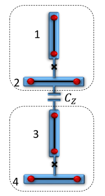
Let us now consider a pair of vertically separated effective spins, which will form the unit cell for our brick lattice Kitaev model. This consists of two pairs of and islands, as shown in Fig. 8. We wish to consider a capacitive coupling , as shown in Fig. 8. In this analysis we will label the islands as shown. We will also consider a capacitance , purely for subsequent numerical optimization of energy scales, between islands and , though this is not explicitly shown in Fig. 8. The Hamiltonian for such a two-spin system is given by
| (62) |
The charges (after the unitary tranformation discussed in the previous subsection) are
| (63) |
Note we omit the primed superscripts in the preceding equation and throughout the rest of the discussion. The capacitance matrix is now a matrix:
| (64) |
It is useful to write as
| (65) |
where
| (66) |
where we have defined and
| (67) |
The terms and are just the Hamiltonians for a single effective spin, which was analyzed in the previous section. We label these spins by and . and label the two different effective sites, as shown in Fig. 8. , then, couples the two effective spins.
B.2.1 Analytical treatment
We now wish to treat perturbatively around the decoupled limit . This is valid if
| (68) |
To lowest order in perturbation theory, we can replace with the effective Hamiltonian :
| (69) |
where we have defined (see eq. B.1.2)
| (70) |
The second equality in eq. (B.2.1) follows because , so only the term remains non-zero. We have assumed for simplicity that the two , island pairs have the same parameters , , .
Therefore, to first order in perturbation theory, the effect of the vertical capacitances , , which couple the two spins at and , is to induce an coupling.
B.2.2 Numerical Solution
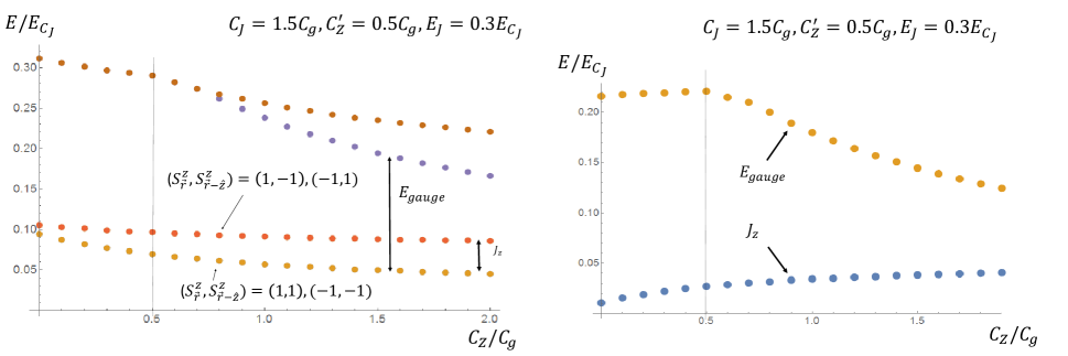
We can also more comprehensively analyze the two-spin model by employing a numerical solution. In Fig. 9 - 11, we present results of such a numerical solution for certain choices of parameters.


B.3 Horizontally coupled unit cells: four spins
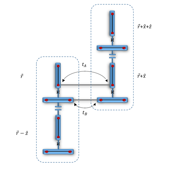
Let us now consider horizontally coupling two unit cells, as shown in Fig. 13. We connect two horizontally separated unit cells with semiconductor wire, as shown, which allows electrons to tunnel between the end points of the wires, with tunneling amplitudes and , as shown. The effective Hamiltonian for this system is now
| (71) |
where is the Hamiltonian for the th unit cell, which is given by above. contains the horizontal couplings, as we explain below.
We wish to show that in a suitable parameter regime, at low energies the effective Hamiltonian can be described by the following spin model:
| (72) |
with corrections to this effective Hamiltonian being much smaller in energy scale than .
We consider the electron tunneling terms and , as shown in Fig 13. This gives rise to an effective tunneling Hamiltonian (written in the basis before the unitary transformation ):
| (73) |
Here, labels the effective spins, each of which consists of an and a island. After the unitary transformation by , we have
| (74) |
where
| (75) |
where depending on whether or . Therefore, the tunneling Hamiltonian is, after the unitary transformation:
| (76) |
We consider the limit where
| (77) |
where is the single-particle gap in the nanowire. In this limit, the electron operator can be replaced by
| (78) |
where are complex numbers that depend sensitively on microscopic details. Let us also define
| (79) |
We therefore write as
| (80) |
These single electron tunneling processes violate the charging energy constraint and are therefore suppressed in the limit
| (81) |
where is the energy cost to adding a single electron to the two-spin unit cell. Perturbing in , we obtain an effective Hamiltonian:
| (82) |
Expanding, we obtain, up to a constant term,
| (83) |
| (84) |
| (85) |
| (86) |
Note that in the limit within which we are working,
| (87) |
Thus, due to the charging energy on each site , is highly fluctuating independently on each site. Treating (83) perturbatively around the decoupled limit , we see that we can set
| (88) |
| (89) |
Moreover, we can replace ,, by their expectation values in the ground state manifold of :
| (90) |
| (91) |
We define
| (92) |
Note that the phase depends on two quantities: the magnetic flux normal to the system, and the angle between the Zeeman field and the Rashba spin-orbit field. These can both be tuned, and therefore can be viewed as a tunable quantity.
| (93) |
The eigenstates of interest can be labelled as
| (94) |
Thus, we are interested in the matrix elements:
| (95) |
We see that the only non-zero matrix elements are those for which , , , and . Thus, we need to compute
| (96) |
In terms of these matrix elements, we can then write the effective Hamiltonian:
| (97) |
where
| (98) |
| (99) |
Now, simplifying , we get:
| (100) |
Here we have defined
| (101) |
The states with the tildes over the ’s indicate that the phase mode has the opposite wave function as compared with the spin degree of freedom, as described for the single spin case in Eq. (35). Let us define
| (102) |
In terms of , we have
| (103) |
We see that we need to compute the following expectation values for the two-spin system:
| (104) |
In terms of these expectation values,
| (105) |
Note that the eigenstates can be changed by a phase, which will modify the expressions above. It is useful to pick a choice of phase so that, when possible, .
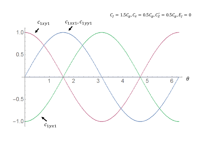
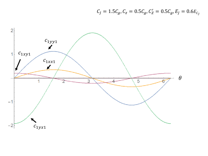
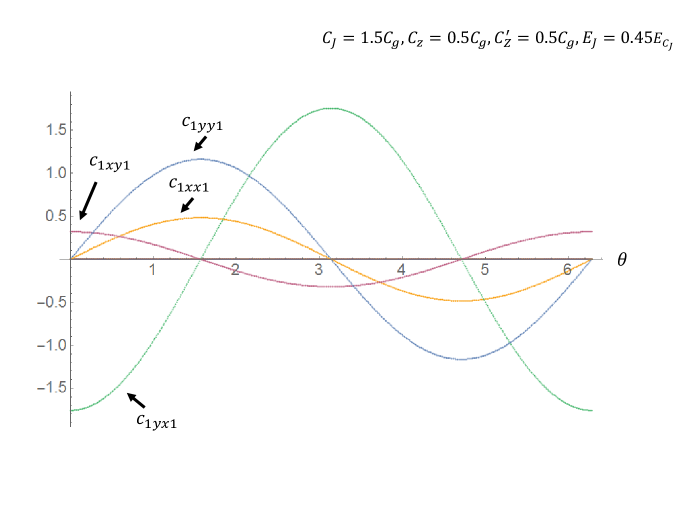
In Figs. 14-16, we display some results for the numerical calculation of . We see that in all cases, the only appreciable couplings are ; and are both quite small. This is because the amplitudes have a very weak dependence on and and thus essentially cancel each other in the sum.
When , then Fig. 14 shows that at , only ; for all values of , at least two of the four couplings , , , and are of the same order. As shown in Figs. 15-16, when , we can enter the regime where only is appreciable while all others are much smaller. In fact, we see from the equations above that if the matrix element is close to one, which is the case for large , then the only appreciable term in will be . This is the reason that we need to include . The optimal point would be to take to be as large as possible; however this would dramatically reduce the coupling, which was calculated in the previous section. Therefore, we need to find an optimal point where is non-zero so that only is appreciable, while is still large enough.
B.4 2D
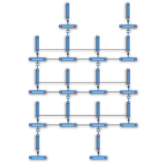
Let us now consider the 2D network shown in Fig. 17 . The effective Hamiltonian for this is given by
| (106) |
where is the Hamiltonian for the th unit cell; for each unit cell, this is given by above. contains the horizontal tunneling terms, which were analyzed for the case of two horizontally coupled unit cells in the preceding section. For the full 2D system, it is given by:
| (107) |
Perturbing around the independent unit cell limit , a simple generalization of the analysis of the preceding section gives the following effective Hamiltonian, which operates in the subspace spanned by the two effective spin states on each site:
| (108) |
where sums over all unit cells, and refers to the top spin of each two-spin unit cell. As we have shown in the preceding sections, there exist parameter regimes where the additional terms in are negligible:
| (109) |
can be recognized to be the Kitaev honeycomb spin model.Kitaev (2006) Specifically, one can perform a spin rotation around on every other site, which brings the into the form
| (110) |
which is the more familiar form of the Kitaev model. Here, .
B.5 Numerical Estimates of Energy Scales
In Figs. 6-16, we have presented the results of several numerical calculations of the energy spectra of the single effective spin, the two spin unit cell, and the couplings constants of the effective spin interaction terms. From Figs. 9 - 12, we see that the interactions, which couple the vertically separated spins via an interaction , must be on the order of a few percent of the Josephson charging energy , in order for the low energy spin manifold to be comfortably separated from the rest of the excitations of the system. Figs. 14 – 16 show that a finite Josephson coupling is required, so that the horizontal couplings will be in the appropriate regime of the Kitaev honeycomb model.
While we have not performed an exhaustive optimization, our preliminary calculations suggest that the following parameter regime is a good one:
| (111) |
With this choice of parameters, we find that , while the energy cost to the other excited states of the two-spin unit cell is approximately ten times as large, . This gives a comfortable energy window that separates the low-lying effective spin states and the rest of the states of the sytsem. Fig. 16 shows that with this choice of parameters, , while , and , as are all other horizontal coupling terms. This gives almost a factor of approximately 6 between the horizontal couplings that we want and the undesired ones. In terms of absolute energy scales, we have:
| (112) |
If we set to ensure the single electron tunneling processes are suppressed relative to the second order process, we find , which is almost the same order as the estimate above.
Therefore, we see that to get an effective spin model whose dominant interactions are the Kitaev interactions, while all other interactions are suppressed, we can get energy scales that are roughly in the range of a few percent of the Josephson charging energies . To get a large energy scale, then, we wish to use a physical setup with the largest possible Josephson charging energy , which can also simultaneously accommodate a Josephson coupling .
Typical Al-AlxO1-x Josephson junctions have Josephson charging energies on the order of , which can therefore give interaction strengths .
Josephson junctions made from gated semiconductor wires, such as Al-InAs-Al junctions, can yield much larger Josephson charging energies, because the distance between the superconductors (ie the length of the nanowire junction) can be much larger. For example, let us consider InAs wires with radius and a distance between the Al superconductors. For nm and nm, critical supercurrents nA have been measured,Doh et al. (2005) which corresponds to K. If we consider nm and the superconductor consisting of a wire of Al epitaxially grown on the InAs nanowire with total radius nm, we can estimate . Taking for InAs, this implies a charging energy K. This can be further reduced by increasing the radius or decreasing .
Interestingly, devices with nm have also been fabricated, and have been reported to yield critical currents as high as nA, for InAs nanowires with radius nm.Abay et al. (2012) This corresponds to K. If we assume the parallel plate capacitor formula for a radius nm and nm, we would get K. However, it is not clear whether such a high supercurrent is due to unwanted parasitic effects that are introduced during the fabrication process.
To put this on a somewhat more theoretical footing, consider that the supercurrent is typically given by
| (113) |
where is the normal-state resistance of the junction, and is the superconducting gap. For a semiconducting wire with channels, this implies
| (114) |
where the conductance is per channel. For Al, with K, this implies that K
The above considerations, and in particular the experimental measurements, suggest that it could be possible, with Al-InAs-Al junctions, to get to a regime where K. This would then imply
| (115) |
Note that Nb is also a candidate material that can be used in these setups, instead of Al. Indeed, Nb-InAs-Nb Josephson junctions have been fabricated and measured.Günel et al. (2012) While the use of Nb presents certain technical obstacles for fabricating the required semiconductor-superconductor heterostructures, it has the advantage that the superconducting gap is much larger, K. This implies that the energy scales considered above will be a factor of larger if Nb is used instead and good contact can be made between the Nb and the InAs. So far such an enhancement in the critical supercurrent has not been observed due to contact quality, but there are no fundamental obstacles to improving this contact quality and thus achieving this factor of enhancement.
This would then suggest the theoretical possibility
| (116) |
Superconductors with even larger gaps, such as NbTiN, could potentially yield even larger energy scales.
Appendix C Quantum Phase Slip Based Implementation
C.1 Single spin
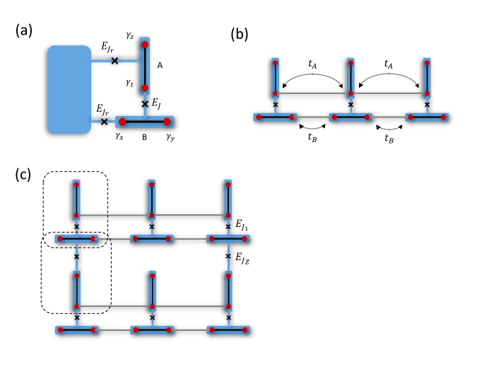
We now consider an alternative possible architecture, which utilizes the physics of quantum phase slips to engineer an effective Kitaev spin model. The main building block of this architecture is a set of four Majorana fermion zero modes, as shown in Fig. 18A. Each pair of Majorana zero modes arises from the endpoints of a spin-orbit coupled semiconductor nanowire, proximity coupled to a superconducting island. Each pair of Majorana fermion zero modes gives rise to two degenerate states, associated with whether the fermion parity on the island is even or odd. The four Majorana zero modes will be labelled as , , , and , as shown in Fig. 18A.
The effective Hamiltonian for the system shown in Fig. 18 A is
| (117) |
Here, for is the superconducting phase on the and islands, is the BdG Hamiltonian for the nanowire on the th island, where is the proximity-induced superconducting gap on the th nanowire at zero magnetic field. is the excess charge on the th superconducting island - nanowire combination; it can be written as:
| (118) |
where represents the number of Cooper pairs on the th superconducting island, is the total number of electrons on the th nanowire, and is the remaining offset charge on the th island, which can be tuned continuously with the gate voltage . The capacitance matrix is
| (119) |
As in Sec. B.1, we perform a unitary transformation in order to decouple the phase from the fermions in . Here, is the occupation number of the pair of Majorana zero modes on wire . It is given in terms of the Majorana zero modes as
| (120) |
Under this transformation, the charge transforms as:
| (121) |
Thus, taking , we obtain
| (122) |
where we have used , and we have set
| (123) |
In what follows we will drop the prime superscripts for convenience.
It is helpful to consider the Lagrangian for this system, which is given by
| (124) |
We consider the limit where
| (125) |
in which case , are pinned, while the conjugate variables , are highly fluctuating. For energy scales below , the effective Hamiltonian of this two island system takes the form
| (126) |
The first two terms are due to quantum phase slip events where either or change by . The last term is due to the quantum phase slip event where both islands and collectively change their phase by , relative to the phase of the reservoir. These phase slip processes effectively measure the fermion parity of the region undergoing the phase slip, which can be expressed in terms of the Majorana fermion modes.
The quantum phase slip amplitudes, , can be computed using the standard instanton calculation, in the limit of dilute instantons. To leading order in , we estimate this to be
| (127) |
where , and .
We assume that the direct coupling between these different Majorana zero modes, which is generated by electron tunneling between the two ends of the wires, is much smaller than all other energy scales in the problem, and can therefore be ignored.
Observe now that if we set
| (128) |
then the effective Hamiltonian is simply
| (129) |
which enforces the constraint
| (130) |
for states with energies much less than . The ground state subspace of this system is therefore doubly degenerate and acts like a spin, with
| (131) |
Slightly tuning the offset and/or away from acts like a Zeeman field .
C.2 1D Chain
Next, let us consider a 1D chain of the superconducting island pairs introduced in the previous subsection. The coupling between the effective sites of the chain consists of the Majorana fermion tunneling terms shown in Fig. 18B, with tunneling amplitudes and . In addition to the single particle tunneling terms between the Majorana zero modes, there are pair tunneling terms that induce Josephson couplings , between the islands. Finally, there are cross-capacitances between the different superconducting islands; we will consider the regime where the charging energies due to these cross-capacitances are much smaller than the tunneling and Josephson couplings, and can therefore be ignored. The effective Hamiltonian of the chain is therefore
| (132) |
where each is given by the Hamiltonian described in the previous section, and
| (133) |
Note that the pair tunnelings and in this setup are generated by pair tunneling between the Majorana zero modes, and thus , . Performing the unitary transformation in the previous section, and then setting
| (134) |
as in the previous section, we get:
| (135) |
Now, since we are in the limit of large Josephson couplings, all of the phases of the superconducting islands can be set equal to each other, which we can set to zero without loss of generality:
| (136) |
with corrections coming from instanton events. Thus, becomes
| (137) |
We wish to consider the limit where
| (138) |
In this case, the single tunneling events are suppressed; perturbing to second order in , we obtain an effective Hamiltonian:
| (139) |
Therefore, the effective Hamiltonian of the 1D chain is given by:
| (140) |
If we assume for simplicity that , then the quantum phase slip amplitudes are essentially as given in Eqn. C.3, with , and being twice the capacitance across the semiconductor wires.
C.3 2D Network
Now we would like to assemble the 1D chains described above into a two-dimensional network. We consider the network shown in Fig. 18C, which effectively forms a brick (honeycomb) lattice. Each unit cell of the lattice consists of two pairs of superconducting islands: two islands and two islands, separated vertically from each other. The Hamiltonian for the system can be written as
| (141) |
where is the location of the top spin of each unit cell, is thus a sum over unit cells, and the Hamiltonian for each unit cell :
| (142) |
The capacitance matrix now is
| (143) |
The tunneling Hamiltonian is:
| (144) |
We have ignored the capacitance between horizontally separated islands, as they are assumed to be far enough apart that their capacitance is negligible.
Based on the analysis of the single spin case and the 1D chain, we can now immediately see that the low energy effective Hamiltnian for this system can be written as
| (145) |
where consists of single island phase slips:
| (146) |
consists of two-island phase slips:
| (147) |
These phase slip amplitudes are given in terms of the Josephson couplings and charging energies:
| (148) |
| (149) |
where we have defined
| (150) |
The phase slip amplitudes , are approximately given by products of the single island phase slips,
| (151) |
because the horizontal Josephson couplings are negligible.
All other two-island phase slips, and collective phase slips of more than two islands, can be ignored, as their amplitudes are exponentially suppressed relative to the terms considered here. Finally, includes the Majorana tunneling terms and :
| (152) |
If we set , then the single island phase slips vanish. The effective Hamiltonian becomes
| (153) |
If we further consider the regime where
| (154) |
we see that the system can be described by an effective spin model:
| (155) |
with
| (156) |
Upon rotating every other spin around the axis by , the above Hamiltonian can be put into the more familiar Kitaev form:
| (157) |
Appendix D Realizing the Ising topological order
As we have shown, the physical architectures described above can give rise to an effective realization of the 2D Kitaev honeycomb spin model:
| (158) |
It is well-known that this model is proximate to a non-Abelian topological state with Ising topological order. There are a number of known ways to access the non-Abelian state. One way to access the non-Abelian state is to apply a small effective Zeeman field:
| (159) |
As explained in Sec. B.1, The term above can be generated by tuning the gate voltage on each of the superconducting islands. The and terms are more difficult, but possible, to generate as well. They require connecting the Majorana zero modes with additional semiconductor wires, as shown in Figs. 5c, to allow for electron tunneling as shown.
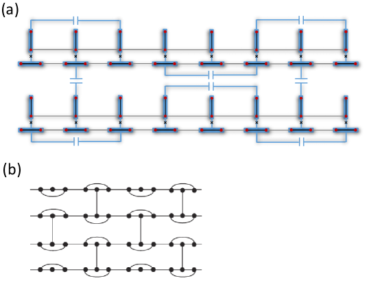
A second way of realizing the Ising topological order is to consider effectively the same model, but on a different lattice (see Fig. 19), as proposed by Yao and Kivelson. As a spin model, the Kitaev Hamiltonian, Eq. (158) is time-reversal invariant. On the lattice structure proposed by Yao-Kivelson the ground state spontaneously breaks time reversal symmetry, yielding a ground state with Ising (or its time-reversed partner, ) topological order. In the completely isotropic limit where all couplings are equal to , the energy gap of the Ising state is also equal to . Interestingly, disorder in the spin couplings can actually be beneficial and can enlarge the region of stability of the Ising phase.Chua and Fiete (2011)
By adding a small effective time-reversal symmetry breaking perturbation to the spin model, we can tune whether the topological order is Ising or , and avoid having domains of either, as would be realistically expected in the case where the effective time-reversal symmetry is broken spontaneously. A Zeeman term by itself is insufficient. We can consider either a Zeeman term that includes both and . Or, in order to avoid requiring or terms, which are more difficult to generate, we can make use of the smaller perturbations , , that are naturally generated in the first charging energy based implementation presented above.
Appendix E Genons
E.1 Ising Ising topological order
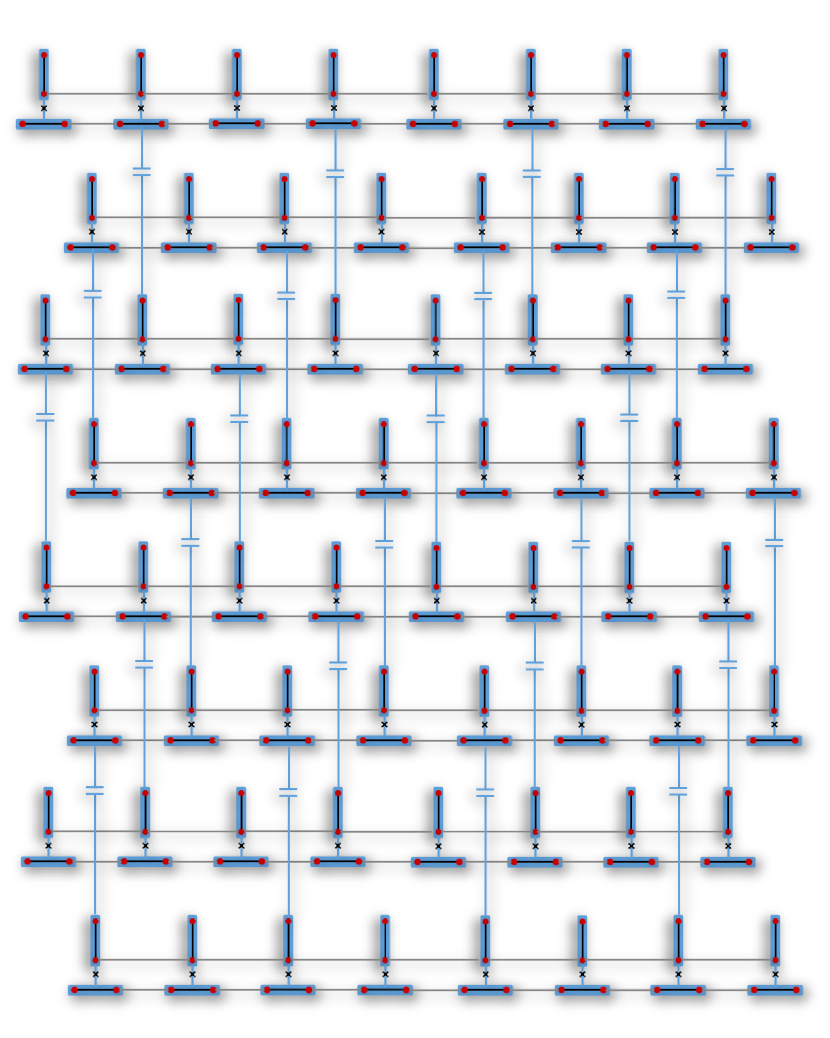
Given a microscopic architecture to realize a quantum state with Ising topological order, one can then consider designing two independent copies of such a state (referred to as the Ising Ising state) by utilizing present-day nanofabrication technology to create short overpasses among different superconducting wires, as shown in Fig. 20.
E.2 Creating genons
A genon in an Ising Ising state can then be realized by modifying the overpass connections to create a segment along which the connections among the horizontal chains is twisted, as shown in Fig. 21. These segments effectively create branch lines that connect one layer to the other, and vice versa. The end-points of the segments realize exotic non-Abelian twist defects, which have been referred to as genons. The topological degeneracy of the system in the presence of the genons mimics that of a single copy Ising system on a surface of non-trivial topology.Barkeshli and Wen (2010); Barkeshli and Qi (2012); Barkeshli et al. (2013)
Technically, there are three topologically distinct types of genons, which we label as , , and .Barkeshli et al. (2014) Physically, they correspond to whether a , , particle, from either layer, is bound to the genon. The genons have the following fusion rules:
| (160) |
It follows from the above that , have quantum dimension , while has quantum dimension .
E.3 Effective braiding of genons and the topological phase gate
In Ref. Barkeshli et al., 2013, it was shown that the braiding of genons can be used to realize a topologically protected phase gate. In the present system, the braiding of genons is complicated by the fact that it is difficult to continuously modify the physical location of the genons to execute a braid loop in real space. Fortunately, this is not necessary, as the braiding of the genons can be implemented through a measurement-based approach. To do this, we require that it be possible to measure the joint fusion channel of any pair of genons and project it into either the channel or the channel.
E.4 Measurement-based braiding of genons
Importantly, the braiding of the genons can be achieved without moving them continuously around each other in space, but rather through tuning the effective interactions between them. Specifically, what is required to braid two genons is the ability to project the fusion channel of pairs of genons onto an Abelian charge sector.
In order to implement the phase gate, we wish to start with two pairs of genons, labelled , and have the ability to braid genons and . In order to do this, we use an ancillary pair of genons, labelled and . The braiding process is then established by projecting the genons and onto the fusion channel , then the genons and onto the fusion channel , the genons and onto the fusion channel , and finally again the genons and onto the fusion channel .

We will asssume here that . If the genons and are created out of the vacuum, then it will in fact be natural to have . In this situation, we can derive the resulting braid matrix for the genons, following the results of Ref. Bonderson, 2013. When , the braid matrix for genons and is given by
| (161) |
where is an undetermined, non-topological phase. In other words, the state obtains a phase of or , depending on whether the fusion channel of genons and is , , or . If instead , then
| (162) |
E.5 Physical implementation of projection of pairs of genons onto or fusion channels
When two genons are separated by a distance , the effective Hamiltonian in the degenerate subspace spanned by the genons obtains non-local Wilson loop operators:
| (163) |
describes the exchange of a particle between the two genons, which equivalently corresponds to a or particle encircling the pair of genons. Similarly, describes the exchange of a particle between the two genons, which equivalently corresponds to a or particle encircling the pair of genons. and are the tunneling amplitudes, with and being the energy gaps for the and particles, and , some appropriate velocity scales.
Next, let us suppose that the pair of genons shown in the figure fuse to the quasiparticle . The outcome of the process where a quasiparticle encircles a topological charge is determined by the topological matrix of the Ising phase, and is given by , where
| (164) |
and where the entries are ordered . In other words, the eigenvalues of are given by , where is the fusion channel of the two genons connected by the path .
The ground state of , which depends on therefore corresponds to a definite fusion channel for the pair of genons involved. We can distinguish the following possibilities:
-
1.
and . The ground state subspace of corresponds to the case where the two genons have fused to the channel.
-
2.
and . The ground state subspace of corresponds to the case where the two genons have fused to the channel.
-
3.
, , . The ground state subspace of corresponds to the case where the two genons have fused to the channel.
-
4.
, , . The ground state subspace of corresponds to the case where the two genons have fused to the channel.
-
5.
, . The ground state subspace of corresponds to the case where the two genons have fused to the fusion channel.
We see that there is only one possibility that needs to be prevented, which is the last one, where , . To do this, we flip the sign of by flipping the sign of the coupling along a single link of the shortest path that connects the genons. Moreover, note that one can also pick the precise path along which the quasiparticles tunnel by depressing the gap along that path, which can be done by decreasing the couplings along that path.
E.6 Ising topological order and gapped boundaries
In the above, we have suggested creating genons in the Ising Ising topological state. The braiding of the genons, which can be performed in a measurement-based fashion, can be used for the topologically protected gate. Here we note that the same topologically robust transformations can also be achieved with the Ising topological state in the presence of multiple disconnected gapped boundaries, where refers to the time-reversed conjugate of the Ising state.
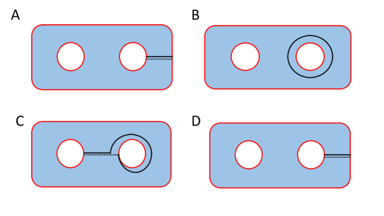
The main observation is that the Ising state in the presence of disconnected gapped boundaries can be viewed as effectively a flattened version of a single Ising state on a genus surface. This is similar to the fact that an Ising Ising state, in the presence of pairs of genons, can also be effectively mapped onto a single Ising state on a genus surface. The measurement-based braiding protocol for the genons of the Ising Ising state can be readily adapted to the case of the Ising with gapped boundaries. Below we will briefly sketch this adapted protocol, leaving a more detailed discussion for future work.
Let us consider the Ising state in the presence of two disconnected gapped boundaries, i.e. on an annulus. This is equivalent to a single Ising state on a torus, similar to the case of the Ising Ising state with four genons. In order to carry out an effective Dehn twist in this effective torus, we use an ancillary gapped boundary, as shown in Fig. 23. This system is now equivalent to a genus 2 surface. In order to effectively carry out the Dehn twist, we perform a series of projections along various loops in the system. We consider the loops shown in Fig. 23A-D, and sequentially project the topological charge through those loops to be . This is precisely analogous to the genon braiding case described in Fig. 22, where the fusion channel of genons was projected onto , , , and . Thus if we take and to be all Abelian topological charges, the equivalence between the Ising Ising system with genons and the Ising with gapped boundaries implies that we will have effectively carried out the desired operation.
As in the case of the genons in the Ising Ising state described in the previous sections, these projections can effectively be implemented by reducing the gap for quasiparticle tunneling along the various loops as required.