Structural, electronic, and optical properties of -plane InGaN/GaN quantum wells: Insights from experiment and atomistic theory
Abstract
In this paper we present a detailed analysis of the structural, electronic, and optical properties of an -plane (In,Ga)N/GaN quantum well structure grown by metal organic vapor phase epitaxy. The sample has been structurally characterized by x-ray diffraction, scanning transmission electron microscopy, and 3D atom probe tomography. The optical properties of the sample have been studied by photoluminescence (PL), time-resolved PL spectroscopy, and polarized PL excitation spectroscopy. The PL spectrum consisted of a very broad PL line with a high degree of optical linear polarization. To understand the optical properties we have performed atomistic tight-binding calculations, and based on our initial atom probe tomography data, the model includes the effects of strain and built-in field variations arising from random alloy fluctuations. Furthermore, we included Coulomb effects in the calculations. Our microscopic theoretical description reveals strong hole wave function localization effects due to random alloy fluctuations, resulting in strong variations in ground state energies and consequently the corresponding transition energies. This is consistent with the experimentally observed broad PL peak. Furthermore, when including Coulomb contributions in the calculations we find strong exciton localization effects which explain the form of the PL decay transients. Additionally, the theoretical results confirm the experimentally observed high degree of optical linear polarization. Overall, the theoretical data are in very good agreement with the experimental findings, highlighting the strong impact of the microscopic alloy structure on the optoelectronic properties of these systems.
pacs:
78.67.De, 73.22.Dj, 73.21.Fg, 77.65.Ly, 73.20.Fz, 71.35.-yI Introduction
(In,Ga)N/GaN quantum well (QW) structures grown on polar -plane substrates are the building blocks for nitride-based light emitters operating in the blue spectral region. Nakamura et al. (1993, 1994) However, when trying to push the emission wavelength into the green to yellow spectral region the device performance is hampered, among other factors, by the presence of strong electrostatic built-in fields, arising in part from the strain-dependent piezoelectric polarization and in part from the strain-independent spontaneous polarization. Bernardini et al. (1997) One consequence of the built-in field is the so-called quantum confined Stark effect (QCSE) which results in a shift of the emission to longer wavelength. Im et al. (1998); Leroux et al. (1998) Also the intrinsic field leads to a spatial separation of electron and hole wave functions, causing a reduced radiative recombination rate, Im et al. (1998); Fiorentini et al. (1999) an effect that can be particularly undesirable for high-efficiency optoelectronic devices. To circumvent these effects arising from the intrinsic built-in fields, which fundamentally are caused by the growth along the polar axis, significant research has been directed towards the fabrication of semi- and nonpolar structures. Waltereit et al. (2000); Kim et al. (2007); Schwarz and Kneissl (2007); Kappers et al. (2007); Gühne et al. (2008); Paskova (2008); Badcock et al. (2009); Schulz et al. (2010); Zhao et al. (2011); Seo et al. (2011); Pan et al. (2012); Scholz (2012); Matioli et al. (2012); Kundys et al. (2014); Sutherland et al. (2015) In the case of semi- and nonpolar planes the axis is at a nonvanishing angle with respect to the growth direction. In semipolar planes residual built-in fields are expected and observed, even though these fields are significantly reduced. Zhao et al. (2011); Scholz (2012) In terms of built-in field reduction, nonpolar QW systems are ideal since in these structures the -axis lies in the growth plane. Thus, in a perfect nonpolar system, there is no discontinuity in the built-in polarization vector field at the heterointerfaces, leading ideally to a field-free system. Waltereit et al. (2000); Schwarz and Kneissl (2007) Consequently, in such a structure the radiative recombination rate should be much higher than in polar QW structures. Additionally, (In,Ga)N QWs grown on nonpolar planes offer the possibility of acting as highly efficient sources of linearly polarized light, Gühne et al. (2008); Paskova (2008); Matioli et al. (2012) which may be of practical use in, e.g., back-lit liquid crystal displays. Paskova (2008) The potentially high degree of optical linear polarization (DOLP) in a nonpolar QW originates mainly from differences in the effective hole masses along the growth direction, which leads to a lifting of the degeneracy of the highest lying -like valence bands. Sun et al. (2003); Matioli et al. (2012)
However, the detailed consequences of random alloy fluctuations on the ideally zero built-in field and the optoelectronic properties of nonpolar systems have been largely ignored. Experimental studies on -plane (In,Ga)N/GaN QW systems reveal that random alloy fluctuations lead to carrier localization effects, which can dominate the electronic and optical properties of these structures. Wang et al. (2012); Hammersley et al. (2012) Clear experimental indications of the importance of alloy fluctuations on the properties of nonpolar (In,Ga)N QWs have also been presented. Sun et al. (2003); Seo et al. (2011); Sutherland et al. (2015) To fully understand the structural, electronic, and optical properties of nonpolar (In,Ga)N QWs requires the use of a range of advanced experimental and theoretical techniques. For example, 3D atom probe tomography (APT) can be used to help to identify whether the QW should be described by a clustered or random alloy. Galtrey et al. (2007); Tang et al. (2015a) This structural information can then form the basis of detailed theoretical modeling. However, from a theoretical viewpoint, polar and nonpolar (In,Ga)N QWs are widely treated as homogeneous systems described by average material parameters. Obviously, these approaches completely neglect wave function localization arising from effects that could be attributed to the microscopic alloy structure. Recently, continuum-based approaches have been modified to include random alloy fluctuations. Funato and Kawakami (2008); Watson-Parris et al. (2011); Yang et al. (2014) Even though such an approach captures some of the localization effects introduced by alloy fluctuations it cannot reveal the microscopic origin of localization effects, including in particular the presence of In-N-In-N chains as shown by density functional theory (DFT). Liu et al. (2010); Schulz et al. (2015a) Unfortunately, realistic QW systems cannot be treated in the framework of DFT due to the very large number of atoms () required in the calculations. Additionally, especially for nonpolar systems where the strong macroscopic electrostatic built-in field is absent, DFT calculations would have to be coupled with solving the Bethe-Salpeter equation or time-dependent DFT would have to be used to account for excitonic effects. These effects could be very important when comparing the results with photoluminescence (PL) measurements. Bester (2009) To be able to take all these factors into account, namely the large number of atoms, the atomistic description of the electronic structure, plus Coulomb correlation effects, semiempirical approaches, such as tight-binding Camacho Mojica and Niquet (2010); der Maur (2015); Schulz et al. (2015b) (TB) or empirical pseudopotential methods, Bester (2009); Molina-Sánchez et al. (2012) coupled with configuration interaction (CI) schemes, Franceschetti et al. (1999); Schulz et al. (2006); Bester (2009) are required.
In this work we combine advanced experimental and theoretical methods to analyze the structural, electronic and optical properties of nonpolar -plane (In,Ga)N/GaN QWs. Our approach allows us to clarify the impact of alloy fluctuations on the properties of nonpolar (In,Ga)N structures. We have conducted a comparative study of the predicted and measured optical properties of a 2 nm thick -plane (In,Ga)N/GaN QW structure grown on a freestanding GaN substrate. The heterostructure was grown by metal organic vapor phase epitaxy (MOVPE) and characterized by x-ray diffraction (XRD), scanning transmission electron microscopy (STEM), and 3D APT measurements. The detailed optical characterization of the sample was carried out by PL, polarized PL excitation (P-PLE) spectroscopy, and PL time decay measurements. The measured optical properties are compared with theoretical results. The theoretical framework is based on an atomistic TB model coupled with CI calculations to account for Coulomb effects. Our microscopic model takes input from experimentally determined structural properties and accounts for local strain and built-in field fluctuations arising from alloy fluctuations in the QW region.
The TB model assumes that the In atom distribution inside the QW is close to a random alloy, and we briefly discuss this assumption in the context of available APT data. The optical characterization reveals strong Stokes shifts and broad PL linewidth, which is indicative of strong carrier localization effects. Additionally, and in stark contrast to -plane systems, our time-resolved measurements exhibit decay transients that are single exponential. Also, we find in general an extremely high DOLP (). Using the experimentally obtained structural information as input for atomistic TB calculations we find very good agreement between theory and the optical spectroscopy measurements.
The theoretical analysis reveals strong hole wave function localization, which leads to a broad emission spectrum. When we include the Coulomb interaction between the electrons and holes in our calculations we find that electron wave functions localize about the hole wave functions, giving rise to localized excitons. This finding is consistent with the experimentally observed form of the decay transients. Also, the calculated PL transition energy is in good agreement with the experimentally measured value. Additionally, analyzing the wave function character of the valence band edge (VBE) shows a high DOLP similar to the experimental data. Overall, this combined experimental and theoretical analysis provides clear insights into the basic physical properties of -plane (In,Ga)N/GaN QWs.
The paper is organized as follows. The details of the growth of the sample are given in Sec. II. This is followed by the description of the applied structural characterization techniques, the results obtained, and how they are implemented in the theoretical framework (Sec. III). In Secs. IV.1 and IV.2 we describe the setup and the results of the experimental optical characterization of the -plane (In,Ga)N/GaN QWs, respectively. In Sec. IV.3 the ingredients of our theoretical framework are discussed, while Sec. IV.4 presents the theoretical results and the detailed comparison with the experimental data. Finally, we summarize our results in Sec. V.
II Sample Growth details
The -plane (In,Ga)N/GaN multiple-QW structure studied was grown by MOVPE in a Thomas Swan in close-coupled showerhead reactor on a freestanding -plane (1-100) GaN substrate. The misorientation of the substrate is in the negative direction. The substrate, provided by Ammono S. A., Kucharski et al. (2012) has a negligible basal plane stacking fault density and a threading dislocation density of 5 cm-2. Onto this freestanding substrate an initially undoped 2 m thick homoepitaxial GaN buffer layer was grown. For this growth step trimethylgallium (TMG) and ammonia (NH3), with H2 as the carrier gas, were used. A reactor pressure of 100 Torr at 1050∘C was applied. Subsequently five (In,Ga)N QWs were grown with a quasi-2T method, discussed in detail elsewhere. Pendlebury et al. (2007) For the QW growth a reactor pressure of 300 Torr was applied. TMG, trimethylindium (TMI), and NH3 have been used as precursors, with N2 as the carrier gas. The (In,Ga)N QWs were grown at a temperature of 735∘C. After the growth of each QW period a 1 nm GaN cap was grown at the (In,Ga)N growth temperature. The flows of TMG and NH3 were kept constant during the 90 s temperature ramp to 860∘C. After this 90 s temperature ramp the growth of the barrier material was completed.
III Structural Characterization: Setup, results and input into theoretical framework
Having presented growth details of the sample, we now turn to the analysis of its structural properties. In Sec. III.1 we briefly introduce the experimental techniques applied to analyze the structural properties of the -plane sample and the outcome of these studies. We discuss in Sec. III.2 how the experimental results serve as input for theoretical supercell (SC) structures, which underlie the atomistic calculations of the electronic and optical properties of the sample in question.
III.1 Structural characterization: Experimental setup and results
To analyze the structural properties of the -plane (In,Ga)N/GaN QW system, different techniques have been applied to obtain a comprehensive picture. The N QW and barrier widths as well as the In fraction () of the sample were determined by XRD. The sample was analyzed using a high-resolution x-ray diffraction MRD diffractometer from Panalytical equipped with a symmetric 4-bounce monochromator and a triple-axis analyzer to select the CuK1 wavelength. scans of the brightest symmetric reflection (1-100) were used to analyze the multiple QWs, with a range of 10 degrees in . The measured QW width was 2.00.3 nm with a barrier width of 6.10.3 nm. The In composition was determined to be 18.30.7%. The sample was also characterized with an FEI Osiris fitted with an extreme-Schottky field emission gun operated at 200 keV. The measured QW and barrier widths confirmed the XRD measurements.
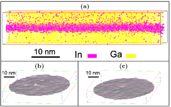
APT experiments were conducted in pulsed laser mode with a pulse energy of 0.012 nJ using a Cameca LEAP 3000X HR, where the base temperature of the sample was set at 30 K and a constant detection rate of 0.01 atoms per pulse was employed. The IVAS software package (CAMECA Version 3.6.6) was used to carry out APT reconstruction and analysis was informed by the thicknesses of the (In,Ga)N and GaN layers measured by XRD and transmission electron microscopy (TEM) and also the geometry of the tip as measured by scanning electron microscopy (SEM). The In content of the sample was analyzed using concentration profiles through each QW computed using a proximity histogram (proxigram) approach as described in Ref. Tang et al., 2015a. The mean In fractions across the five QWs based on the maxima of the In concentration profiles is 17.00.6%, which is in good agreement with the XRD data. While frequency distribution analysis of -plane QWs provides no evidence for the formation of nonrandom indium clusters, Galtrey et al. (2007) recent studies of nonpolar -plane QWs with a similar In content (15%) to the -plane samples studied here have presented clear evidence for the presence of clustering. Tang et al. (2015a) For the sample under discussion here, the question of clustering is less clear-cut. Evidence of clustering is sensitively dependent on the exact parameters of the analysis used, and the issue is still under investigation. However, in this paper we model the QW as a random alloy and assess the extent to which this model can accurately reproduce the observed optical properties, which can provide an insight into the relative importance of slight deviations from randomness in these QWs, if present. More details of the APT analysis will be reported in Ref. Tang et al., 2015b.
An isoconcentration surface analysis of the APT data similar to that performed by Galtrey et al. Galtrey et al. (2007) has been performed to assess whether the roughness of the upper interface of the QWs [at which GaN is grown on (In,Ga)N] is rougher than the lower interface of the QWs [at which (In,Ga)N is grown on GaN] and typical data are shown in Fig. 1 for an indium concentration at the isosurface of 5%. This yields a roughness for the lower surface of 0.24 nm (root mean square), but a larger roughness for the upper surface of 0.48 nm, with the increased roughness largely relating to raised island-like features a few nm in diameter and 1-2 monolayers in height, consistent with the monolayer and bilayer well-width fluctuations previously observed on the plane. High-resolution scanning transmission electron microscopy imaging of the surfaces of the QWs also indicates the existence of surface roughness. Although the projection problem makes it difficult to distinguish the exact nature of the roughness observed in STEM, the data are consistent with the APT observations.
III.2 Structural characterization: Input into the theoretical framework
Based on the experimental data discussed in Sec. III.1, we take the -plane QW width to be approximately 2 nm. We include in our calculations disklike 2 monolayer thick well-width fluctuations at one of the QW interfaces. This is a reasonable representation of the well-width fluctuations that have been observed in APT and is consistent with earlier approaches to the modeling of such features. Watson-Parris et al. (2011) However, for the -plane QW structure considered here, we do not expect that 2 monolayer thick well-width fluctuations are of central importance for the description of the electronic and optical properties. This assumption is based on the fact that in an -plane QW the macroscopic field is absent. Therefore, in contrast to a -plane system, the wave functions in an -plane system are not localized near the interface between QW and barrier material, since there is no field causing this form of localization. Consequently, the wave functions are expected to be far less sensitive to the shape and diameter of the well-width fluctuations. As we will show below, this assumption is consistent with the result of our calculations. The In content in the sample has been measured to be 18.30.7% (XRD) and 17.00.6% (APT), respectively. For our calculations we have set the QW In content to 17%, close to the measured values. We use here SCs with a size of nm3, thus containing approximately 82,000 atoms, with periodic boundary conditions. Based on the APT data discussed in Sec. III.1, we treat (In,Ga)N as a random alloy. To be able to perform a detailed comparison with experiment and to allow for reasonable statistical averages, our calculations have been repeated 75 times for the fixed In fraction of 17%. This allows us to realize a large number of microscopically different random configurations in a large SC, where we have nominally the same In content in the SC but the positions of the In atoms have been changed randomly.
IV Electronic and optical properties: Experiment and theory
Having investigated the structural properties of the sample, we turn now to study the electronic and optical properties of the -plane (In,Ga)N/GaN QW system. We start in Sec. IV.1 by describing the experimental methods used for the optical characterization, followed by the discussion of the experimental results in Sec. IV.2. We then briefly introduce the theoretical framework in Sec. IV.3, while Sec. IV.4 focuses on the comparison of theoretical and experimental data.
IV.1 Experimental setup
The PL and P-PLE studies were carried out either using excitation from a cw He/Cd laser or using a combination of a 300 W xenon lamp and monochromator as a fixed or tunable wavelength excitation source. The sample was mounted in the cryostat so that the axis of the GaN was horizontal. The PL from the sample was analyzed by a 0.85 m double-grating spectrometer and a Peltier-cooled GaAs photomultiplier using standard lock-in detection techniques. The spectral dependence of the DOLP of the emission was determined by measuring the PL spectra polarized in the plane parallel () and perpendicular () to the axis of the sample. Once the spectra are obtained, the DOLP is calculated from Sun et al. (2003)
| (1) |
where () is the PL intensity for the electric field perpendicular (parallel ) to the axis.
A time-correlated single-photon counting system was used for the time decay measurements. For these studies the exciting light was generated by a mode-locked Ti:sapphire laser with a frequency-tripled emission output of 4.88 eV. A spectrometer followed by a micro channel plate detector was used to detect the emitted light.
IV.2 Experimental results: Optical characterization
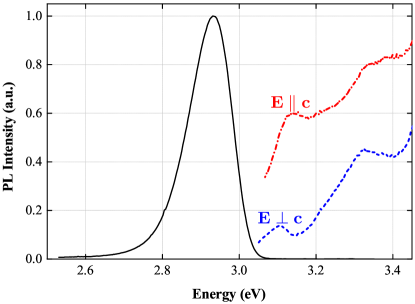
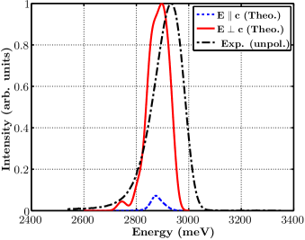
In this section we describe the results of our PL, P-PLE, and time decay measurements at 10 K on the -plane (In,Ga)N/GaN QW sample described above. Figure 2 shows the P-PLE spectra with the plane of polarization of the incident light either perpendicular () or parallel () to the axis of the crystal. Figure 2 also displays the (unpolarized) PL spectrum of the sample (solid black line). We note several specific aspects of the PL spectrum. First, the full width at half maximum (FWHM) of the PL spectrum is 135 meV. This value is much larger than typical FWHM values found in -plane systems. Watson-Parris (2011) Although it should be noted that the PL spectrum exhibits an extended low-energy tail, we have shown previously Sutherland et al. (2015) that in our samples this low-energy tail arises from recombination in QWs present on semipolar facets which form at step bunches associated with the miscut of the GaN substrate. These semipolar QWs have higher QW width and In content than the nonpolar QWs on the adjoining -plane terraces on either side of the step, and thus emit at longer wavelength. We do not aim to include such structures in our model or reproduce this aspect of the spectra here. The emission from the semi-polar QWs is of secondary importance in determining the magnitude of the spectral width. Second, the energy difference (Stokes shift) between the peak of the lowest exciton transition in the P-PLE spectrum and the peak of the PL spectra is 180 meV. We also note an energy splitting between the two lowest exciton transitions for the two polarizations of the excitation light of 35 meV. We attribute this splitting mainly to the crystal field splitting energy in the (In,Ga)N system. Yan et al. (2011)
The values of the linewidth and Stokes shift, based on the assumption that the emission is an intrinsic process, are strongly suggestive of emission involving strongly localized carriers. As to the nature of the localization we anticipate that, similarly to -plane systems, alloy fluctuations will play a major role.
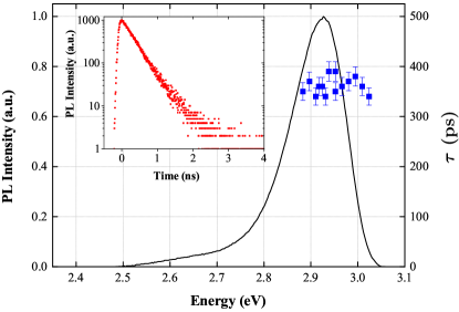
To help further understand the nature of the recombination we performed PL time decay measurements across the spectrum. The results of these measurements are depicted in Fig. 3. Interestingly, our measurements reveal that the PL decays are single exponentials with characteristic time constants ps over the majority of the spectrum. Throughout this work we assume that the recombination is purely radiative and the values of are the radiative decay constants. This assumption is supported by temperature-dependent measurements (not shown) and the fact that the values of found here are similar to those of Marcinkevicius et al. Marcinkevicius et al. (2013), also measured at low temperature. The data reported by Marcinkevicius et al. Marcinkevicius et al. (2013) at low temperature were shown to be not influenced by nonradiative recombination. Only on the low-energy side of the spectra did we find more slowly decaying emission as we have reported elsewhere. Sutherland et al. (2015) The emission on the low-energy side is attributed to semipolar QWs at step bunches described above. The decay time from the emission associated with these semi-polar QWs occurs on a longer time scale due to the locally present built-in field, which separates the electron/hole wave functions.
It is important to note that the radiative decay dynamics observed here are in stark contrast to -plane (In,Ga)N QW structures. Pozina et al. (2000); Morel et al. (2003); Graham et al. (2005); Davies et al. (2014) First, in polar (In,Ga)N QWs the decay occurs over a much longer time scale due to the polarization field perpendicular to the plane of the QWs. Pozina et al. (2000); Graham et al. (2005); Brosseau et al. (2010); Davies et al. (2014) Second, the decay curves are nonexponential due to the variable in-plane separation of the separately localized electrons and holes. Morel et al. (2003); Brosseau et al. (2010) Single-exponential decays in nonpolar QWs have also been reported by other groups. Garrett et al. (2009); Marcinkevicius et al. (2013) The explanation proposed for the nature of the decay transients is that recombination involves localized excitons. Garrett et al. (2009); Marcinkevicius et al. (2013)
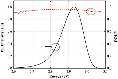
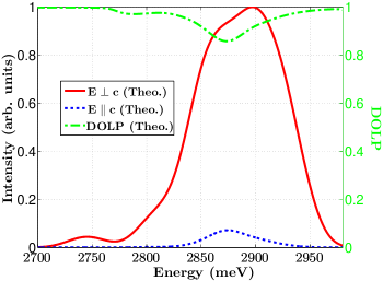
As discussed in the introduction, nonpolar QWs should exhibit a high DOLP. This should be particularly the case at 10 K, bearing in mind the splitting of the lowest valence band states as revealed by the PLE measurements shown in Fig. 2. The measured DOLP of the -plane (In,Ga)N/GaN QW sample at 10 K, based on the method described in Sec. IV.1, is shown in Fig. 4 together with the (unpolarized) PL spectrum. We find a very high DOLP (%), which is in good agreement with other experimental data on -plane (In,Ga)N/GaN QWs. Sun et al. (2003); Kubota et al. (2008); Matioli et al. (2012) Theoretically, based on continuum-like descriptions, at the VBE one would expect a very high DOLP for several reasons. First, assuming growth along the direction, the QW confinement lifts the degeneracy of the - and -like valence band states due to their different effective masses along the growth direction. Sun et al. (2003); Schulz et al. (2010); Matioli et al. (2012) Second, - and -like states are energetically separated by the crystal field splitting energy in (In,Ga)N alloys. Yan et al. (2011) Thus, the VBE is expected to be predominately -like. Figure 4 shows that the DOLP is almost constant over the entire spectrum. Only on the low-energy side of the spectrum do we find a small reduction in the DOLP. This reduction is to be expected as the low-energy part of the PL spectrum originates from recombination involving semipolar QW states. The detailed strain state of such QWs on nanoscale facets associated with step bunches is not straightforward to predict and might cause increased band mixing effects and consequently a reduced DOLP. A detailed investigation of these semipolar contributions is beyond the scope of the present study. Overall, given that the PL linewidth exceeds the valence band splitting, it is not immediately obvious why the DOLP, shown in Fig. 4, is virtually constant across the spectrum. One possible answer is that the PL emission spectrum originates almost entirely from transitions involving localized states in different potential fluctuations. Therefore, calculations including random alloy fluctuations are required to shed more light on this behavior. In the next section we introduce the theoretical framework used to address these questions.
IV.3 Theoretical Framework
We use an atomistic TB model to study the electronic and optical properties of -plane (In,Ga)N-based QWs. This approach allows us to include (random) alloy fluctuations in the QW region and the resulting local strain and built-in potential fluctuations on a microscopic level. The strain field calculations are based on a modified valence force field model accounting for electrostatic corrections in addition to bond bending, bond stretching and related cross-terms. Schulz et al. (2015b) Local built-in field fluctuations are treated on the basis of our recently developed local polarization theory. Caro et al. (2013) Strain and built-in field fluctuations are included in the TB model presented in Ref. Caro et al., 2013. The bulk TB parameters were determined from fitting TB band structures to hybrid functional (HSE) DFT band structures, showing a very good agreement between the TB and HSE-DFT band structures. The TB parameters and the TB model are discussed in detail in Ref. Caro et al., 2013. The application of the TB model to QW structures, including the coupling of the TB model to CI calculations to include excitonic effects, is discussed in detail in Ref. Schulz et al., 2015b. The model has already been benchmarked against experimental and DFT data on bulk (In,Ga)N alloys, revealing a very good agreement between experiment, DFT, and TB results. Caro et al. (2013) Moreover, our recent calculations on electronic and optical properties of -plane (In,Ga)N/GaN QWs show also a very good agreement with available experimental data. Schulz et al. (2015b) The model can directly be applied, without modification of the theoretical framework, to -plane structures. Here, only the orientation of the QW structure in the simulation SC has to be changed compared to a -plane system. The numerical and structural details of the system considered here (QW width, In content, number of atoms in the SC, SC size, etc.) have already been discussed in Sec. III.2.
IV.4 Theoretical results: Electronic structure and optical properties
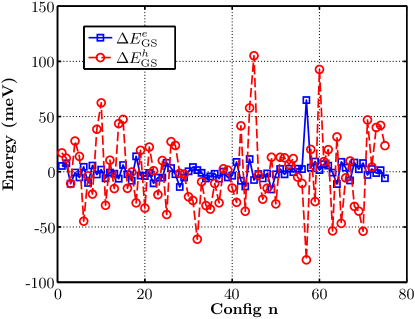
Equipped with the knowledge about the experimental data, we present here the results of the TB calculations. Figure 5 shows the variation of the single-particle electron and hole ground state energies with respect to the average ground state energy for electrons and holes , respectively, as a function of the configuration (Config) number . From Fig. 5 we can infer that variations in the electron ground state energies are much smaller than the variations in the hole ground state energies . This is also reflected in the calculated standard deviations . For electrons we find a standard deviation of meV, while the standard deviation for the hole ground state energy is meV. We have observed a similar behavior in -plane (In,Ga)N/GaN QWs. Schulz et al. (2015b)
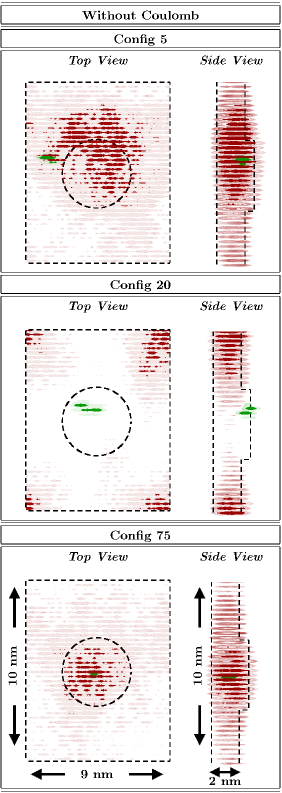
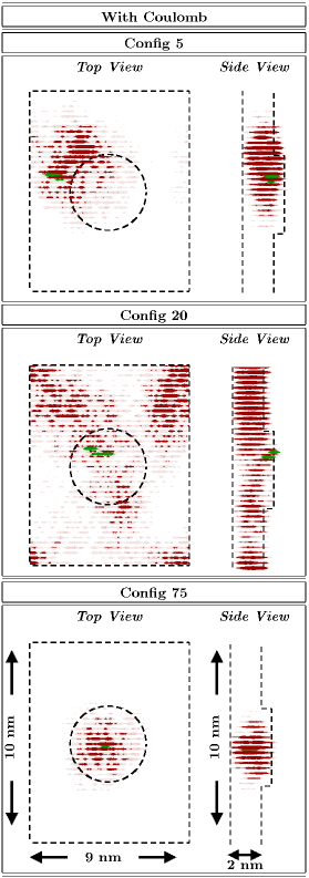
The strong variations in the hole ground state energies in -plane systems are attributed to hole wave function localization effects due to random alloy fluctuations. Watson-Parris et al. (2011); Yang et al. (2014); Schulz et al. (2015b) To confirm this behavior in a nonpolar system, Fig. 6 shows isosurfaces of the single-particle electron (red) and hole (green) ground state charge densities for configurations 5, 20, and 75, which reflect typical situations observed in the random alloy as we will discuss below. The light and dark isosurfaces correspond to 5% and 25% of the maximum charge density values, respectively. From Fig. 6 one can infer that the random alloy fluctuations lead to strong hole wave function localization effects, independently of the configuration. In general we find that the alloy fluctuations have a much weaker effect on the electron wave functions, when compared with the holes. As expected from our discussion in Sec. III.2, 2 monolayer thick well-width fluctuations do not contribute significantly to wave function localization effects. Unless very deep well-width fluctuations are present, which would generate large -oriented surface areas, we do not expect that well-width fluctuations change the localization characteristics of electron and hole wave functions in comparison to the here presented data. Therefore, we conclude that in -plane QW structures, grown on freestanding GaN substrates, localization effects can be mainly attributed to alloy fluctuations. Looking at the displayed configurations in more detail, for configuration 5, the electron wave function is almost spread out over the entire QW area, with perturbations introduced by the alloy fluctuations. We observe slightly stronger perturbations in the case of configurations 20 and 75 (cf. Fig. 6). Overall there is a clear difference in the wave function localization characteristics between electrons and holes. All this shows that a continuum-based description might give, to a first approximation, a reasonable description of the ground state electron wave functions but would fail for the description of the hole ground states. One should also note that the differences in the localization features of the different electron single-particle states, as discussed above, are important. For instance, in configuration 75 the electron charge density is mainly localized in the region where the hole ground state is localized. Consequently, one could expect a higher wave function overlap between electron and hole. For configuration 5, the electron ground state charge density has stronger contributions (dark red isosurfaces) in areas spatially separated from the strongly localized hole ground state. This is even more pronounced for configuration 20 (cf. Fig. 6).
In general, the observed asymmetry in the localization characteristics of electron and hole ground state wave functions is consistent with DFT-based calculations for bulk (In,Ga)N alloys, Liu et al. (2010); Schulz et al. (2015a) and explains the observed asymmetry in the electron and hole ground state energy variations displayed in Fig. 5. While the local atomic arrangement (In-N-In chains) is of secondary importance for the electrons, it is of central importance for the hole ground states, as shown by DFT-based calculations. Liu et al. (2010); Schulz et al. (2015a) Thus, different microscopic arrangements of In atoms will give very different hole ground state energies. This picture of localized hole and delocalized electrons is not quite compatible with the experimentally observed decay times being constant across the spectrum, as we would still expect some variation in the electron and hole in-plane wave function overlap leading to a range of radiative recombination times, i.e., nonexponential decay curves. It should however be noted that the effect would be much less marked than in the case of polar QWs where the electrons and holes are localized separately. We will discuss this discrepancy later.
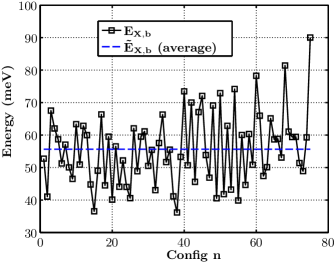
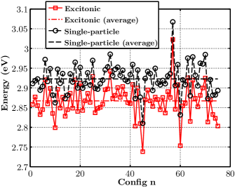
The variations in the single-particle energies will also affect the single-particle ground state emission energies. This is shown in Fig. 7. The single-particle transition energies (black circles) show large variations between 2.81 eV and 3.07 eV. The average single-particle transition energy is around 2.93 eV (black dashed line). However, to be able to compare the theoretical ground state emission energies with the experimental PL emission energies, we have to include Coulomb (excitonic) effects. We use the CI scheme described in detail in our previous work, to include excitonic effects in the description. Schulz et al. (2015b) We assume here a single electron-hole pair. Thus, electron-electron and hole-hole Coulomb interactions are not considered. We neglect electron-hole exchange contributions since these are small corrections on the energy scale relevant for the discussion of our results. To describe the excitonic many-body wave function we include 5 electron and 15 hole states in the CI expansion. The calculated excitonic ground state energies (red squares) are shown in Fig. 7 again as a function of the configuration number . The average excitonic transition energy is given by the (red) dashed dotted line. From Fig. 7 we conclude that Coulomb effects introduce a significant shift and broadening of the spectrum when compared with the single-particle results. However, when calculating the excitonic binding energy as the difference between the single-particle ground state transition energy and the excitonic ground state transition energy, we find also large variations in . The excitonic binding energy is displayed in Fig. 8 as a function of the configuration number . The calculated values scatter between 36 meV and 90 meV. On average we find here an excitonic binding energy of approximately 56 meV (dashed line). The difference in the observed excitonic binding energies can be understood from the single-particle wave functions shown in Fig. 6. We find that for configuration 20 the electron wave function, in comparison to configurations 5 and 75, shows very little charge density in the spatial region where the hole is localized, leading in the single-particle picture to a reduced wave function overlap. From this one could expect a lower exciton binding energy in comparison to a configuration where electron and hole wave functions are localized in the same spatial region. As shown in Fig. 6, this is the situation for configuration 75, which has consequently a very large excitonic binding energy (cf. Fig. 8). The intermediate situation is realized for configuration 5 giving also an intermediate excitonic binding energy. In general it is important to note that excitonic binding energies in nonpolar QWs are much larger than in -plane systems. This effect is expected due to the absence of the macroscopic built-in field in nonpolar nitride-based QWs. Wei et al. (2012); Funato and Kawakami (2008)
To shed even more light onto the impact of the Coulomb interaction on the wave functions, we use reduced electron and hole density matrices to visualize the electron and hole densities under the influence of the Coulomb interaction. In general, the excitonic many-body wave function can be written as a linear combination of electron-hole basis states:
| (2) |
Here is the vacuum state, the expansion coefficient, and () denotes the electron (hole) creation operator. Electron and hole states are denoted by and , respectively. We can then define reduced density matrices for electrons and holes. For instance, for the electrons the density operator is given by:
| (3) |
The corresponding electron and hole densities are given by and , respectively. Figure 9 depicts the calculated electron and hole densities for the configurations 5, 20, and 75. We can infer from Fig. 9 that while the hole charge density is almost unchanged in comparison to the single-particle description (cf. Fig. 6), the electron charge density is significantly affected by the attractive Coulomb interaction between electron and hole. The electron charge density, under the influence of the Coulomb interaction, localizes about the hole for all configurations. Thus our atomistic model predicts exciton localization in nonpolar (In,Ga)N/GaN QWs. This behavior is consistent with the experimental observation of single-exponential PL decay transients discussed in detail in Sec. IV.2 and observed experimentally by other groups. Garrett et al. (2009); Marcinkevicius et al. (2013) Also the strong wave function overlap independent of the hole localization is consistent with the measured decay times being constant over the spectrum.
To further compare the theoretical results with the experimental PL data, we have calculated the excitonic ground state emission spectrum following Ref. Schulz et al., 2015b. Since the experiment indicates a large DOLP () we have performed calculations for two different light polarization vectors , namely and . This means that the selected electric field is perpendicular to the axis () and parallel to the axis (), respectively. In the calculations we have assumed growth along the axis; therefore the chosen light polarization vectors reflect the experimental setup described in Sec. IV.1. The calculated excitonic ground state emission spectrum is shown in Fig. 10 for (red solid line) and (blue dashed line) together with the experimental (unpolarized) PL emission spectrum (black dashed-dotted line). Several different features are visible in Fig. 10.
First of all we find a good agreement between the calculated (solid red) and the experimentally determined emission energy (black dashed-dotted line), given the slight uncertainties in In content and well width as discussed in Sec. III.1. Second, we find also theoretically a very broad emission spectrum. For (), the theoretically determined FWHM is approximately 101 meV. Experimentally we find a FWHM value of 135 meV. Different factors might contribute to the observed differences between theory and experiment. For example, even though 75 different microscopic structures may appear a large number, it could be the case that even more configurations have to be considered to fully resolve the measured FWHM, bearing in mind the large variations between different microscopic configurations (cf. Fig. 5). Additionally, if subtle nonrandom clustering effects exist, they may contribute to the broadening of the PL linewidth. However, the theoretically determined value of 101 meV for the FWHM is in reasonable agreement with the experimental data. Third, Fig. 10 shows that there is a large difference in the calculated intensities for and . In the theoretical analysis, the intensities are normalized to the intensity of . If we calculate the DOLP from our theoretical spectrum via Eq. (1) based on the maximum intensities for and , we find a value of approximately 87%, which is slightly smaller than the experimental values (%).
To compare our theoretical results in more detail with the experiment, we have also calculated the spectral dependence of the DOLP from our theoretical emission spectra for the two light polarization configurations depicted in Fig. 10. Using Eq. (1), our theoretical results for the spectral dependence of the DOLP are shown in Fig. 11. Similarly to Fig. 4, the DOLP (green dashed-dotted line) is shown together with the excitonic emission spectrum for (red solid line) and (blue dashed line). When comparing our theoretical data with the experimental data shown in Fig. 4, the theoretical results show slightly lower values than the experiment, plus the calculated DOLP is not as constant as the experimental data across the spectrum. Again, even though 75 configurations may appear a large number, we show below that some of the structure in the DOLP spectrum of Fig. 11 is due to a small number of exceptional states; more configurations would be required to reliably treat the importance of such states. This is beyond the scope of the present study, since the present analysis gives already, in general, a good description of the experimentally observed spectral dependence of the DOLP.
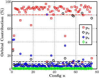
All in all the theoretical calculations indicate that random alloy fluctuations, explicitly taken into account in our model, affect the DOLP only slightly. The origin of the calculated high DOLP can be further understood by looking at the orbital character of the hole ground state/VBE state. The outcome of such an analysis is displayed in Fig. 12, where the orbital contributions to the VBE are shown as a function of the configuration number . From a continuum-based calculation, neglecting the weak spin-orbit coupling, one would expect, due to the differences in the valence band effective masses along the growth direction and the positive crystal field splitting energy in GaN and InN, that the VBE is dominated by a single-orbital type (- or -like orbitals). Obviously such an analysis neglects the effects of alloy fluctuations. However, we can infer from Fig. 12 that the VBE state in the different microscopic configurations is mainly made up of contributions from a single orbital type, in this case from -like orbitals. Thus, for the orbital character of the hole ground state the microscopic configuration is, in general, of secondary importance, although we note that there is an enhanced -like character and a very low -like character in about 10%-20% of the structures studied. The dominance of the character of the VBE explains the calculated high DOLP, which is in good agreement with the experimental data. Furthermore, as we know from Fig. 5 the hole ground state energies vary significantly between different configurations. This gives rise to the broad emission spectrum shown in Fig. 10. Since Fig. 12 reveals that the orbital contribution to the VBE state is for the most part independent of the configuration number , all these findings in combination explain why we observe only a weak spectral dependence of the DOLP displayed in Fig. 11, in line with the experimental results displayed in Fig. 4.
V Conclusion
In summary, we have presented a detailed experimental and theoretical analysis of the structural, electronic, and optical properties of -plane (In,Ga)N/GaN QWs. The structural characterization using XRD, STEM, and APT provide us with consistent parameters for the QW composition and dimensions and suggest that we may reasonably model the (In,Ga)N as a random alloy, although we are not able to rule out the possibility of some subtle deviations of the In distribution from randomness. In addition to the structural characterization, we used PL, P-PLE, and time-resolved PL measurements to analyze the optical properties of the system under consideration. Our results show a high DOLP, single-exponential PL decay transients, strong Stokes shifts, and a very broad PL linewidth. The strong Stokes shift and the broad PL line width are indicative of strong carrier localization effects, while single-exponential PL decay transients in nonpolar (In,Ga)N QWs are usually attributed to exciton localization effects. To shed further light on the experimentally observed properties, we have employed an atomistic TB model to achieve a microscopic description of the electronic structure of the -plane system including, on an atomistic level, strain and built-in field variations arising from the considered random alloy fluctuations. To be able to compare with the measured optical spectra, our model includes also excitonic effects via the CI scheme. The results of our calculations reveal strong hole wave function localization effects originating from random alloy fluctuations. We find that alloy fluctuations have a much weaker effect on the electron wave functions. The observed localization effects lead to a significant broadening of the single-particle ground state energies and therefore the corresponding transition energies. When including Coulomb effects in the calculations we observe compared to -plane systems strongly increased excitonic binding energies. This can be attributed to the absence of the macroscopic built-in field in the nonpolar -plane system studied here. Coulomb effects lead also to the situation where the electron wave function localizes about the hole. In other words, the theoretical calculations predict exciton localization effects, which are consistent with the single-exponential decay of the PL transients observed in the experiment. Moreover, when calculating the excitonic ground state emission spectrum we find a good agreement with the experimental PL spectra both in terms of FWHM and PL peak position energy. Additionally, when calculating the DOLP, the theoretical data are in good agreement with the experimental result of a very high DOLP. Our findings indicate that the DOLP is, in general, only slightly affected by random alloy fluctuations. However, since the observed PL line width is larger than the measured valence band splitting, wave function localization effects due to random alloy fluctuations are required to explain the spectral independence of the DOLP, given that the theoretical analysis shows that these localized states are dominated by a single orbital type. Overall, this combined experimental and theoretical analysis provides clear insight into the basic physical properties of -plane (In,Ga)N/GaN QWs.
Acknowledgements.
This work was supported by Science Foundation Ireland (Projects No. 13/SIRG/2210 and 10/IN.1/I2994), the United Kingdom Engineering and Physical Sciences Research Council (Grant Agreements No. EP\J001627\1 and EP\J003603\1), the European Union 7th Framework Programme DEEPEN (Grant Agreement No. 604416), and in part by the European Research Council under the European Community’s 7th Framework Programme (FP7/2007-2013)/ERC Grant Agreement No. 279361 (MACONS). We would like to acknowledge the help of D. Haley, University of Oxford, on the APT results. S. S. acknowledges computing resources provided by Science Foundation Ireland (SFI) to the Tyndall National Institute and by the SFI and Higher Education Authority Funded Irish Centre for High End Computing. Supporting data may be accessed via the following link: https://www.repository.cam.ac.uk/handle/1810/252770.References
- Nakamura et al. (1993) S. Nakamura, M. Senoh, and T. Mukai, J. Appl. Phys. 32, L8 (1993).
- Nakamura et al. (1994) S. Nakamura, T. Mukai, and M. Senoh, Appl. Phys. Lett. 64, 1687 (1994).
- Bernardini et al. (1997) F. Bernardini, V. Fiorentini, and D. Vanderbilt, Phys. Rev. B 56, R10024 (1997).
- Im et al. (1998) J. S. Im, H. Kollmer, J. Off, A. Sohmer, F. Scholz, and A. Hangleiter, Phys. Rev. B 57, R9435 (1998).
- Leroux et al. (1998) M. Leroux, N. Grandjean, M. Laügt, J. Massies, B. Gil, P. Lefebvre, and P. Bigenwald, Phys. Rev. B 58, R13371 (1998).
- Fiorentini et al. (1999) V. Fiorentini, F. Bernardini, F. Della Sala, A. Di Carlo, and P. Lugli, Phys. Rev. B 60, 8849 (1999).
- Waltereit et al. (2000) P. Waltereit, O. Brandt, A. Trampert, H. T. Grahn, J. Menniger, M. Ramsteiner, and K. H. Ploog, Nature 406, 865 (2000).
- Kim et al. (2007) K. C. Kim, M. C. Schmidt, H. Sato, F. Wu, N. Fellows, M. Saito, K. Fujito, J. S. Speck, S. Nakamura, and S. P. DenBaars, Phys. Status Solidi RRL 1, 125 (2007).
- Schwarz and Kneissl (2007) U. T. Schwarz and M. Kneissl, Phys. Status Solidi RRL 1, A44 (2007).
- Kappers et al. (2007) M. J. Kappers, J. L. Hollander, C. McAleese, C. F. Johnston, R. F. Broom, J. S. Barnard, M. E. Vickers, and C. J. Humphreys, J. Cryst. Growth 300, 155 (2007).
- Gühne et al. (2008) T. Gühne, Z. Bougrioua, S. Laugt, M. Nemoz, P. Vennegues, B. Vinter, and M. Leroux, Phys. Rev. B 77, 075308 (2008).
- Paskova (2008) T. Paskova, phys. stat. sol. (b) 245, 1011 (2008).
- Badcock et al. (2009) T. J. Badcock, P. Dawson, M. J. Kappers, C. McAleese, J. L. Hollander, C. F. Johnston, D. V. S. Rao, A. M. Sanchez, and C. J. Humphreys, J. Appl. Phys. 105, 123112 (2009).
- Schulz et al. (2010) S. Schulz, T. J. Badcock, M. A. Moram, P. Dawson, M. J. Kappers, C. J. Humphreys, and E. P. O’Reilly, Phys. Rev. B 82, 125318 (2010).
- Zhao et al. (2011) Y. Zhao, S. Tanaka, C.-C. Pan, K. Fujito, D. Feezell, J. S. Speck, S. P. DenBaars, and S. Nakamura, Appl. Phys. Express 4, 082104 (2011).
- Seo et al. (2011) Y. G. Seo, K. H. Baik, H. Song, J.-S. Son, K. Oh, and S.-M. Hwang, Optics Express 19, 12919 (2011).
- Pan et al. (2012) C. C. Pan, S. Tanaka, F. Wu, Y. Zhao, J. S. Speck, S. Nakamura, S. P. DenBaars, and D. Feezell, Appl. Phys. Express 5, 062103 (2012).
- Scholz (2012) F. Scholz, Semicond. Sci. Technol. 27, 024002 (2012).
- Matioli et al. (2012) E. Matioli, S. Brinkley, K. Kelchner, Y.-L. Hu, S. Nakamura, S. DenBaars, J. Speck, and C. Weisbuch, Light: Science & Applications 1, e22 (2012).
- Kundys et al. (2014) D. Kundys, S. Schulz, F. Oehler, D. Sutherland, T. J. Badcock, P. Dawson, M. J. Kappers, R. A. Oliver, and C. J. Humphreys, J. Appl. Phys. 115, 113106 (2014).
- Sutherland et al. (2015) D. Sutherland, T. Zhu, J. T. Griffiths, F. Tang, P. Dawson, D. Kundys, F. Oehler, M. J. Kappers, C. J. Humphreys, and R. A. Oliver, Phys. Stat. Sol b 252, 965 (2015).
- Sun et al. (2003) Y.-J. Sun, O. Brandt, M. Ramsteiner, H. T. Grahn, and K. H. Ploog, Appl. Phys. Lett. 82, 3850 (2003).
- Wang et al. (2012) H. Wang, Z. Ji, S. Qu, G. Wang, Y. Jiang, B. Liu, X. Xu, and H. Mino, Optics Express 20, 3932 (2012).
- Hammersley et al. (2012) S. Hammersley, D. Watson-Parris, P. Dawson, M. J. Godfrey, T. J. Badcock, M. J. Kappers, C. McAleese, R. A. Oliver, and C. J. Humphreys, J. Appl. Phys. 111, 083512 (2012).
- Galtrey et al. (2007) M. J. Galtrey, R. A. Oliver, M. J. Kappers, C. J. Humphreys, D. J. Stokes, P. H. Clifton, and A. Cerezo, Appl. Phys. Lett. 90, 061903 (2007).
- Tang et al. (2015a) F. Tang, T. Zhu, F. Oehler, W. Y. Fu, J. T. Griffiths, F. C.-P. Massabuau, M. J. Kappers, T. L. Martin, P. A. J. Bagot, M. P. Moody, et al., Appl. Phys. Lett. 106, 072104 (2015a).
- Funato and Kawakami (2008) M. Funato and Y. Kawakami, J. Appl. Phys. 103, 093501 (2008).
- Watson-Parris et al. (2011) D. Watson-Parris, M. J. Godfrey, P. Dawson, R. A. Oliver, M. J. Galtrey, M. J. Kappers, and C. J. Humphreys, Phys. Rev. B 83, 115321 (2011).
- Yang et al. (2014) T.-J. Yang, R. Shivaraman, J. S. Speck, and Y.-R. Wu, J. Appl. Phys. 116, 113104 (2014).
- Liu et al. (2010) Q. Liu, J. Lu, Z. Gao, L. Lai, R. Qin, H. Li, J. Zhou, and G. Li, Phys. Stat. Sol B 247, 109 (2010).
- Schulz et al. (2015a) S. Schulz, O. Marquardt, C. Coughlan, M. A. Caro, O. Brandt, and E. P. O’Reilly, in Proc. SPIE 9357, Physics and Simulation of Optoelectronic Devices XXIII, edited by B. Witzigmann, M. Osinski, F. Henneberger, and Y. Arakawa (SPIE, San Francisco, CA, 2015a), p. 93570C.
- Bester (2009) G. Bester, J. Phys.: Condens. Matter 21, 023202 (2009).
- Camacho Mojica and Niquet (2010) D. Camacho Mojica and Y.-M. Niquet, Phys. Rev. B 81, 195313 (2010).
- der Maur (2015) M. A. der Maur, J. Comput. Electron. 14, 398 (2015).
- Schulz et al. (2015b) S. Schulz, M. A. Caro, C. Coughlan, and E. P. O’Reilly, Phys. Rev. B 91, 035439 (2015b).
- Molina-Sánchez et al. (2012) A. Molina-Sánchez, A. García-Cristóbal, and G. Bester, Phys. Rev. B 86, 205430 (2012).
- Franceschetti et al. (1999) A. Franceschetti, H. Fu, L. W. Wang, and A. Zunger, Phys. Rev. B 60, 1819 (1999).
- Schulz et al. (2006) S. Schulz, S. Schumacher, and G. Czycholl, Phys. Rev. B 73, 245327 (2006).
- Kucharski et al. (2012) R. Kucharski, M. Zajac, R. Doradzinski, M. Rudzinski, R. Kudrawiec, and R. Dwilinski, Semicond. Sci. Technol. 27, 024007 (2012).
- Pendlebury et al. (2007) S. T. Pendlebury, P. J. Parbrook, D. J. Mowbray, D. A. Wood, and K. B. Lee, J. Cryst. Growth 307, 363 (2007).
- Tang et al. (2015b) F. Tang, T. Zhu, F. Oehler, W. Y. Fu, J. S. Barnard, S. Zhang, J. T. Griffiths, M. J. Kappers, R. A. Oliver, T. Martin, et al., In prepartion (2015b).
- Watson-Parris (2011) D. T. S. Watson-Parris, Carrier Localization in InGaN/GaN Quantum Wells, PhD Thesis University of Manchester, (2011), https://www.escholar.manchester.ac.uk/uk-ac-man-scw:132844.
- Yan et al. (2011) Q. Yan, P. Rinke, M. Winkelnkemper, A. Qteish, D. Bimberg, M. Scheffler, and C. G. Van de Walle, Semicond. Sci. Technol. 26, 014037 (2011).
- Marcinkevicius et al. (2013) S. Marcinkevicius, K. M. Kelchner, L. Y. Kuritzky, S. Nakamura, S. P. DenBaars, and J. S. Speck, Appl. Phys. Lett. 103, 111107 (2013).
- Pozina et al. (2000) G. Pozina, J. P. Bergman, B. Monemar, T. Takeuchi, H. Amano, and I. Akasaki, J. Appl. Phys. 88, 2677 (2000).
- Morel et al. (2003) A. Morel, P. Lefebvre, S. Kalliakos, T. Taliercio, T. Bretagnon, and B. Gil, Phys. Rev. B 68, 045331 (2003).
- Graham et al. (2005) D. M. Graham, A. Soltani-Vala, P. Dawson, M. J. Godfrey, T. M. Smeeton, J. S. Barnard, M. J. Kappers, C. J. Humphreys, and E. J. Thrush, J. Appl. Phys. 97, 103508 (2005).
- Davies et al. (2014) M. J. Davies, P. Dawson, F. C.-P. Massabuau, R. A. Oliver, M. J. Kappers, and C. J. Humphreys, Appl. Phys. Lett. 105, 092106 (2014).
- Brosseau et al. (2010) C.-N. Brosseau, M. Perrin, C. Silva, and R. Leonelli, Phys. Rev. B 82, 085305 (2010).
- Garrett et al. (2009) G. A. Garrett, H. Shen, M. Wraback, A. Tyagi, M. C. Schmidt, J. S. Speck, S. P. DenBaars, and S. Nakamaura, Phys. Stat. Solidi (c) 6, S800 (2009).
- Kubota et al. (2008) M. Kubota, K. Okamoto, T. Tanaka, and H. Ohta, Appl. Phys. Lett. 92, 011920 (2008).
- Caro et al. (2013) M. A. Caro, S. Schulz, and E. P. O’Reilly, Phys. Rev. B 88, 214103 (2013).
- Wei et al. (2012) S. Wei, Y. Jia, and C. Xia, Superlattices Microstruct. 51, 9 (2012).