üü \newunicodecharöö \newunicodecharÖÖ \newunicodecharøø \newunicodecharáá \newunicodecharΓΓ
Synthesis of Epitaxial Single-Layer MoS2 on Au(111)
Abstract
We present a method for synthesizing large area epitaxial single-layer MoS2 on the Au(111) surface in ultrahigh vacuum. Using scanning tunneling microscopy and low energy electron diffraction, the evolution of the growth is followed from nanoscale single-layer MoS2 islands to a continuous MoS2 layer. An exceptionally good control over the MoS2 coverage is maintained using an approach based on cycles of Mo evaporation and sulfurization to first nucleate the MoS2 nano-islands and then gradually increase their size. During this growth process the native herringbone reconstruction of Au(111) is lifted as shown by low energy electron diffraction measurements. Within these MoS2 islands, we identify domains rotated by 60∘ that lead to atomically sharp line defects at domain boundaries. As the MoS2 coverage approaches the limit of a complete single-layer, the formation of bilayer MoS2 islands is initiated. Angle-resolved photoemission spectroscopy measurements of both single and bilayer MoS2 samples show a dramatic change in their band structure around the center of the Brillouin zone. Brief exposure to air after removing the MoS2 layer from vacuum is not found to affect its quality.
I Introduction
Many transition metal dichalcogenides (TMDCs) are comprised of 2D sheets held together by weak van der Waals interactions Geim and Grigorieva (2013). As for the analogous case of graphite and graphene, the properties of the TMDCs change in subtle but important ways when going from the bulk material to a single-layer (SL) Novoselov et al. (2005); Butler et al. (2013); Rao et al. (2014); Bradley et al. (2015). For example, MoS2 which is one of the most studied TMDCs, has a direct band gap as a SL in contrast to the bulk, and correspondingly different optical properties Mak et al. (2010); Splendiani et al. (2010); Wang et al. (2012); Rao et al. (2013); Ramasubramaniam (2012); Ugeda et al. (2014). SL TMDCs can give rise to interesting new physics through the possibility of exploiting spin and valley degrees of freedom Xiao et al. (2012); Xu et al. (2014); Zeng et al. (2012); Zhang et al. (2014a); Mak et al. (2012). They also exhibit promising chemical properties that are already employed in catalysis. MoS2 and WS2 nanoclusters, for example, are used for the desulfurization of fossil fuels Helveg et al. (2000); Füchtbauer et al. (2013).
Currently, the prevalent way to generate SL TMDCs is micro mechanical exfoliation and this has given rise to remarkable successes and structures that can be investigated primarily by transport and optical measurements Mak et al. (2010); Splendiani et al. (2010); Radisavljevic et al. (2011); Xiao et al. (2012); Cao et al. (2012); Zeng et al. (2012). An alternative to this approach is direct growth by chemical vapor deposition (CVD) Shi et al. (2012) that can lead to large areas of high quality layers, as required for many experiments, and indeed for any large-scale fabrication of such materials. The synthesis of islands on the order of tens of nanometers grown by physical vapor deposition (PVD) has been reported for the (111) faces of CuKim et al. (2011) and Au.Sørensen et al. (2014) However achieving coverages in excess of 0.3 ML without compromising the structural quality of the MoS2 has been found to be difficult Sørensen et al. (2014). In this Article, we present a growth method based on reactive PVD that solves this problem and permits the growth of MoS2 SLs with an almost unity coverage. The growth of bilayer (BL) MoS2 islands is also achieved, which we use to compare the experimental electronic band structures of SL and BL MoS2 on the Au(111) surface. A marked change in the valence band (VB) dispersion around the Brillouin zone (BZ) center at is found, pointing towards a more bulk-like character for the BL MoS2 sample. We also show that these MoS2 samples, grown under ultrahigh vacuum (UHV) conditions, are stable in air and atomically clean surfaces can be easily obtained by a mild anneal after re-introducing the samples into UHV.
II Experimental
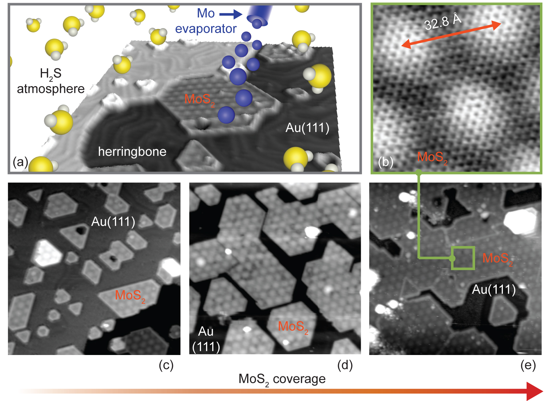
Detailed growth procedure of MoS2 on Au(111). The synthesis of SL MoS2 was performed in an UHV chamber (base pressure of 210-10 mbar) equipped with a home-built Aarhus-type scanning tunneling microscope (STM)Besenbacher et al. (1988). With this experimental set-up, each step of the entire growth process could be monitored. All STM images were acquired with an etched W tip, and the bias voltages stated in the Article refer to the voltage applied to the sample. The effect of instrumental artifacts, such as piezo creep, were minimized by calibrating the STM micrographs in the free WSxM software Horcas et al. (2007) to match the known lattice constant of MoS2 or the moiré periodicity of MoS2 on Au(111), previously established in the literature Sørensen et al. (2014). The Au(111) sample was cleaned by repeated 2 keV Ar+ sputtering and 850 K annealing cycles, and the cleanliness of the surface was verified by the presence of the Au herringbone reconstruction by STM. The synthesis was initiated by backfilling the chamber with H2S gas to a pressure of 10-7 mbar using a custom-made doser with the end of the nozzle (4 mm diameter) placed about 1 mm away from the sample surface to increase the local pressure of impinging H2S gas Lauritsen and Besenbacher (2006). Inside the stainless steel nozzle an approximately 3 cm long capillary with a diameter of 40 m was mounted to constrict the flow of H2S from a high pressure reservoir to a high vacuum system. In this H2S atmosphere and with the sample held at room temperature, metallic Mo was deposited onto the sample surface using a commercially available e-beam evaporator (EGCO4, Oxford Instruments). The deposition rate in our experiment was calibrated by a separate deposition of Mo onto a clean Au(111) surface and was found to be 0.08 ML/minute; this deposition rate was used throughout the experiment. After a 5 minute Mo deposition, the H2S atmosphere was maintained while the sample was annealed to 850 K for 30 minutes. Once the sample reached a temperature of 450 K during the subsequent cooling, the H2S gas flow was stopped and the gas was pumped out of the chamber. These two steps – i.e Mo deposition and anneal, which both take place in the H2S environment – constitute one growth cycle. The first growth cycle yields a coverage of up to 0.3 ML. We note that during the anneal step some of the deposited Mo may have alloyed with the Au crystal thereby reducing the expected MoS2 coverage per growth cycle Christensen et al. (1997). The growth cycle is repeated until an almost continuous coverage of SL MoS2 is obtained, each cycle increasing the overall size of the MoS2 islands. We were unable to achieve high quality SL MoS2 beyond a coverage of 0.3 ML without cycling the growth process. A single long Mo deposition in H2S only produced low quality sub-ML films. Furthermore, cooling the sample to 300 K between each cycle appeared to promote the growth of high quality films. With this synthesis method, the MoS2 coverage can be easily tuned to accommodate the experiment or application at hand.
We found that once a coverage of 0.8 ML was reached, regions of BL MoS2 began to seed and form. Increasing the number of growth cycles produced more and larger islands of BL MoS2, whose subsequent growth and evolution were similar to the growth and evolution of SL MoS2; however, the contours of the BL MoS2 islands were noticeably more irregular compared to the SL MoS2 islands at a similar coverage.
Angle-resolved photoemission and low energy electron diffraction measurements. Angle-resolved photoemission spectroscopy (ARPES) measurements were performed at the SGM-3 beamline Hoffmann et al. (2004) at the ASTRID2 synchrotron radiation source. A photon energy of 70 eV was used to measure the electronic band structure of SL and BL MoS2, as this energy showed the strongest enhancement of the layer-dependent changes in the electronic states Miwa et al. (2015a). The energy and momentum resolution were 25 meV and 0.02 Å-1, respectively. Low energy electron diffraction (LEED) patterns were acquired for MoS2-covered and clean Au(111) surfaces using a LEED optics mounted on the ARPES analysis chamber. The base pressure in the analysis chamber was in the low 10-10 mbar regime, and the sample temperature was held at 70 K for the duration of the measurements.
III Results and Discussion
The synthesis of large-area SL MoS2 has been systematically explored by varying the Mo deposition rate, H2S pressure and dose, sample temperature and annealing time. Overall we find that the successful synthesis of high-quality extended SL MoS2 is strongly affected by two opposing effects concerned with the solubility of Mo in Au (alloy formation) and the diffusivity of Mo species on the surface. Both effects are strongly influenced by the sample temperature, but the deposition in H2S serves to strongly suppress the alloy formation due to the reaction between the Mo and S, as well as the binding between S and Au. When the Mo deposition is carried out in a 10-7 mbar H2S atmosphere and subsequently post-annealed at a relatively low temperature (673 K), the result is a very well-defined array of triangular MoS2 nanoparticles as reported in Ref. Helveg et al. (2000) . This interesting MoS2 morphology is attributed to a relatively low mobility of Mo at this temperature and the fact that nucleation of Mo predominantly occurs at the elbows of the characteristic Au(111) herringbone reconstruction Barth et al. (1990), yielding extended ordered arrays of amorphous Mo clusters on the surface. The higher post-anneal temperature of 850 K used here for a duration of 30 minutes in the H2S environment increases the mobility of Mo on the surface and promotes the growth of SL MoS2 islands that are tens of nanometers in sizeSørensen et al. (2014). Alloying of Mo and Au at these elevated temperatures would be very severe, but the effect is strongly reduced due to the presence of the H2S atmosphere. Choosing this set of experimental parameters leads to relatively large MoS2 islands with truncated triangular and hexagonal shapes on the Au(111) surface as observed in the STM image in Fig. 1(c). Such islands are oriented with the (0001) basal plane of MoS2 parallel to the Au surface and are seen to be distributed over the entire Au surface, which in this case reflects a total SL MoS2 coverage of 0.3 ML. The high resolution STM image of the area marked by the green square in Fig. 1(e) reveals the atomically resolved lattice and the moiré structure of MoS2. The incommensurability of the Au lattice (lattice constant of 2.88 Å) and MoS2 lattice (3.15 Å) gives rise to a moiré structure that manifests itself on the (0001) basal planes of MoS2 as clearly visible protrusions in a hexagonal pattern with a periodicity of 32.8 Å (denoted by the double-headed orange arrow in Fig. 1(b)). Further attempts to increase the size of these islands by increasing the Mo coverage did not lead to a more uniform SL MoS2 coverage and it was not possible to increase the annealing temperatures above 850 K due to severe alloying of the Mo and Au that occurs irrespective of the H2S pressure. Instead of increasing the temperature and Mo coverage in one step, the key to increasing the coverage of high quality SL MoS2 involves repeated cycles of Mo evaporation and annealing in H2S, using the aforementioned conditions. This results in islands merging together at a MoS2 coverage of 0.6 ML as shown in Fig. 1(d). Continued cycling of the growth process leads to a further increase in coverage (0.8 ML) and the formation of a nearly contiguous SL of MoS2, see Fig. 1(e).
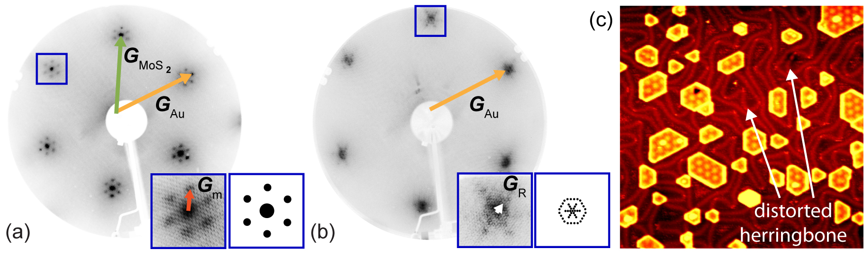
The structural details of the 0.8 ML coverage MoS2 sample are studied by STM in Fig. 1(b) and (e) and by LEED in Fig. 2(a). A sharp hexagonal diffraction pattern with satellites surrounding each main diffraction spot is observed, suggesting a clean, ordered and extended SL of MoS2. The satellite spots are consistent with the moiré pattern observed in the STM images, indicating a large-area presence of this pattern. To highlight the origin of each diffraction spot, we have added reciprocal lattice vectors in Fig. 2(a). G points to the main diffraction spots corresponding to the MoS2 lattice while the satellites are associated with the moiré reciprocal lattice vector, Gm, as well as the Au(111) reciprocal lattice vector GAu. A separate LEED image of the clean Au(111) surface is shown for comparison in Fig. 2(b). The structure and diffraction pattern of the Au(111) surface reconstruction is well-established Barth et al. (1990); Huang et al. (1990); Sandy et al. (1991); Hove et al. (1981), but we summarize it here to facilitate a comparison with the diffraction pattern of the MoS2 adlayer. The LEED image of Au(111), acquired at 300 K, also exhibits a sharp hexagonal diffraction pattern with accompanying hexagonally positioned satellite features because of the rectangular 22 Au reconstructed unit cell which encompasses both face-centered cubic (fcc) and hexagonal close-packed (hcp) regions that arise from an average 4.55 compression of the first layer along the [10] directions of the bulk truncated surface Barth et al. (1990); Iski et al. (2012). Ridges form between the two different close-packed regions, creating a chevron or herringbone superstructure with 120∘ rotational symmetry. The implications of this superstructure are a multitude of extra spots amongst the satellite spots Huang et al. (1990); Sandy et al. (1991). As seen in the insets of Fig. 2(b), these extra spots define the outer contour of the small hexagon and radiate out along spokes from its center. The hexagonal arrangement of the satellite spots for the clean Au(111), compared to the high coverage MoS2 sample, are rotated with respect to one another by 30 ∘ – see insets of Fig. 2(a) and (b) – indicating that the satellite features from the clean Au sample result from the herringbone surface reconstruction while the satellite features for the high coverage MoS2 sample are instead due to the moiré (i.e. the interaction between the MoS2 and the underlying Au). The reciprocal lattice vector for the reconstructed Au(111) surface, GR, is shown in the inset of Fig. 2(b) and the magnitude of the vector is scaled with respect to Gm in the corresponding inset of Fig. 2(a). We note that higher order spots associated with the Au herringbone structure are also visible in the LEED pattern of Fig. 2(b). Since both diffraction patterns are acquired using electrons with a kinetic energy of 114 eV, the absence of the Au satellite features in the high coverage MoS2 LEED data of Fig. 2(a) strongly suggests that the herringbone reconstruction is lifted upon addition of the MoS2 adlayer. These same Au spots are absent in LEED measurements of the MoS2 sample acquired at different kinetic energies. Such a lifting of the reconstruction is not surprising as there are numerous reported instances of the addition of adatoms and adlayers leading to a redistribution of substrate surface atoms; for example, small species such as H, CO, H2S and O2 will perturb the peculiar quasi-hexagonal reconstruction of Pt(001) Ulstrup et al. (2013); Nilsson et al. (2012), and self-assembled networks of oxygen- and sulphur-containing molecules can partially or fully lift the herringbone reconstruction of Au(111) Iski et al. (2012); Gatti et al. (2014); Jewell et al. (2010); Poirier and Pylant (1996); Poirier (1997); Sørensen et al. (2014). Indirect evidence of this lifting is seen for a small number of MoS2 islands that appear brighter than the rest and still display a moiré pattern, such as the brighter island in Fig. 1(c). This increase in apparent height is exactly consistent with the 2.3 Å height of an extra layer of Au atoms beneath the SL MoS2 island Jewell et al. (2010). Such small extra Au islands are expected to be generated by the lifting of the herringbone reconstruction, as this reconstruction has a higher density of atoms (4.5 ) in the first layer compared to the truncated bulk surface Poirier (1997). The lifting of the native Au reconstruction is also supported by the STM image in Fig. 2(c) which shows triangular-loop-like distortions of the regular herringbone reconstruction even after only one MoS2 growth cycle. These perturbations are similar to previously reported STM data of Au thin films grown on Ru(0001) which suggest that such triangular-like structures are amenable to relieving strain in stacked hexagonal layers Ling et al. (2006).
The STM images also reveal the presence of distinct line defects, as shown in Fig. 3(a). These line defects are boundaries between two opposite rotational domains of the three-fold symmetric MoS2 lattice on the unreconstructed Au(111) surface lattice. Similar line defects have been observed in scanning transmission electron microscopy measurements of CVD-grown MoS2 on SiO2 Zhou et al. (2013). The MoS2 islands are either terminated in the 100 or (010) directions. These terminations are referred to as the Mo-edge and S-edge, respectively. Joining islands with the same domain orientation – which is equivalent to the meeting of two different edge types – will result in the formation of a continuous SL of MoS2. However, structural domain boundaries arise when domains of differently oriented MoS2, or correspondingly the same edge types, meet during the growth process as shown in Fig. 3.
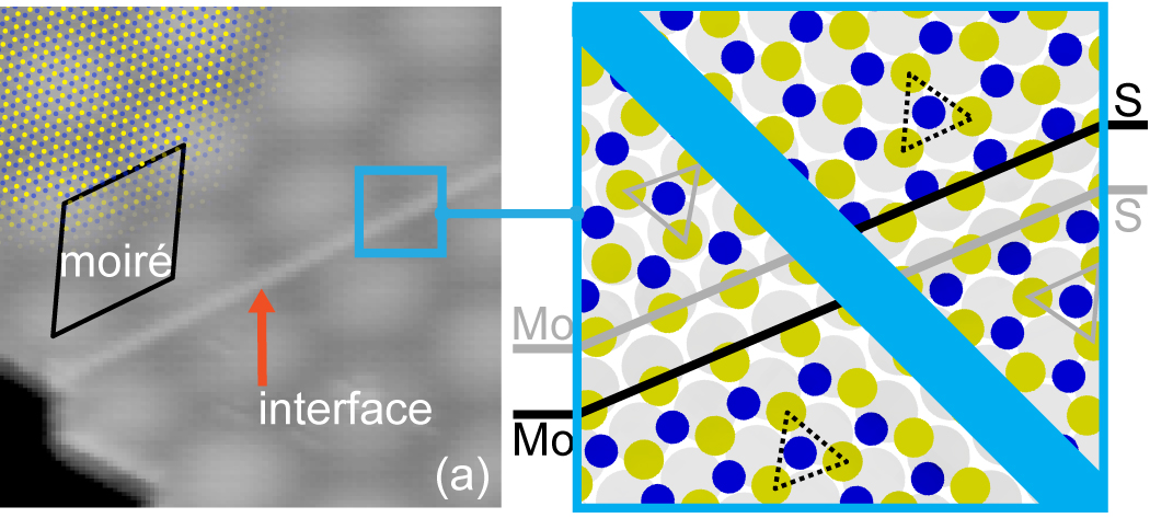
It is not clear from the STM images which type of interface is present for each individual line defect as only the upper layer of S atoms is imaged by STM Kobayashi and Yamauchi (1995). Hence both possible interfaces are shown in Fig. 3(b) separated by a light blue line. The 60∘ rotational domains are neither expected to influence the LEED pattern (although they would affect the relative spot intensities), nor would they have an effect on the overall electronic structure of SL MoS2 due to the hexagonal symmetry of the reciprocal lattice. However, the presence of line defects suggests that domains rotated by 60∘ coexist in our sample, and this is of crucial importance as it implies that the high symmetry points and in the BZ from different rotational domains coincide in laterally averaging techniques such as ARPES.
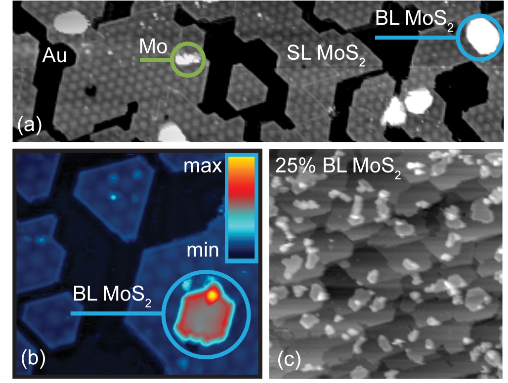
Our STM images of the high coverage SL MoS2 films frequently reveal additional features atop SL MoS2, which are evident from Fig. 4. We assign the irregularly shaped clusters highlighted by the green circle in Fig. 4(a) to amorphous Mo clusters, which may result from insufficient sulfurization during the growth cycles. Perhaps more interesting is the feature marked by the blue circle, which shows the formation of a BL MoS2 island. A STM image of such an island is shown in Fig. 4(b). In contrast to the SL islands, the basal plane of the BL appears flat in the center of the island; a moiré is absent and it is difficult to obtain atomic resolution. The apparent height of the BL islands relative to the underlying SL islands is Å. This value is comparable to the bulk inter-layer spacing of 6.15 Å in the 2H-stacking of S-Mo-S layers, supporting the assignment of these features to BL and not multilayer islands.
As the number of growth cycles is increased, we foster the formation of more and larger islands of BL MoS2. In the STM image shown in Fig. 4(c), the BL regions appear brighter than the surrounding darker SL MoS2 film. Upon close inspection of the STM image, the SL MoS2 still manifests a moiré pattern that is unaffected by the presence of the BL MoS2 islands. Here, the BL MoS2 covers an estimated 25 of the surface. The contours of the BL MoS2 islands are notably more irregularly shaped than SL MoS2 islands for a similar coverage; see Fig. 1(c) for comparison. Such irregular contours have been observed for SL MoS2 islands grown on highly ordered pyrolytic graphite Kibsgaard et al. (2006) and more recently on graphene Miwa et al. (2015a), where the adlayer-substrate interaction is governed by van der Waals forces. Given that, in BL regions, the interaction between the second layer of the BL MoS2 and the underlying SL MoS2 film is weaker than the interaction between the SL MoS2 and the underlying Au substrate, we might expect to see growth of islands with many different rotational domains orientations. This tendency to form various rotational domains of BL MoS2, together with the irregular shapes of the BL islands, suggests that such islands may not seamlessly merge together during subsequent growth cycles and will indeed make the synthesis of large domains of high quality multilayers of MoS2 challenging.
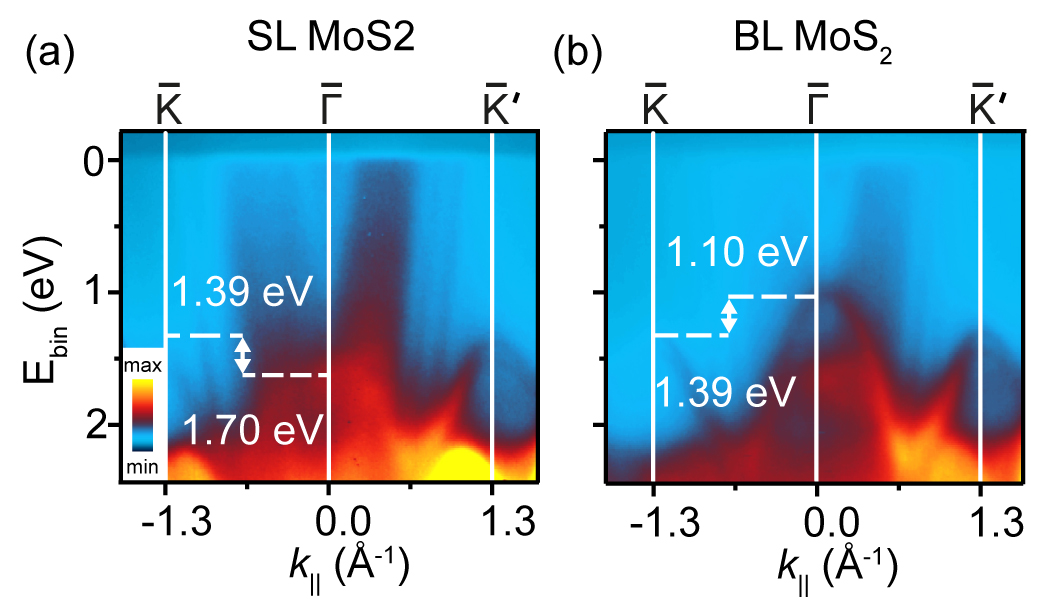
We carried out electronic structure measurements by ARPES of both the SL and BL MoS2 samples in order to compare their band structures on Au(111). The detailed features of SL MoS2 on Au(111) in ARPES are discussed in Ref. Miwa et al. (2015b). Here we focus on the VB dispersion along the – – direction of the MoS2 BZ as shown in Fig. 5. For SL MoS2 the global VB maximum is situated at the -point, which resides within the projected band gap of the Au electronic structure. Consequently the electronic states of MoS2 in this region of the BZ do not interact with the Au bulk states, and the MoS2 bands appear sharp and well-defined Takeuchi et al. (1991). The upper VB at exhibits a spin splitting with a measurable separation of (1454) meV Miwa et al. (2015b). The top of the VB at falls within the continuum of projected Au bulk states. The broad character of these VB states is attributed to their interaction with the Au bulk states Zhu et al. (2011); Cappelluti et al. (2013); Miwa et al. (2015b). This observation is in contrast to ARPES data acquired for SL MoS2 grown on graphene where the MoS2 band structure is completely unperturbed by the substrate Miwa et al. (2015a).
The most pronounced difference between the ARPES measurements of the SL and BL MoS2 samples is the binding energy position of the VB maximum at . The binding energy differences with respect to are highlighted by the dashed white lines along with the salient binding energy, , values. For SL MoS2, the VB at exhibits a local maximum at a binding energy of 1.70 eV, which is 0.31 eV below the VB global maximum (1.39 eV) at . This picture is consistent with the view that SL MoS2 is a direct band gap semiconductor. With ARPES only the occupied states of a material are probed, so this expectation cannot be immediately and directly verified. However it has been previously shown that by alkali doping SL MoS2 on Au(111), the conduction band minimum can be sufficiently occupied such that this direct band gap at can be measured Miwa et al. (2015b). For BL MoS2 an extra dispersing band appears around at 1.10 eV or 0.29 eV above the position of the VB local maximum at . (The positions of the VB maxima are determined from fits of the energy distribution curves which are not shown here but the method has been previously demonstrated for SL MoS2 Miwa et al. (2015b).) For BL MoS2 the appearance of two distinct bands at (Fig. 5a) arises from an interaction between the two MoS2 layers, leading to the formation of a bonding/anti-bonding splitting of the VB Cheiwchanchamnangij and Lambrecht (2012). This is a very distinct spectral feature of the BL case, and in contrast to SL MoS2 (Fig. 5a) where the splitting of the bands at the VB maximum situated at is purely a spin-orbit effect due to a lack of inversion symmetry in the TMDC Zhu et al. (2011). In fact, the direct to indirect band gap transition arising from additional interlayer interactions has recently been observed in optical spectroscopy measurements of MoS2 samples with thicknesses ranging from one to six layers Mak et al. (2010) and MoSe2 with thicknesses up to eight layers Zhang et al. (2014b). Furthermore, the MoS2 bands around for BL MoS2 appear a lot sharper and narrower than the bands near for the SL case, something we ascribe to the increased interaction between the two layers rather than the hybridization of just a single adlayer with the underlying Au substrate. This is consistent with the appearance of the BL MoS2 islands in STM, where they appear to be very weakly interacting with the substrate.
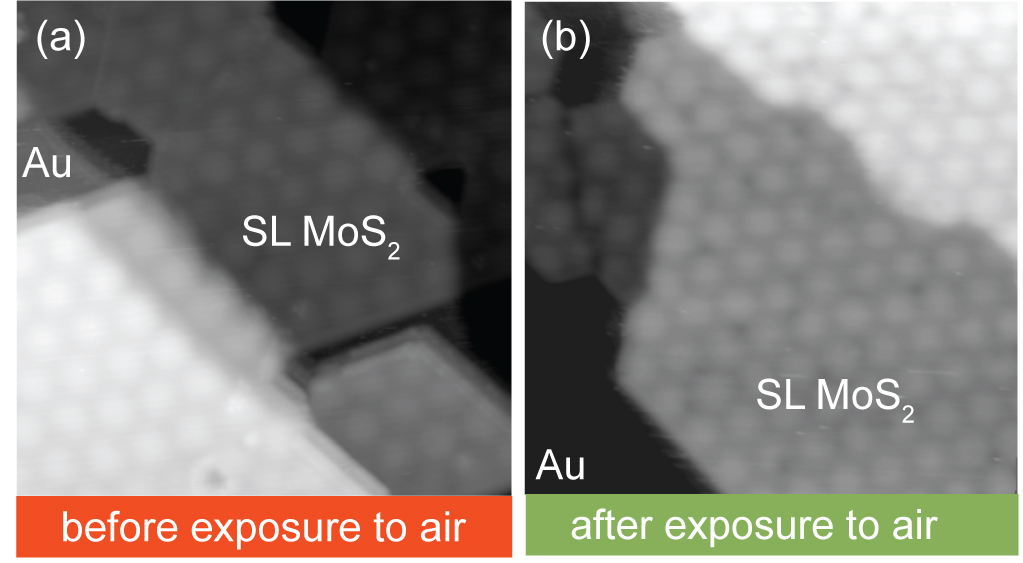
The chemical stability of our epitaxial SL MoS2 samples towards air exposure is tested as shown in Fig. 6. The STM images present the SL MoS2 lattice before (a) and after (b) air exposure at room temperature for a few hours, followed by a mild annealing to 500 K in UHV to remove physisorbed species. Incidentally, these SLs appear to be stable up to even higher anneal temperatures of approximately 900 K. Prolonged exposure to air, i.e. in excess of several hours, can lead to extensive accumulation of adsorbates, and these higher annealing temperatures are generally found to be more effective for cleaning the sample. The quality of the surfaces in the images is essentially identical, demonstrating the chemical robustness of the epitaxial SL MoS2 on Au(111). This result suggests an inert character of these SL MoS2 samples towards an oxidizing gas – a property which greatly simplifies the transfer of samples between different experimental set-ups.
IV Conclusions
We have developed a procedure for synthesizing large area epitaxial SL MoS2 on Au(111), and demonstrated that these samples are robust against exposure to air. We expect this UHV compatible growth method to further surface sensitive characterization studies and nanoscale device applications that may require larger areas of SL MoS2 than those typically achieved by mechanical exfoliation. Moreover, a comparison of the ARPES data obtained from MoS2 layers grown with this method Miwa et al. (2015b) to those from exfoliated samples Jin et al. (2013) suggest that the former may be of superior quality. Our MoS2 synthesis method is based on cycles of Mo evaporation and sulfurization to gradually increase the coverage of SL MoS2 and avoid excessive formation of amorphous Mo clusters and BL MoS2 islands. The MoS2 layer seems to be comprised of domains rotated by 60∘ which lead to the formation of straight line defects at domain boundaries. Upon comparison with LEED data of a clean Au(111) sample we find that the native herringbone reconstruction of Au is lifted with the addition of the MoS2 adlayer. This controlled growth method of epitaxial SL MoS2 should be transferable to similar TMDCs and other substrates as long as the interaction between the TMDCs and the surface is strong enough to seed initial island growth and prohibit the formation of random domain orientations. Rotational domains could be avoided by choosing surface orientations of reduced symmetry.
V Acknowledgement
We gratefully acknowledge financial support from the VILLUM foundation, the Danish Council for Independent Research, Natural Sciences under the Sapere Aude program (Grant Nos. DFF-4090-00125 and DFF-4002-00029), the Lundbeck Foundation, the Danish Strategic Research Council (CAT-C) and Haldor Topsøe A/S.
References
- Geim and Grigorieva (2013) A. K. Geim and I. V. Grigorieva, Nature 499, 419 (2013).
- Novoselov et al. (2005) K. S. Novoselov, D. Jiang, F. Schedin, T. J. Booth, V. V. Khotkevich, S. V. Morozov, and A. K. Geim, PNAS 102, 10451 (2005).
- Butler et al. (2013) S. Z. Butler, S. M. Hollen, L. Cao, Y. Cui, J. A. Gupta, H. R. Gutiérrez, T. F. Heinz, S. S. Hong, J. Huang, A. F. Ismach, et al., ACS Nano 7, 2898 (2013).
- Rao et al. (2014) C. Rao, U. Maitra, and U. V. Waghmare, Chemical Physics Letters 609, 172 (2014).
- Bradley et al. (2015) A. J. Bradley, M. M. Ugeda, F. H. da Jornada, D. Y. Qiu, W. Ruan, Y. Zhang, S. Wickenburg, A. Riss, J. Lu, S.-K. Mo, et al., Nano Letters 15, 2594 (2015).
- Mak et al. (2010) K. F. Mak, C. Lee, J. Hone, J. Shan, and T. F. Heinz, Phys. Rev. Lett. 105, 136805 (2010).
- Splendiani et al. (2010) A. Splendiani, L. Sun, Y. Zhang, T. Li, J. Kim, G. Chim C.-Y.and Galli, and F. Wang, Nano Lett. 10, 1271 (2010).
- Wang et al. (2012) Q. H. Wang, K. Kalantar-Zadeh, A. Kis, J. N. Coleman, and M. S. Strano, Nat. Nano. 7, 699 (2012).
- Rao et al. (2013) C. N. R. Rao, H. S. S. Ramakrishna Matte, and U. Maitra, Angewandte Chemie International Edition 52, 13162 (2013).
- Ramasubramaniam (2012) A. Ramasubramaniam, Phys. Rev. B 86, 115409 (2012).
- Ugeda et al. (2014) M. M. Ugeda, A. J. Bradley, S.-F. Shi, F. H. da Jornada, Y. Zhang, D. Y. Qiu, W. Ruan, S.-K. Mo, Z. Hussain, Z.-X. Shen, et al., Nat Mater 13, 1091 (2014).
- Xiao et al. (2012) D. Xiao, G.-B. Liu, W. Feng, X. Xu, and W. Yao, Phys. Rev. Lett. 108, 196802 (2012).
- Xu et al. (2014) X. Xu, W. Yao, D. Xiao, and T. F. Heinz, Nat. Phys. 10, 343 (2014).
- Zeng et al. (2012) H. Zeng, J. Dai, W. Yao, D. Xiao, and X. Cui, Nat. Nano. 7, 490 (2012).
- Zhang et al. (2014a) Y. J. Zhang, T. Oka, R. Suzuki, J. T. Ye, and Y. Iwasa, Science 344, 725 (2014a).
- Mak et al. (2012) K. F. Mak, K. He, J. Shan, and T. F. Heinz, Nat. Nano. 7, 494 (2012).
- Helveg et al. (2000) S. Helveg, J. V. Lauritsen, E. Lægsgaard, I. Stensgaard, J. K. Nørskov, B. S. Clausen, H. Topsøe, and F. Besenbacher, Phys. Rev. Lett. 84, 951 (2000).
- Füchtbauer et al. (2013) H. G. Füchtbauer, A. K. Tuxen, P. G. Moses, H. Topsøe, F. Besenbacher, and J. V. Lauritsen, PCCP 15, 15971 (2013).
- Radisavljevic et al. (2011) B. Radisavljevic, A. Radenovic, J. Brivio, V. Giacometti, and A. Kis, Nat. Nano. 6, 147 (2011).
- Cao et al. (2012) T. Cao, G. Wang, W. Han, H. Ye, C. Zhu, J. Shi, Q. Niu, P. Tan, E. Wang, B. Liu, et al., Nat. Comm. 3, 887 (2012).
- Shi et al. (2012) Y. Shi, W. Zhou, A.-Y. Lu, W. Fang, Y.-H. Lee, A. L. Hsu, S. M. Kim, K. K. Kim, H. Y. Yang, L.-J. Li, et al., Nano Lett. 12, 2784 (2012).
- Kim et al. (2011) D. Kim, D. Sun, W. Lu, Z. Cheng, Y. Zhu, D. Le, T. S. Rahman, and B. Ludwig, Langmuir 27, 11650 (2011).
- Sørensen et al. (2014) S. G. Sørensen, H. G. Füchtbauer, A. K. Tuxen, A. S. Walton, and J. V. Lauritsen, ACS Nano 8, 6788 (2014).
- Besenbacher et al. (1988) F. Besenbacher, E. Laegsgaard, K. Mortensen, U. Nielsen, and I. Stensgaard, Rev. Sci. Instrum. 59, 1035 (1988).
- Horcas et al. (2007) I. Horcas, R. Fernández, J. M. Gómez-Rodríguez, J. Colchero, J. Gómez-Herrero, and A. M. Baro, Rev. Sci. Instrum. 78 (2007).
- Lauritsen and Besenbacher (2006) J. Lauritsen and F. Besenbacher (Academic Press, 2006), vol. 50 of Advances in Catalysis, pp. 97 – 147.
- Christensen et al. (1997) A. Christensen, A. V. Ruban, P. Stoltze, K. W. Jacobsen, H. L. Skriver, J. K. Nørskov, and F. Besenbacher, Phys. Rev. B 56, 5822 (1997).
- Hoffmann et al. (2004) S. Hoffmann, C. Søndergaard, C. Schultz, Z. Li, and P. Hofmann, Nuclear Instruments and Methods in Physics Research Section A: Accelerators, Spectrometers, Detectors and Associated Equipment 523, 441 (2004).
- Miwa et al. (2015a) J. A. Miwa, M. Dendzik, S. S. Grønborg, M. Bianchi, J. V. Lauritsen, P. Hofmann, and S. Ulstrup, ACS Nano 9, 6502 (2015a).
- Barth et al. (1990) J. V. Barth, H. Brune, G. Ertl, and R. J. Behm, Phys. Rev. B 42, 9307 (1990).
- Huang et al. (1990) K. G. Huang, D. Gibbs, D. M. Zehner, A. R. Sandy, and S. G. J. Mochrie, Phys. Rev. Lett. 65, 3313 (1990).
- Sandy et al. (1991) A. R. Sandy, S. G. J. Mochrie, D. M. Zehner, K. G. Huang, and D. Gibbs, Phys. Rev. B 43, 4667 (1991).
- Hove et al. (1981) M. V. Hove, R. Koestner, P. Stair, J. Bibérian, L. Kesmodel, I. BartoŠ, and G. Somorjai, Surface Science 103, 189 (1981).
- Iski et al. (2012) E. V. Iski, A. D. Jewell, H. L. Tierney, G. Kyriakou, and E. C. H. Sykes, Surface Science 606, 536 (2012).
- Ulstrup et al. (2013) S. Ulstrup, L. Nilsson, J. A. Miwa, R. Balog, M. Bianchi, L. Hornekær, and P. Hofmann, Physical Review B 88, 125425 (2013).
- Nilsson et al. (2012) L. Nilsson, M. Andersen, R. Balog, E. Lægsgaard, P. Hofmann, F. Besenbacher, B. Hammer, I. Stensgaard, and L. Hornekær, ACS Nano 6, 10258 (2012).
- Gatti et al. (2014) R. Gatti, J. M. MacLeod, J. A. Lipton-Duffin, A. G. Moiseev, D. F. Perepichka, and F. Rosei, The Journal of Physical Chemistry C 118, 25505 (2014).
- Jewell et al. (2010) A. D. Jewell, H. L. Tierney, and E. C. H. Sykes, Physical Review B 82, 205401 (2010).
- Poirier and Pylant (1996) G. E. Poirier and E. D. Pylant, Science 272, 1145 (1996).
- Poirier (1997) G. E. Poirier, Chemical Reviews 97, 1117 (1997).
- Ling et al. (2006) W. Ling, J. Hamilton, K. Thürmer, G. Thayer, J. de la Figuera, R. Hwang, C. Carter, N. Bartelt, and K. McCarty, Surface Science 600, 1735 (2006).
- Zhou et al. (2013) W. Zhou, X. Zou, S. Najmaei, Z. Liu, Y. Shi, J. Kong, J. Lou, P. M. Ajayan, B. I. Yakobson, and J.-C. Idrobo, Nano Lett. 13, 2615 (2013).
- Kobayashi and Yamauchi (1995) K. Kobayashi and J. Yamauchi, Phys. Rev. B 51, 17085 (1995).
- Kibsgaard et al. (2006) J. Kibsgaard, J. V. Lauritsen, E. Lægsgaard, B. S. Clausen, H. Topsøe, and F. Besenbacher, Journal of the American Chemical Society 128, 13950 (2006).
- Miwa et al. (2015b) J. A. Miwa, S. Ulstrup, S. G. Sørensen, M. Dendzik, A. Grubišić Čabo, M. Bianchi, J. V. Lauritsen, and P. Hofmann, Phys. Rev. Lett. 114, 046802 (2015b).
- Takeuchi et al. (1991) N. Takeuchi, C. T. Chan, and K. M. Ho, Phys. Rev. B 43, 13899 (1991).
- Zhu et al. (2011) Z. Y. Zhu, Y. C. Cheng, and U. Schwingenschlögl, Phys. Rev. B 84, 153402 (2011).
- Cappelluti et al. (2013) E. Cappelluti, R. Roldán, J. A. Silva-Guillén, P. Ordejón, and F. Guinea, Phys. Rev. B 88, 075409 (2013).
- Cheiwchanchamnangij and Lambrecht (2012) T. Cheiwchanchamnangij and W. R. L. Lambrecht, Phys. Rev. B 85, 205302 (2012).
- Zhang et al. (2014b) Y. Zhang, T.-R. Chang, B. Zhou, Y.-T. Cui, H. Yan, Z. Liu, F. Schmitt, J. Lee, R. Moore, Y. Chen, et al., Nat. Nano. 9, 111 (2014b).
- Jin et al. (2013) W. Jin, P.-C. Yeh, N. Zaki, D. Zhang, J. T. Sadowski, A. Al-Mahboob, A. M. van der Zande, D. A. Chenet, J. I. Dadap, I. P. Herman, et al., Phys. Rev. Lett. 111, 106801 (2013)..