Concurrent conductance and transition voltage spectroscopy study of scanning tunneling microscopy vacuum junctions. Does it unravel new physics? ∗†
Ioan Bâldea a‡
Published: RSC Advances 2014, 4, 33257-33261; DOI: 10.1039/C4RA04648J
Abstract:
We show that the conductance () and transition voltage () spectroscopy data for standard vacuum nanogaps reported in the preceding paper by Sotthewes et al cannot be understood within the framework of the existing theories/models whatever realistic effects are incorporates. However, if we include an additional (“ghost”) current, the trends of the dependencies of and on the nanogap size can be explained. The ghost current is very small. Therefore, effects related to the ghost current can only be revealed at larger ’s, where the ghost current becomes comparable to or overcomes the tunneling current. Although we are not able to unravel the origin of this ghost contribution, we can and do refer to experimental - and -data reported for molecular junctions, which exhibit similarities to the presently considered vacuum nanojunctions. Analyzing notable difficulties related to the regime assigned as transport via hopping, we speculate that a ghost contribution may also exist in molecular junctions.
Keywords: nanoelectronics; nanotransport; vacuum STM junctions; transition voltage spectroscopy
1 Introduction
A long standing challenge in the field of molecular electronics is whether the measured currents are really mediated by the active molecules intentionally embedded in the nanodevice under consideration or are (also) significantly affected, e.g., by impurities or defects.1, 2 From this perspective, the transport through vacuum nanodevices seems to be privileged, because it is hard to imagine how could the measured current be plagued by undesired “ghost” channels giving rise to a current overimposed on the current due to the tunneling across the vacuum nanogap. However strange it might be, after ruling out all causes we could conceive, we have to conclude that the challenging experimental results on the transition voltage spectroscopy (TVS) 3, 1 reported in the preceding paper 4 cannot be explained without assuming a “ghost” contribution. The origin of such a transport channel contributing to the transport in standard vacuo remains the big mystery, which the present work cannot unravel. Still, what we can presently do is to point out to some similarities with results reported for molecular junctions 5, 6, 7 and suggest that a similar contribution can also be present there.
2 Theoretical details
The tunneling current through a vacuum nanogap can be determined by exact numerical solution of the Schrödinger equation by using a tunneling barrier that includes contribution from the applied bias , electrodes’ (STM substrate and tip ) work functions , and image charges 8, 9
| (1) | |||||
| (2) |
The “bare” rectangular barrier due the electrodes’ work function is tilted by the applied bias and reduced by (classical) image charges . For two planar electrodes, the exact expression of 8 can be used to numerically find the exact transmission coefficient 10, 11.
In the discussion that follows we will assume that, besides the current due to electron tunneling through a metal-vacuum-metal junction in a scanning tunneling microscope (STM) setup, the measured current also comprises a “ghost” current (cf. 1)
| (3) |
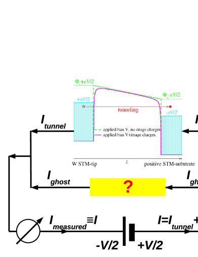
For simplicity, we will assume that the latter represents an Ohmic contribution, that is,
| (4) |
Here is the applied bias between the STM tip and substrate, which are spatially separated by a vacuum nanogap of size , and stands for the ghost (average) resistivity.
Below, we will focus our attention on the Ohmic conductance and the transition voltage . is defined as the bias at the minimum of the Fowler-Nordheim quantity 3, or, equivalently, by the point where the differential conductance is two times larger than the pseudo-Ohmic conductance 12. The interplay between the tunneling and ghost contributions of eqn (3) will be characterized by the dimensionless quantity related to the ghost resistivity
| (5) |
3 Results
3.1 Attempting to incorporate realistic effects into the tunneling barrier
The results for presented in Fig. 1 and 5 of ref. 4, showing that calculations based on Simmons-type approximation, similar to those done earlier 13, 14, cannot explain the -dependence of the transition voltage found in experiment (cf. Fig. 4A and 4B of ref. 4) may not be surprising; shortcomings of the Simmons approach to transition voltage spectroscopy are amply documented 9, 10, 15.
In the first part of the present analysis, we will show that the tunneling transport model cannot explain the experimental -data even when the numerical exact solution of the Schrödinger equation is employed (this is the case for all results presented here), and even attempting to make the barrier model more realistic. This is shown by the results presented in Fig. S1 of the ESI†, which emerged from the attempt to make the tunneling barrier as realistic as possible. (Throughout, labels S refer to the ESI†.)
Fig. 2a shows the effect of the difference between the STM-tip and substrate work functions ( eV versus eV or eV, respectively, cf. eqn (1). This may be important, because it yields an extra Volta-type field of a strength V/nm comparable to the applied field 8, 16, 11. As seen in Fig. 2a, the asymmetry semi-quantitatively explains the small difference between positive and negative biases for Pt substrates. As noted 4, the Shockley surface state, not included in the present calculations, represents a plausible source for the considerably larger asymmetry for Au (111) substrates. Fig. S1a demonstrates that image effects, which may be important at smaller sizes 16, are not essential for the -values used in experiments 4. The same figure indicates that the potential profile has no significant impact on (cf. Fig. S1a). Instead of well defined - and -values, it might be more realistic to consider statistical distributions of these quantities. These distributions may better model STM-tips without a well defined facet and polycrystalline Pt substrates. But, as visible in Fig. S1b and S1c, these effects do not improve the agreement with experiment.
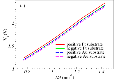
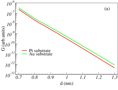
Fig. 2b depicts results for the Ohmic conductance , a quantity that also plays an important part in the subsequent analysis. Whatever the effects considered (cf. Fig S2), it does not notably deviate from the well-known exponential decay. This is also at variance with the experimental -data, which evolve to a plateau at larger -values (cf. Figure 4C of ref. 4).
3.2 Impact of a ghost current
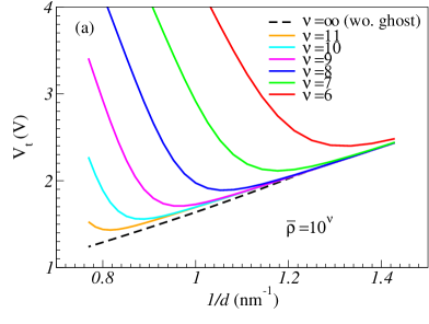
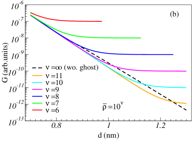
Let us now assume that a ghost current [eqn (4)] exists, and examine its impact on and . Results for and at various values of the parameter are presented in Fig. 3a and Fig. 3b. The trend observed in these figures is compatible with the experimental behavior.
In the plateau regime ( nm), experiments found S for platinum substrates and S for gold substrates (cf. Figure 4C of ref. 4). A reliable estimate for the transverse area vacuum nanogap depends, amongst others, on the actual tip shape and cannot be given 18. So, let us assume a tip radius nm. Inserting the above values in eqn (5), we get for Au and for Pt. These estimates fall in the -range employed in Fig. 3, wherein the increase of with predicted by the conventional theory switches to the decrease observed in experiments 4. So, a ghost current may be at the origin of both Ohmic conductances saturating at larger ’s and transition voltages that decrease with . We have checked that this trend is not affected if the realistic effects discussed in the preceding subsection and the ESI† are included in calculations.
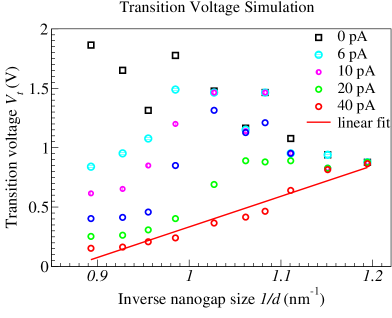
As a supplementary test related to the most unexpected experimental finding of ref. 4 (namely, a decreasing with ), we present further results in Fig. 4. The black squares shown there are experimental data vs. . The other symbols depicted in Fig. 4 correspond to obtained by subtracted from the experimental curves a (ghost) current proportional to [cf. eqn (4)], which has been gradually increased from cyan-magenta-blue-green to red circles (-values are indicated in the legend). In spite of certain scattering in the data, the trend is pretty clear: the data switch from a decreasing with to a increasing with . The differences between the red circles and the red line (linear fit of the red circles) of Fig. 4 are within the experimental errors. We assign the last curve (red circles) as a situation where the ghost current has been eliminated. So, what remained is the genuine tunneling current, and the corresponding curve (red points) behaves like the curves found in Fig. 2a within the conventional theory, wherein merely the tunneling current has been accounted for. The red circles correspond to a ghost resistance G. Assuming again tip radii nm, we find , which is compatible with the range covered in Fig. 3.
To end this section, we note that neither the - nor the -dependence of the ghost current assumed in eqn (4) is critical for the behavior depicted in Fig. 3. To check the impact of the -dependence of eqn (4), we performed calculations by using a -independent ghost resistance and found no significant modification. Likewise, to check the impact of the -dependence, instead of the contribution of eqn (4), we added a small constant term to the transmission across the tunneling barrier [i.e., using in eqn (S1)]. Results obtained in this way, which are presented in Fig. S3, do not qualitatively differ from those of Fig. 3. Notice that this procedure — which amounts to consider a “ghost” transmission channel, a pseudo-diffusion or hopping — yields via eqn (S1) a nonlinear ghost current. To summarize the results based on further functional dependencies studied, we can state that the qualitative behavior depicted in Fig. 3 holds provided that the - and -dependencies of the ghost current are much weaker than the corresponding (exponential) dependencies of the tunneling current.
4 Discussion
We have shown above that the experimental data for electron transport in STM vacuum junctions can be rationalized by postulating the existence of a ghost current. What could be the origin of the ghost current? A imperfect electric insulation cannot come in question 18. The vacuum in experiments is very good ( mbar); therefore it is very unlikely that a conduction channel through the vacuum junction is responsible for the ghost currents needed in Fig. 3 and Fig. 4. To rule out a ghost current flowing through the electronic circuit, the experimentalists have checked that for large tip-sample separation ( nm) the measured current is negligible 18. A small DC offset voltage of the converter gives an unavoidable, small contribution ( pA) to the measured current, which should be independent on the bias; however, any residual offset current has been subtracted before processing the data 18. Therefore, this possibility should also be ruled out.
So, we are unable to unravel the origin of the ghost current postulated above (even, see below) in a standard vacuum nanogap. Still, we believe that this issue may be related to pieces of experimental work on molecular junctions of two independent groups. Some time ago, Frisbie’s group first reported a crossover between two different transport regimes in molecular junctions employing the conducting probe atomic force microscopy (CP-AFM) setup 5, 6. For shorter molecules, the resistance was found temperature () independent and increasing exponentially with increasing length (), in contrast to longer molecules characterized by an Arrhenius -dependence and a linear -dependence. Extracting information on single-molecules using transport data on CP-AFM junctions 5, 6, comprising many () molecules, might be not straightforward. A subsequent work of Tao’s group 7 on single-molecule STM-junctions confirmed the crossover between two transport regimes with the same signatures noted above 5, 6. Fully in light with current understanding of charge transport, these - and -dependencies have been taken as clear evidence of charge transport via tunneling in shorter molecules and via hopping in longer molecules 5, 6, 7.
While by no means intending to challenge that, with increasing , tunneling becomes less effective and hopping increasingly important, for reasons exposed below we believe that this is not the whole issue related to the transport data of refs. 5, 6, and 7. Particularly problematic to us appear the very large values of the activation energies extracted from experiments, an aspect on which ref. 6 already drew attention. As discussed in the ESI†, ref. 6 drastically overestimated the reorganization energies , because the contributions of all intramolecular vibrations were included in calculations; in reality, only very low frequency modes, which can be thermally activated, can contribute 19. Even though, the (over)estimated -values remain several times smaller than those needed to explain the large experimental activation energies . The measured values eV 6 and eV 7 would require enormous reorganization energies eV [cf. eqn (S5)] hardly compatible with known (including author’s) results of quantum chemical calculations.
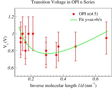
The -dependence of the resistance of the aforementioned experimental works on molecular junctions 5, 6, 7 is similar to the presently considered vacuum nanojunctions (compare Figure 2A of ref. 5, Figure 6b of ref. 6, and Figure 3 of ref. 7 with Figure 4C of ref. 4 and the present Fig. 3b). This represents one important fact for the present analysis, but not the only one. In addition to results for vs. , ref. 5 reported results on for oligophenyleneimines (OPIs) of various sizes. Interestingly, the trend visible in Fig. 5, wherein these results are depicted, resembles the trend of Fig. 3a. So, it is tempting to interpret the similarity between the -dependence of Fig. 5 and Fig. 3a as suggesting that a ghost current may also exist in molecular junctions.
5 Conclusion
TVS was initially proposed as a tool of extracting the energy offset of the dominant frontier orbital relative to electrode’s Fermi energy in molecular junctions 3, and a series of studies 21, 12, 22, 17 demonstrates that it holds its promise. The fact that can be used to quantify a significant nonlinear transport 12 makes TVS a method of interest even beyond molecular electronics, and ref. 4 as well as the present paper have illustrate its utility for vacuum nanojunctions.
We have shown that the conductance and TVS data for a standard vacuum nanogap reported in ref. 4 cannot be understood within the framework of the existing theories/models whatever realistic effects are incorporates. However, if we include an additional (“ghost”) current, the experimental trends vs. and vs. exhibited by the Ohmic conductance and transition voltage can be explained. The ghost current is very small; it could not have played a significant role in ref. 14 because at the very small nanogap sizes employed there ( nm 14) the tunneling current is too large, and it masks a possible ghost contribution. Effects related to the ghost current can only be revealed at larger nanogap sizes (like those of ref. 4), where the ghost current overcomes the tunneling current. This is the reason why we believe that incorporating electrodes’ atomistic structure (e.g., within approaches based on the density functional theory 23, 24) will not change the conclusions of the present study, which is mostly based on the classical barrier picture for charge transport via tunneling in vacuo. Such details can be quite relevant for TVS in other cases: e.g., for vacuum nanogaps of sizes smaller than those ( nm) presently considered 23, or molecular junctions 24, where through-space processes are negligible.
The analysis of existing studies on size-dependence of and in molecular junctions have indicated that a ghost current may also be present in those nanosystems, which could have a significant role in properly assessing and characterizing the transport mechanism (e.g. hopping). From this perspective, investigating the impact of temperature on in the non-exponential -dependent regime is a possible topic of further experimental work. Another subject of experimental investigation could be the shot noise. Puzzling, although shot noise is a concept put forward in the context of vacuum tubes 25, we are not aware of shot noise studies in vacuum nanogaps. Such studies may provide supplementary information. Both and sample information contained in the -characteristic (expressed via the first power of the transmission coefficient ), while also comprises information on the second power ; in addition, at relatively large biases , samples information on a broader energy range around the Fermi energy, as pointed out recently 19.
To end, we have to admit that we are unable to unravel the origin of this mysterious ghost current that seems to be present even in a standard vacuum nanogap. However speculative this idea might seem — a fact of which we are fully aware—, we believe that the experimental support presented here in favor of a presently unknown (“ghost”) transport channel can represent a sufficient justification for considering the scenario proposed here a working hypothesis, which deserves further investigations. Nanoelectronics could be the main beneficiary.
Acknowledgment
The author thanks Prof. Harold Zandvliet for providing him with
the data of his group prior to publication and numerous valuable
experimental details and comments.
Financial support provided by the Deutsche Forschungsgemeinschaft
(grant BA 1799/2-1) is gratefully acknowledged.
Notes and references
- Kushmerick 2009 J. Kushmerick, Nature, 2009, 462, 994–995.
- Song et al. 2011 H. Song, M. A. Reed and T. Lee, Adv. Mater., 2011, 23, 1583–1608.
- Beebe et al. 2006 J. M. Beebe, B. Kim, J. W. Gadzuk, C. D. Frisbie and J. G. Kushmerick, Phys. Rev. Lett., 2006, 97, 026801.
- 4 K. Sotthewes, C. Hellenthal, A. Kumar and H. J. M. Zandvliet, RSC Adv., DOI 10.1039/C4RA04651J.
- Choi et al. 2008 S. H. Choi, B. Kim and C. D. Frisbie, Science, 2008, 320, 1482–1486.
- Choi et al. 2010 S. H. Choi, C. Risko, M. C. R. Delgado, B. Kim, J.-L. Bredas and C. D. Frisbie, J. Amer Chem. Soc., 2010, 132, 4358 – 4368.
- Hines et al. 2010 T. Hines, I. Diez-Perez, J. Hihath, H. Liu, Z.-S. Wang, J. Zhao, G. Zhou, K. Müllen and N. Tao, J. Am. Chem. Soc., 2010, 132, 11658–11664.
- Sommerfeld and Bethe 1933 A. Sommerfeld and H. Bethe, Handbuch der Physik, Julius-Springer-Verlag, Berlin, 1933, vol. 24 (2), p. 446.
- Bâldea and Köppel 2012 I. Bâldea and H. Köppel, Phys. Lett. A, 2012, 376, 1472 – 1476.
- Bâldea 2012 I. Bâldea, Europhys. Lett., 2012, 98, 17010.
- Bâldea and Köppel 2012 I. Bâldea and H. Köppel, Phys. Stat. Solidi (b), 2012, 249, 1791–1804.
- Bâldea 2012 I. Bâldea, Chem. Phys., 2012, 400, 65–71.
- Huisman et al. 2009 E. H. Huisman, C. M. Guédon, B. J. van Wees and S. J. van der Molen, Nano Lett., 2009, 9, 3909– 3913.
- Trouwborst et al. 2011 M. L. Trouwborst, C. A. Martin, R. H. M. Smit, C. M. Guédon, T. A. Baart, S. J. van der Molen and J. M. van Ruitenbeek, Nano Lett., 2011, 11, 614–617.
- Bâldea 2012 I. Bâldea, J. Phys. Chem. Solids, 2012, 73, 1151 – 1153.
- Gundlach 1966 K. H. Gundlach, Solid-State Electronics, 1966, 9, 949 – 957.
- Bâldea 2013 I. Bâldea, Nanoscale, 2013, 5, 9222–9230.
- Zandvliet private communication H. J. W. Zandvliet, private communication.
- Bâldea 2014 I. Bâldea, J. Phys. Chem. C, 2014, 118, 8676–8684.
- Guo et al. 2011 S. Guo, J. Hihath, I. Diez-Pérez and N. Tao, J. Am. Chem. Soc., 2011, 133, 19189–19197.
- Bâldea 2012 I. Bâldea, Phys. Rev. B, 2012, 85, 035442.
- Bâldea 2012 I. Bâldea, J. Am. Chem. Soc., 2012, 134, 7958–7962.
- Wu et al. 2013 K. Wu, M. Bai, S. Sanvito and S. Hou, Nanotechnology, 2013, 24, 025203.
- Wu et al. 2013 K. Wu, M. Bai, S. Sanvito and S. Hou, J. Chem. Phys., 2013, 139, 194703.
- Schottky 1918 W. Schottky, Annalen der Physik, 1918, 362, 541–567.