High frequency electro-optic measurement of strained silicon racetrack resonators
Abstract
The observation of the electro-optic effect in strained silicon waveguides has been considered as a direct manifestation of an induced non-linearity in the material. In this work, we perform high frequency measurements on strained silicon racetrack resonators. Strain is controlled by a mechanical deformation of the waveguide. It is shown that any optical modulation vanishes independently of the applied strain when the applied voltage varies much faster than the carrier effective lifetime, and that the DC modulation is also largely independent of the applied strain. This demonstrates that plasma carrier dispersion is responsible for the observed electro-optic effect. After normalizing out free carrier effects, our results set an upper limit of to the induced high-speed tensor element at an applied stress of . This upper limit is about one order of magnitude lower than the previously reported values for static electro-optic measurements.
In the last years, a lot of effort was spent investigating the strain induced second order nonlinearity ( effect) in Silicon by investigating the induced Pockels effect jacobsen ; chim ; chim2 ; puckett ; pedro . Strain induced could be instrumental to make ultrafast and energy efficient electro-optic modulators for the Silicon photonics platform which would replace present electro-optic modulators based on the plasma dispersion effect reed ; vivien ; xu ; Liu . More generally, the presence of an appreciable in Silicon would validate the Silicon-on-Insulator (SOI) platform as an alternative to Lithium Niobate for second order nonlinear optics cazza ; mher . In most of these works, the centro-symmetry of Silicon is broken by a stressing film of Silicon Nitride which induces strain in the underlying Silicon waveguide and enables a - at least from a first principle point of view Costanza . With the exception of refs. cazza ; mher , the Pockels effect was investigated by using an integrated imbalanced Mach-Zehnder interferometer in which one or both interferometer arms are driven by a DC or a low frequency () AC electric field jacobsen ; chim ; chim2 ; puckett ; pedro . Then, an effective value is extracted from the measured shift of the interference fringes by taking into account the system geometry and the magnitude of the applied static electric field. As expected from theory, the relation between the effective index change and the applied static electric field is found to be linear. The linear relation between these two physical quantities is considered as the evidence of the observation of a Pockels effect. Unfortunately, a linear effective index variation of the optical mode of a waveguide can also be induced by free carriers azadeh ; rajat or by trap states and localized charges at the SiNx-Si interface azadeh ; mher . A definitive proof of the strain induced non-linearity can be obtained by high frequency measurements in an interferometer structure since the Pockels effect and the free carrier dispersion are characterized by two different characteristic times. In this letter, we measure the separate contributions to the effective of the Pockels effect and of the plasma dispersion effect. We investigate the frequency response of the electro-optic effect in a racetrack resonator up to , i.e., well above the effective free carrier lifetime in the waveguide. In particular, by using a dedicated setup, we were able to tune continuously the strain in a same device so as to verify accurately how the applied strain modifies the system’s frequency response.
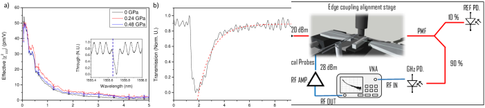
Our test structure is shown in fig.1(a). It consists of a racetrack resonator in the Add-Drop filter configuration Masi fabricated on a 6” SOI wafer. The resonator has a perimeter of and a coupling coefficient with the bus waveguide of . A thick LPCVD Silicon Nitride () layer is conformally deposited on the silicon waveguide. We use a thick Buried Oxide Layer (BOX) and a thick Silica layer as lower and upper cladding materials. The residual stress on the layer has been measured to be . An electric field can be applied in the z direction (see fig.1(a)) using three Aluminum electrodes along a straight waveguide section. With reference to the geometry shown in fig.1(a), this is achieved by grounding the central electrode on the top of the waveguide, and by shorting the two adjacent electrodes to a common voltage. This configuration is similar to the one reported in ref. pedro . The waveguide width changes adiabatically from outside the electrode region to below them. The waveguide height is kept fixed at . Using the adiabatic tapers, we are able to probe the electro-optic modulation in the wide multimode waveguide by preserving the fundamental mode excitation. As shown in fig.1(b), the device is fixed on a sample holder which can provide a variable stress adjusted by rotating a pitch screw. The material strain is mechanically induced by fixing the sample ends to the holder and by subsequently bending its center by means of the pressure exercised by the screw. We found that it is possible to displace the screw by approximately its complete pitch before breaking the chip. To avoid micro fractures, we kept screw displacements lower than . It is important to note that, with respect to other studies in which the analysis is performed by comparing samples with different strain jacobsen ; chim ; chim2 ; puckett ; pedro ; cazza ; mher , in our case it is possible to tune continuously the induced strain in the very same sample/resonator. As indicated in fig. 1(c), light from a C-band infra-red laser amplified by an Erbium Doped Fiber Amplifier (EDFA) is edge coupled to the Input port of the resonator using a Polarization Maintaining Lensed Fiber (PMF). The light polarization is set to Transverse Magnetic (TM). A nanometric XYZ positioning stage is used to minimize the coupling losses. The transmitted light from the resonator Through port is split: is sent to a reference photodiode, while feeds a high bandwidth photoreceiver () connected to a Vector Network Analyzer (VNA). The VNA also provides (after amplification) of sinusoidal voltage modulation to the electrodes using impedance matched Tungsten tips with a bandwidth.
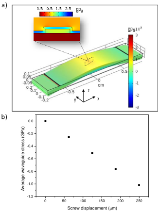
We determined the relation between the screw displacement and the stress induced inside the waveguide from Finite Element Method (FEM) computations. The results are shown in fig.2(a-b). Only the element of the stress tensor is plotted, since it is found to be one order of magnitude higher than the component and five orders of magnitude higher than the remaining tensor elements. In the region where the resonator is located (dashed rectangle in fig. 2(a)), the overall stress distribution can be approximated as compressive and uniaxial in the direction. In fig.2(b), we show a linear relation between the screw displacement and the computed average stress in the waveguide. At our working point (displacement ), the stress level is about in the waveguide and in the layer. The stress magnitude and direction is comparable to the ones used in other experiments jacobsen ; chim ; chim2 ; puckett ; pedro ; cazza ; mher . In the inset of fig. 2(a) we also notice that a high stress (hence strain) gradient is present at the upper and lower interfaces between and the waveguide. This feature is essential since it is theoretically predicted that the induced is proportional to the strain gradient in the material Costanza ; cazza .
At first, we set the screw displacement to zero, so no stress (except the residual one due to the interface) is applied to the waveguide.
By monitoring the output signal at the reference photodiode (fig. 1(c)), we tune the laser wavelength near the point of one of the resonances (fig. 3 (a) inset), where the sensitivity to small refractive index variations is maximized. The quality factor of this resonance is . We then apply a sinusoidal voltage to the sample electrodes (fig. 1 (a)) using the VNA and a electrical amplifier. As a result of the bias modulation, the resonance oscillates back and forth with respect to the laser wavelength, inducing a periodic modulation of the transmitted optical signal at the Through port of the resonator, similarly to the operation of a conventional resonant ring modulator (RRM). Assuming that this signal modulation is due to the electro-optic effect caused by the strain induced second order nonlinearity, the oscillation amplitude is given by:
| (1) |
in which is the local slope of the spectrum, is one of the resonance wavelengths of the resonator, is the length of region where the voltage is applied, is the resonator length, the refractive index of the core material of the waveguide and the average electric field in the core (computed using FEM simulations and assumed completely polarized in the direction). In Eq.1, the effective is defined as:
| (2) |
where is the local strain induced in the material, the refractive index distribution and the electric field of the optical mode. In Eq.2, we have assumed that the optical field is mainly polarized in the direction, so that off-diagonal tensor elements do not contribute to the integral. Eq.1 can be derived from the fact that the Pockels induced effective index change shifts the resonance frequency by a quantity . The VNA actually records , from which, through Eq.1, we extract
Figure 3(a) shows the effective values as a function of the driving bias frequency.
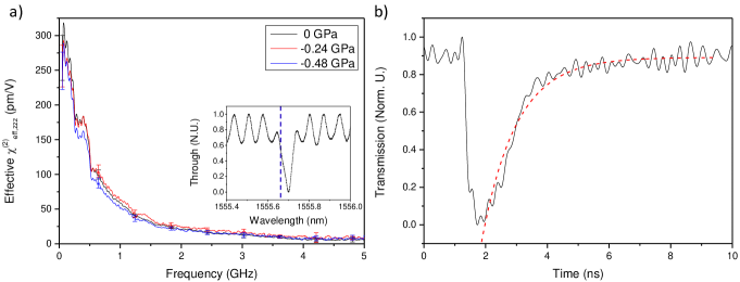
The latter is swept from to . As we can see, the value of is maximum in the low frequency range, and decreases as the modulation frequency increases. We point out that the extracted value close to DC regime is , which is comparable to values reported in the literature for static electro-optic measurements using the same electric field and optical polarization directions chim2 ; puckett . The cut-off frequency, i.e, the frequency at which the halves, is , corresponding to a time constant . The minimum value of that can be detected is limited by the electrical noise floor of the VNA and of the photoreceiver. This corresponds to an effective of . From fig. 3(a), one can see that this value is reached for . To exclude the possibility that the bandwidth is limited by the photon lifetime in the cavity, we modulated the optical input, and measured the signal at the Drop port with the laser wavelength tuned to the cavity resonance. The signal drops by from to , showing that the cavity is far from the optical cut-off. This frequency response has been subtracted from the curves in fig.3(a).
As shown in fig.3(a), we repeated the electro-optic measurements after applying stress levels to the waveguide of respectively and . Very slight differences are observed with respect to the no-stress case. We also tested waveguides with smaller widths, such as and , and found smaller transmission signal modulations compared to the wide one.
These results clearly show that the modulation can not be attributed to a strain induced , i.e., to the linear electro-optic effect. In fact, if the latter were the cause for the observed effect, one would expect the transmitted signal to follow voltage variations instantaneously up to optical frequencies. The signal modulation is rather related to a slower dispersion mechanism, with a characteristic time in the nanosecond scale. It has been recently shown that the plasma carrier dispersion effect can result in a linear electro-optic modulation if a charge layer is present at the interface azadeh ; rajat . Therefore, we checked the effective carrier lifetime in our waveguide to verify its consistency with the cut-off frequency in the electro-optic experiments. We used a pump and probe scheme, in which an intense laser pulse is coupled to the waveguide and the time dependent losses of a weaker probe beam are monitored. The short pump pulse generates free carriers due to two-photon absorption (TPA), these free carriers in turn attenuate the probe signal due to free-carrier absorption. After switching off the pump laser, the probe beam transmission slowly recovers due to free carrier recombination or diffusion away from the spot of the pump laser. The effective free carrier lifetime can then be extracted from the time-resolved measurement of the recovering probe beam transmission. The result is shown in fig. 3(b). The sudden signal decrease is due to the pulse arrival and, consequently, to TPA carrier generation. The following slower signal recovery is due to the finite free carrier lifetime. From these data, we estimated a carrier lifetime of .
Being , we conclude that the observed modulation can be attributed to plasma carrier dispersion. As further support to our conclusions, we applied static DC voltages to the electrodes of the racetrack resonator. We swept from to and measured the spectral response at the Drop port as a function of the bias. We found that the maximum dropped signal monotonically decreases with voltage. At , the signal decreases by with respect to the zero bias condition. This behaviour confirms that the electro-optic modulation is actually induced by free carriers since it also introduces additional round trip lossess that would be unexpected in the case of strain induced Pockels effect. Furthermore, it is interesting to observe that the modulation frequency response is limited by the carrier lifetime.
A plausible explanation of our observations is the accumulation and release of carriers at the interfaces as a consequence of the applied voltages azadeh ; zhang ; alloatti .
In addition, we set an upper limit to the strain induced of at of applied stress. This value is about an order of magnitude lower than those extracted from DC measurements, as reported here and in the literature chim ; chim2 ; puckett ; pedro . At DC, we believe induced modulation to be completely masked by free carrier effects. We remark here that our results do not exclude the presence of a strain induced in Silicon. Indeed, there exist proofs of Second Harmonic Generation (SHG) in strained Silicon that intrinsically can not have an explanation purely relying on free carrier cazza ; mher ; Govorkov . These experiments revealed a value of up to for applied stress. Differences can be due to the fact that the tensor is dispersive, so its value at optical frequencies can be significantly different from the one measured at DC cazza . In addition, it has recently been shown that electrostatic fields at the interface can couple with the optical fields through nonlinearities, resulting in a Electric Field Second Harmonic Contribution (EFISH) mher . This may have altered and consequently increased the extracted values of the .
To summarize the results, in this work we demonstrate that a strong linear electro-optic effect is present in strained Silicon waveguides due to free carrier dispersion. A dedicated experimental set-up allows us to continuously tune the applied stress on a very same racetrack resonator. By performing high frequency measurements of the optical transmission under an AC electric field variation, we found that the electro-optic modulation vanishes as the modulation speed exceeds the free carrier lifetime. Thus, we evidenced a time response in the nanosecond range and, consequently, ruled out the potential strain induced as the origin of the modulation. We extract an upper limit of for the strain induced in Silicon waveguides, which corresponds to our minimum detectable signal. This value is more than one order of magnitude lower than the one reported in the low frequency regime in the literature, which allows us to conclude that free carriers are responsible for the observed behavior. Larger stress or different stressing materials than are needed to definitely prove the presence of the electro-optic effect in strained Silicon waveguides.
Acknowledgment. The authors acknowledge Mr.Saeed Sharif for the collaboration and useful discussions we had during the measurement sessions. G. Pucker and M. Ghulinyan acknowledge the support of the staff of MNF during device fabrication. This work has been supported by the SIQURO project financed by the Autonomous Provincia of Trento.
References
- (1) R.S. Jacobsen, K.N. Andersen, P.I. Borel, J.Fage-Pedersen, L. H. Frandsen, O. Hansen, M. Kristensen, A.V. Lavrinenko, G. Moulin, H. Ou, C. Peucheret, B. Zsigri, and A. Bjarklev, Nature, 441, 199-202, (2006).
- (2) B. Chmielak, C.Matheisen, C. Ripperda, J. Bolten, T. Wahlbrink, M. Waldow, and Heinrich Kurz, Opt. Express, 21, 25324-25332, (2013).
- (3) B. Chmielak, M.Waldow, C. Matheisen, C.Ripperda, J.Bolten, T. Wahlbrink, M. Nagel, F. Merget, and H. Kurz, Opt. Express, 19, 17212-17219, (2011).
- (4) M. W. Puckett, J. S. T. Smalley, M. Abashin, A. Grieco, and Y. Fainman, Opt. Letters, 39, 1693-1696, (2014).
- (5) P. Damas, X. Le Roux, D. Le Bourdais, E. Cassan, D. Marris-Morini, N. Izard, T. Maroutian, P. Lecoeur, and L. Vivien, Opt. Express, 22, 22095-22100, (2014).
- (6) G. T. Reed, G.Mashanovich, F. Y. Gardes and D.J. Thomson, Nature Phot., 4, 518-526, (2010).
- (7) M. Ziebell, D. Marris-Morini, G. Rasigade, J.M. Fedeli, P. Crozat, E. Cassan, D. Bouville, and L. Vivien, Opt. Express, 20, 10591-10596, (2012).
- (8) Q. Xu, B. Schmidt, S. Pradhan, and M.Lipson, Nature, 435, 325-327, (2005).
- (9) A. Liu, R. Jones, L. Liao, D. Samara-Rubio, D. Rubin, O. Cohen, R. Nicolaescu, and M.Paniccia, Nature, 427, 615-618, (2004).
- (10) M. Cazzanell, F. Bianco, E. Borga, G. Pucker, M. Ghulinyan, E. Degoli, E. Luppi, V. Véniard, S. Ossicini, D. Modotto, S. Wabnitz, R. Pierobon, and L. Pavesi, Nat. Mater., 11, 148-154, (2012).
- (11) C.Schriever, F.Bianco, M. Cazzanelli, M. Ghulinyan, C. Eisenschmidt, J. De Boor, A.Schmid, J. Heitmann, L.Pavesi, and J. Schilling, Adv. Opt. Mater., 3, 129-136, (2015).
- (12) C. Manganelli, P. Pintus, and C. Bonati., arXiv preprint, arXiv:1507.06589 (2015).
- (13) S. Azadeh, F. Merget, M.P. Nezhad, and J.Witzens, Opt. Lett., 40, 1877-1880, (2015).
- (14) R. Sharma, M. Puckett, H. Lin, F. Vallini, and Y. Fainman, Appl. Phys. Lett., 106, 241104 (2015).
- (15) M.Masi, R. Orobtchouk, F.Guofang, J.M. Fedeli and L. Pavesi, J. Lightwave Technol., 28, 3233-3242, (2010).
- (16) P. Zhang, E. Tevaarwerk, B.N. Park, D. E. Savage, G. K. Celler, I. Knezevic, P. G. Evans, M. A. Eriksson, and M. G. Lagally, Nature, 439, 703-706, (2006).
- (17) L. Alloatti, C. Koos, and J. Leuthold, Appl. Phys. Lett., 107, 031107 (2015)
- (18) S.V. Govorkov, V.I. Emelyanov, N.I. Koroteev, G.I. Petrov, I.L. Shumay, and V.V. Yakovlev, J. Opt. Soc. Am. B, 6, 1117-1124, (1989).