present address: ]Consejo Nacional de Investigaciones Científicas y Técnicas (CONICET), Buenos Aires, Argentina
Ballistic transport in graphene antidot lattices
Abstract
Graphene samples can have a very high carrier mobility if influences from the substrate and the environment are minimized. Embedding a graphene sheet into a heterostructure with hexagonal boron nitride (hBN) on both sides was shown to be a particularly efficient way of achieving a high bulk mobility Wang1DContacts . Nanopatterning graphene can add extra damage and drastically reduce sample mobility by edge disorder PhysRevLett.102.056403 ; PhysRevB.82.041413 ; PhysRevB.85.195432 . Preparing etched graphene nanostructures on top of an hBN substrate instead of SiO2 is no remedy, as transport characteristics are still dominated by edge roughness BischoffBNRibbons . Here we show that etching fully encapsulated graphene on the nanoscale is more gentle and the high mobility can be preserved. To this end, we prepared graphene antidot lattices PhysRevLett.66.2790 where we observe magnetotransport features stemming from ballistic transport. Due to the short lattice period in our samples we can also explore the boundary between the classical and the quantum transport regime.
pacs:
In single layer graphene the charge carriers are completely exposed to the environment, which limits their mobility. Placing graphene on hexagonal boron nitride (hBN) was shown to improve the carrier mobility Dean2010 , allowing the observation of ballistic transport or the fractional quantum Hall effect in bulk graphene Dean2011 . Recently, a dry stacking technique was introduced, which allows complete encapsulation of graphene into layers of hBN and excludes any contamination from process chemicals such as electron beam resist Wang1DContacts . To obtain graphene nanodevices, chemically prepared graphene nanostructures Jiao2009 ; Kosynkin2009 ; Cai2010 are a potential route for certain applications, however, the high flexibility of a top down patterning approach is extremely desirable. Graphene antidot lattices can help circumventing the problem of the missing band gap in transistor applications Bai2010 , and were even predicted to serve as the technological basis for spin qubits PhysRevLett.100.136804 . Clearly, for advanced graphene nanodevices, not only the bulk mobility has to be improved, but the nanopatterning has to be optimised.
Here we present experiments on graphene antidot lattices PhysRevLett.66.2790 ; Eroms2009 ; Shen2008 etched into hBN/graphene/hBN heterostructures with lattice periods going down to nm. Magnetotransport on those samples shows commensurability features stemming from ballistic orbits around one or several antidots. This allows us to prove that the high carrier mobility is preserved in the nanopatterning step even though the zero field resistance is dominated by scattering on the artificial nanopattern, giving an apparent reduction of the mobility. The small feature size of our samples also allows us to approach the region where the classical picture of cyclotron orbits no longer applies. This classical to quantum crossover is governed by the ratio between the Fermi wavelength of the carriers and the dimensions of the nanopattern.
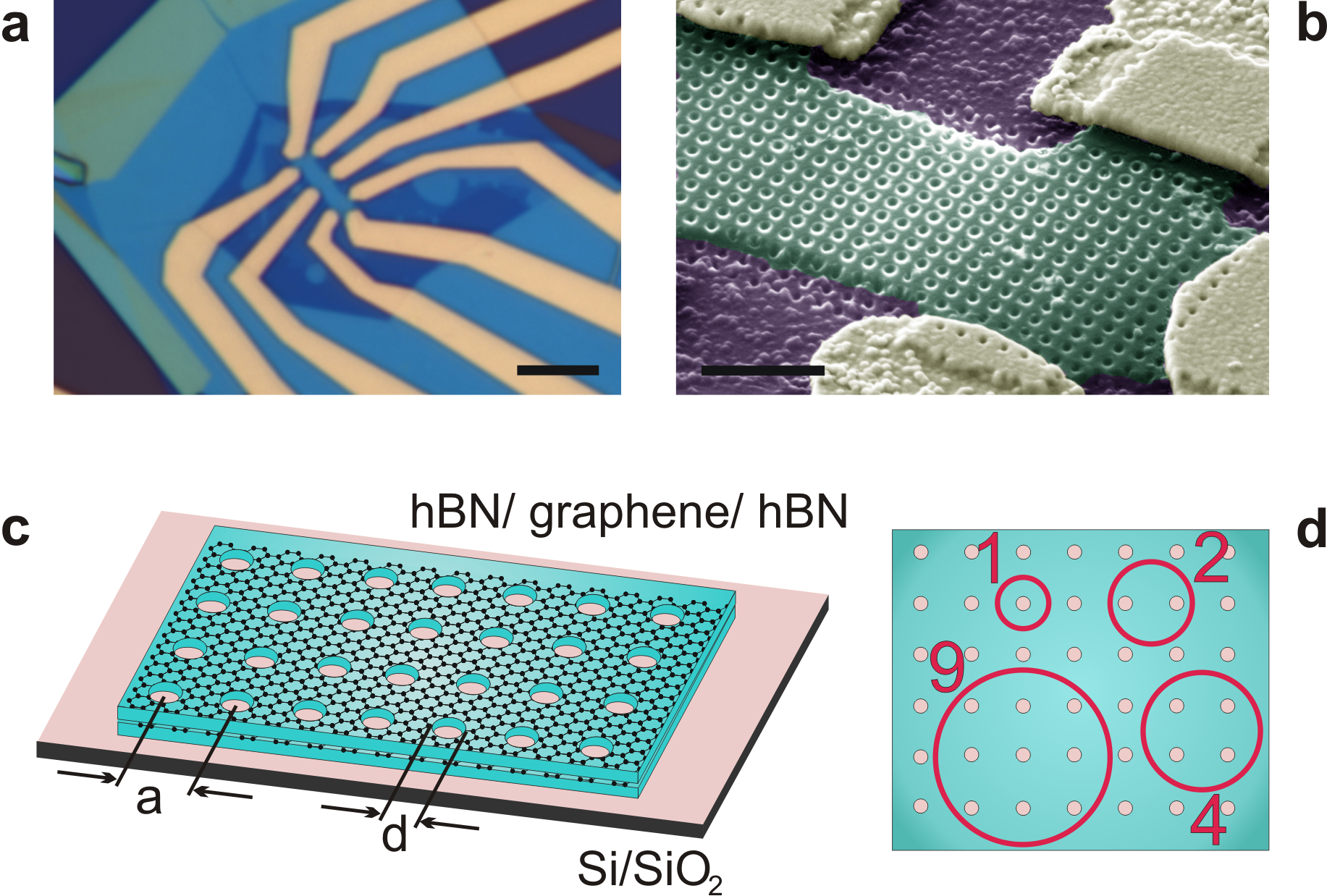
To obtain embedded graphene samples, hBN/graphene/hBN stacks were prepared using the dry stacking technique, patterned into Hall bar shape, and contacted using Cr/Au Wang1DContacts . In hBN/graphene/hBN samples prepared by this method, we routinely obtained carrier mobilities in excess of cm2/Vs, showing all integer quantum Hall states starting from a few Tesla. In one sample without antidots and a mobility of cm2/Vs we also observed the fractional quantum Hall effect at K. This shows that our fabrication procedure is mature and consistently yields high sample qualities. The samples presented in this study did not show any signs of a moiré superlattice Dean2013 ; GeimMoire . Afterwards, an antidot lattice was patterned. (For fabrication details, see Methods section). Fig. 1 shows an optical micrograph of a finished sample and a scanning electron micrograph of a sample after measuring. A sketch of the antidot lattice, etched into the stack is also shown. The antidot lattice period was varied between 50 nm and 250 nm. The antidot diameter was lithographically defined to be about 40 nm, but due to the conical etching profile, the actual diameter in the graphene plane is smaller. Using SEM inspection, we estimate it to be about nm.
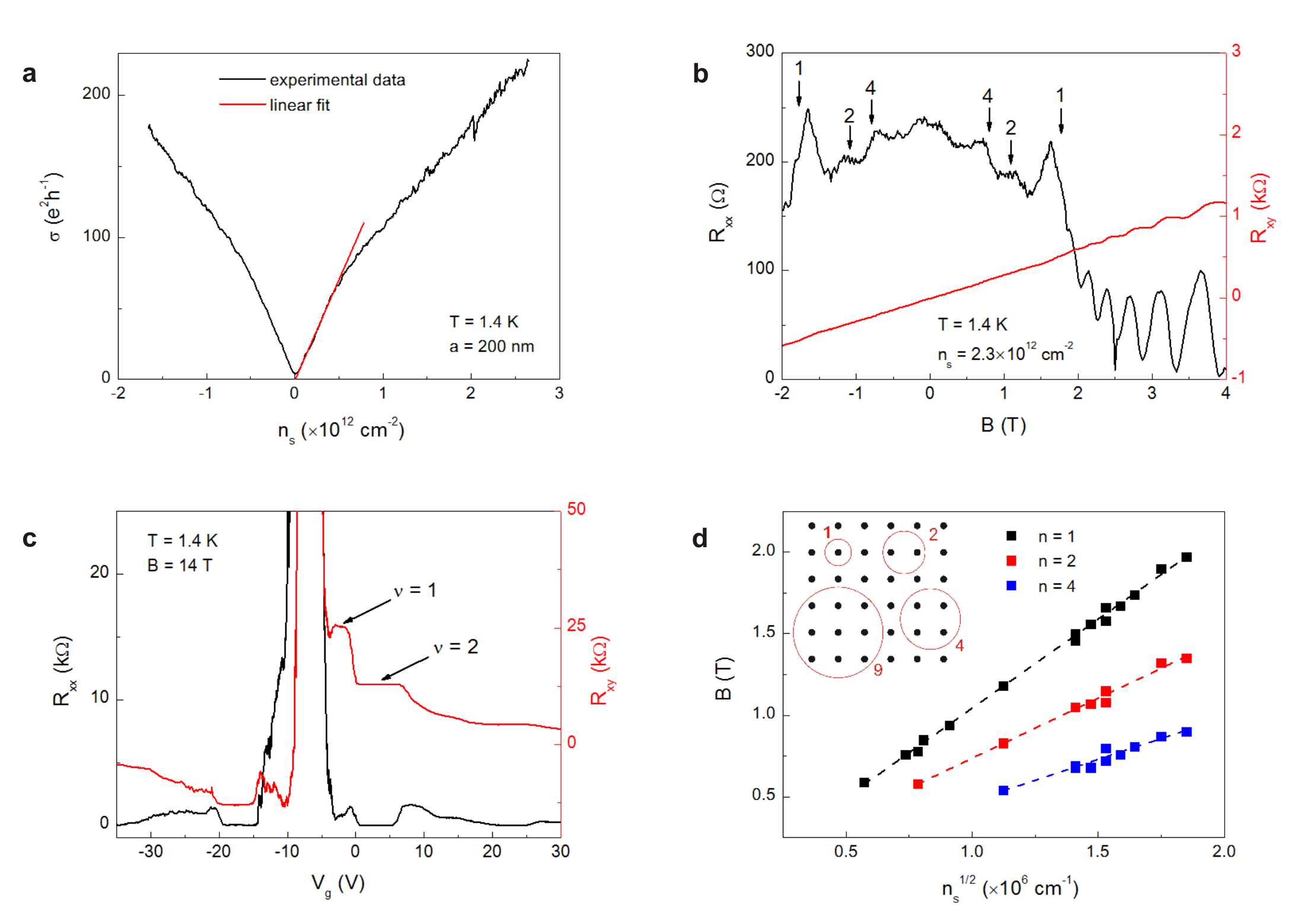
In Fig. 2, we show data for a sample with a lattice period of nm. From the gate response of the conductivity at a magnetic field , shown in Fig. 2a, we calculate an apparent field effect mobility of cm2/Vs. At a carrier density cm-2 this corresponds to an apparent mean free path of about nm. We estimate the intrinsic mean free path to be about 1400 nm Ishizaka1999 (see Supplementary Information). Magnetotransport traces of this device (see Fig. 2b) show pronounced peaks at field values where the cyclotron diameter is commensurate to the square antidot lattice. The peak belonging to , the fundamental antidot peak, is most pronounced. Additional peaks appearing at lower fields correspond to orbits encircling 2, and 4 antidots PhysRevLett.66.2790 (see Fig. 1d), confirming a mean free path which spans several lattice periods. While in a simple picture only the unperturbed orbits encircling the antidots are responsible for the magnetotransport features, a more detailed analysis based on the Kubo formula shows that velocity correlations in the chaotic trajectories, which occupy the largest part of the phase space, result in the magnetoresistance peaks PhysRevLett.68.1367 ; PhysRevB.55.16331 . Most of the orbits therefore hit the antidot edges several times within a mean free path. Hence, the visibility of the antidot peaks not only proves a high bulk mobility, but also shows that scattering at the edges does not cut off the trajectories and we can conclude that the high carrier mobility also survives after nanopatterning.
At higher fields, the cyclotron diameter is reduced below the neck width in between the antidots. We can observe Shubnikov-de Haas oscillations, eventually resulting in a well-defined quantum Hall effect. At T we clearly observe the plateau, which again shows the high sample quality (Fig. 2c). We evaluated the carrier density dependence of the magnetoresistance peaks corresponding to orbits around 1, 2 and 4 (Fig. 2d) and found that the peaks were always well described by a square root dependence of the cyclotron diameter on the carrier density down to cm-2. Quantitatively, we confirmed the formula for the cyclotron diameter for graphene given above, which contains spin and valley degeneracy.
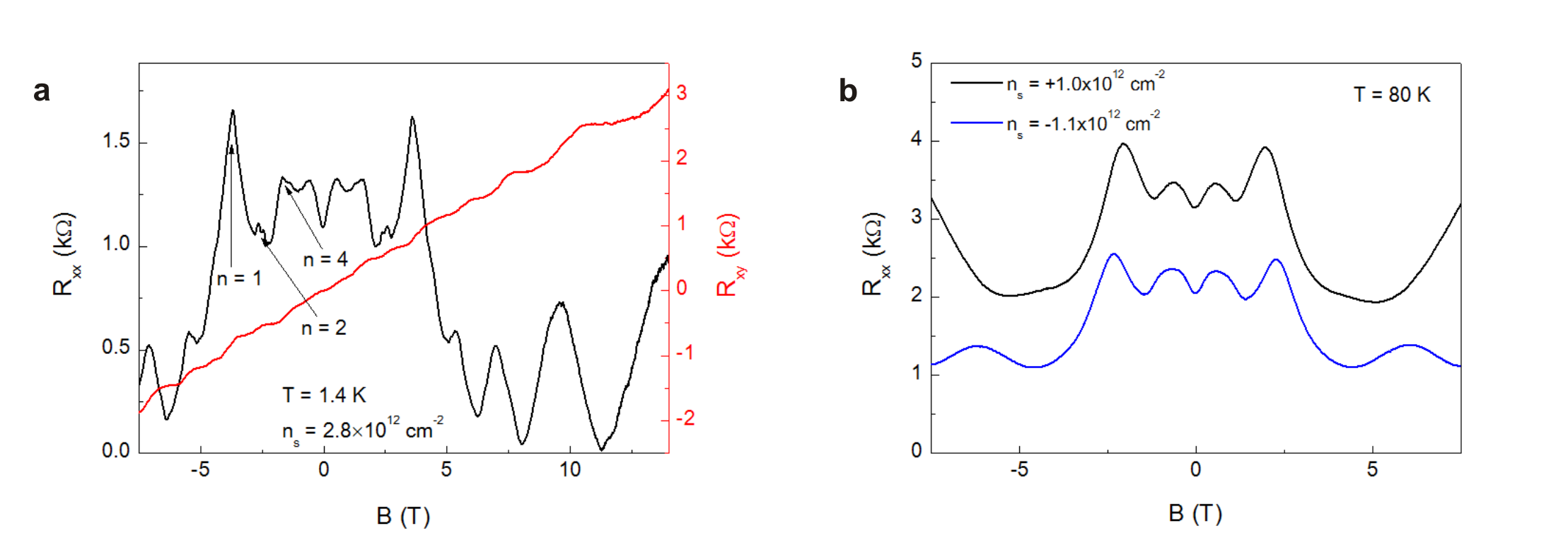
Fig. 3a shows the magnetoresistance of a sample with nm at cm-2. The apparent Hall mobility at this density is about cm2/Vs. Again, scattering at the antidot potential limits the apparent mobility Ishizaka1999 , but the intrinsic mobility is higher as we clearly observe magnetoresistance peaks for antidots, and a fourth peak at lower fields is weakly visible. Ishizaka and Ando studied how the visibility of the higher order antidot peaks depends on the mobility PhysRevB.55.16331 . From their data, we estimate that the intrinsic mean free path must be at least 400 nm, well in excess of the apparent mean free path of 160 nm (see Supplementary Information).
The good visibility of the peak confirms the small aspect ratio PhysRevB.55.16331 , in agreement with our SEM analysis and also with the onset of the well-defined Shubnikov-de Haas oscillations in our magnetotransport data. All these approaches give an antidot diameter of nm.
In experiments in GaAs based antidot lattices it was found that due to depletion at the antidot boundaries, the potential can be very soft and small lattice periods are hard to realize. In our case the data compares well to hard-wall potential lattices in GaAs, which could be realized in GaAs only at much larger lattice periods PhysRevLett.66.2790 . We also compared data for similar carrier densities in the electron and hole regime in Fig. 3b and found the graphs to be virtually identical. This proves that there is no edge doping at the antidot boundaries, which would have led to different potential shapes in the electron and hole regime due to Fermi level pinning at the edges.
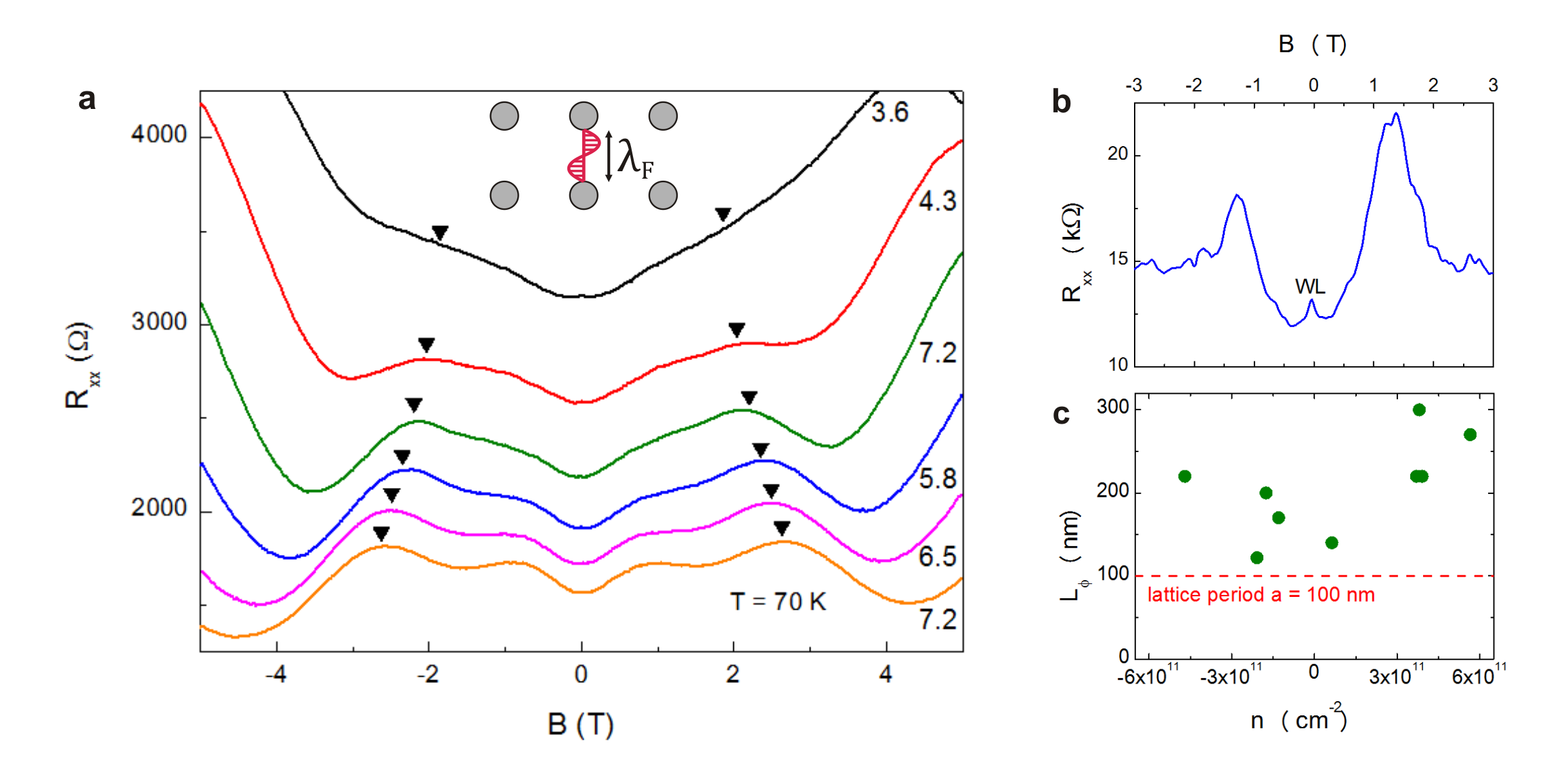
Now let us discuss the transition between the quantum and the classical transport regime. In GaAs-based heterostructures, the smallest lattice period realised so far was nm, and required critical tuning of the etch depth Antidots80nm . In contrast, due to the lack of a depletion region in graphene the fabrication of samples with a very small lattice period is less critical, and the carrier density is widely tunable. Also, due to valley degeneracy, the Fermi wavelength in graphene, is a factor of larger than in GaAs based 2DEGs at the same carrier density. Thus we can explore the transition from the semi-classical to the quantum regime Brack1997 , where a description in terms of classical orbits is no longer justified. In the samples with nm we are able to study this transition. Fig. 4a shows the disappearance of the main antidot peak in a sample with nm as the carrier density is lowered, making longer. We find that this peak is only visible at densities above cm-2, corresponding to nm. Also, in two samples with nm, we observe that the main antidot peak becomes visible for densities larger than cm-2, which corresponds to nm. In a sample with nm, we observed a weak antidot peak only at cm-2( nm). To be in the classical limit of a quantum system, the Fermi wavelength must satisfy a condition SakuraiQM , where is a typical dimension of the system. In our case, the neck width of the constriction between the antidots is the shortest length scale in the problem, and we find that when the classical regime sets in and the antidot peak becomes visible.
The fact that the antidot peaks disappear at low densities can be either due to a limited mean free path or the breakdown of the classical picture. In Fig. 2d (lattice period nm) all the antidot peaks disappear at roughly the same magnetic field, T (where exceeds some constant), but different carrier density. This behaviour is clearly governed by a limited mean free path. In contrast, in the sample of Fig. 4a ( nm), we find that the classical features at both T and T disappear at the same carrier densities, making a -driven scenario more realistic.
Finally, at low densities, we can observe a weak localization (WL) feature at low temperatures: a peak in the magnetoresistance at (see Fig. 4b). Using a standard analysis for WL in graphene PhysRevLett.97.146805 that we employed in earlier work on graphene antidot lattices on SiO2 Eroms2009 , we extracted the phase coherence length . For the sample with nm (same as in Fig. 3a) we found it to be between 120 nm and 300 nm (see Fig. 4c). It clearly exceeds the lattice period, unlike in graphene antidot samples on SiO2 where was significantly below Eroms2009 . We therefore again conclude that nanopatterning of embedded graphene leads to greatly reduced scattering at the sample edges.
In summary, we prepared antidot lattices in stacks of hBN/graphene/hBN and observed well-developed commensurability features in samples with lattice periods from nm to nm. This shows that the etching procedure preserves the high sample quality. In the short-period graphene samples, we could observe the disappearance of classical features when the Fermi wavelength exceeds , marking a classical to quantum transition. Our experiments therefore pave the way for well-controlled graphene based nanodevices.
I Methods
Single crystalline hexagonal boron nitride (hBN)Kubota2007 ; Taniguchi2007 was exfoliated onto a stack of PMGI and PMMA polymers spin coated on an oxidised Si-Wafer Dean2010 . Suitable hBN flakes, serving later as the top hBN layer, were located in an optical microscope by using different bandpass filters. The PMGI sacrificial layer was dissolved in photoresist developer and DI water, leaving the PMMA with the hBN floating on DI water. Then the PMMA film was transferred to a microscope slide into which a hole had been cut Dean2010 . Single layer graphene was exfoliated from HOPG (Momentive Performance, ZYA grade) onto oxidised Si, and picked up by van-der-Waals interaction using the first hBN flake Wang1DContacts . Using a home-made setup in an optical microscope, this stack was transferred to a second hBN flake, residing on an oxidised Si substrate with prepatterned markers. Subsequently, the finished stacks were annealed in forming gas flow at 320 for several hours. The hBN/graphene/hBN heterostructure was then patterned into Hall bar shape using electron beam lithography (EBL) and CHF3/O2 (40 sccm/6 sccm, 60 Watt power) based reactive ion etching (RIE) Wang1DContacts . Cr/Au side contacts were defined with EBL and deposited by thermal evaporation and lift-off after brief oxygen plasma cleaning of the contact areas Wang1DContacts . Finally, the antidot lattice was defined in a separate EBL and RIE step. Samples were glued into chip carriers with silver filled epoxy to contact the back gate, wire-bonded and measured in a helium cryostat with variable temperature insert, using low frequency lock in techniques with a bias current of 10 nA.
II Acknowledgments
The authors thank A. Geim and R. Jalil for sharing details of the graphene transfer procedure, R. Fleischmann, T. Geisel and K. Richter for helpful discussions, and the Deutsche Forschungsgemeinschaft (DFG) for funding through projects GRK 1570 and GI 539/4-1.
References
- (1) Wang, L. et al. One-dimensional electrical contact to a two-dimensional material. Science 342, 614–617 (2013).
- (2) Stampfer, C. et al. Energy gaps in etched graphene nanoribbons. Phys. Rev. Lett. 102, 056403 (2009).
- (3) Poumirol, J.-M. et al. Edge magnetotransport fingerprints in disordered graphene nanoribbons. Phys. Rev. B 82, 041413 (2010).
- (4) Minke, S. et al. Magnetotransport through graphene nanoribbons at high magnetic fields. Phys. Rev. B 85, 195432 (2012).
- (5) Bischoff, D. et al. Reactive-ion-etched graphene nanoribbons on a hexagonal boron nitride substrate. Applied Physics Letters 101, 203103 (2012).
- (6) Weiss, D. et al. Electron pinball and commensurate orbits in a periodic array of scatterers. Phys. Rev. Lett. 66, 2790–2793 (1991).
- (7) Dean, C. R. et al. Boron nitride substrates for high-quality graphene electronics. Nat Nano 5, 722–726 (2010).
- (8) Dean, C. R. et al. Multicomponent fractional quantum hall effect in graphene. Nat Phys 7, 693–696 (2011).
- (9) Jiao, L., Zhang, L., Wang, X., Diankov, G. & Dai, H. Narrow graphene nanoribbons from carbon nanotubes. Nature 458, 877–880 (2009).
- (10) Kosynkin, D. V. et al. Longitudinal unzipping of carbon nanotubes to form graphene nanoribbons. Nature 458, 872–876 (2009).
- (11) Cai, J. et al. Atomically precise bottom-up fabrication of graphene nanoribbons. Nature 466, 470–473 (2010).
- (12) Bai, J., Zhong, X., Jiang, S., Huang, Y. & Duan, X. Graphene nanomesh. Nat Nano 5, 190–194 (2010).
- (13) Pedersen, T. G. et al. Graphene antidot lattices: Designed defects and spin qubits. Phys. Rev. Lett. 100, 136804 (2008).
- (14) Eroms, J. & Weiss, D. Weak localization and transport gap in graphene antidot lattices. New Journal of Physics 11, 095021 (2009).
- (15) Shen, T. et al. Magnetoconductance oscillations in graphene antidot arrays. Applied Physics Letters 93, 122102 (2008).
- (16) Dean, C. R. et al. Hofstadter’s butterfly and the fractal quantum hall effect in moire superlattices. Nature 497, 598–602 (2013).
- (17) Ponomarenko, L. A. et al. Cloning of dirac fermions in graphene superlattices. Nature 497, 594–597 (2013).
- (18) Ishizaka, S. & Ando, T. Classical and quantum tranport in antidot arrays with various periods. Phys. Low-Dim. Struct. 5/6, 5–12 (1999).
- (19) Fleischmann, R., Geisel, T. & Ketzmerick, R. Magnetoresistance due to chaos and nonlinear resonances in lateral surface superlattices. Phys. Rev. Lett. 68, 1367–1370 (1992).
- (20) Ishizaka, S. & Ando, T. Detailed analysis of the commensurability peak in antidot arrays with various periods. Phys. Rev. B 55, 16331–16338 (1997).
- (21) Kozlov, D., Kvon, Z., Plotnikov, A. & Latyshev, A. Two-dimensional electron gas in a lattice of antidots with a period of 80 nm. JETP Letters 91, 134–138 (2010).
- (22) Brack, M. & Bhaduri, R. K. Semiclassical Physics (Addison-Wesley, 1997).
- (23) Sakurai, J. J. Modern Quantum Mechanics (Addison-Wesley, 1994).
- (24) McCann, E. et al. Weak-localization magnetoresistance and valley symmetry in graphene. Phys. Rev. Lett. 97, 146805 (2006).
- (25) Kubota, Y., Watanabe, K., Tsuda, O. & Taniguchi, T. Deep ultraviolet light-emitting hexagonal boron nitride synthesized at atmospheric pressure. Science 317, 932–934 (2007).
- (26) Taniguchi, T. & Watanabe, K. Synthesis of high-purity boron nitride single crystals under high pressure by using baעn solvent. Journal of Crystal Growth 303, 525 – 529 (2007).
- (27) Nihey, F. & Nakamura, K. Aharonov-bohm effect in antidot structures. Physica B: Condensed Matter 184, 398 – 402 (1993).
- (28) Weiss, D. et al. Quantized periodic orbits in large antidot arrays. Phys. Rev. Lett. 70, 4118–4121 (1993).
- (29) Schuster, R. et al. Phase-coherent electrons in a finite antidot lattice. Phys. Rev. B 49, 8510–8513 (1994).
III Figures