Substrate effects and diffusion dominated roughening in Cu2O electrodeposition
Abstract
Cuprous oxide (Cu2O) films from 25 nm to 1500 nm were electrodeposited on n-Si(100) and Ni/n-Si(100) substrates from aqueous solution at room temperature. X-ray diffraction and transmission electron microscopy imaging show that the Cu2O structure and morphology is strongly affected by the substrate choice, with V shape and U shape columnar growth on n-Si(100) and Ni/n-Si(100), respectively. Atomic force microscopy reveals the presence of rounded grains at the surface in both cases. Anomalous and normal roughening are observed in films grown on n-Si and Ni, respectively, but estimates of scaling exponents are not conclusive. On the other hand, the distributions of local heights, roughness, and extremal heights show good agreement with those of the fourth order linear stochastic equation of Mullins and Herring (MH). Thus, surface dynamics in both systems is dominated by diffusion of adsorbed molecules, with no large scale effect of possible inhomogeneities in mass flux from the solution or in reaction and adsorption rates. In growth on n-Si substrates, the noise amplitude of the MH equation increases in time as , while the coefficient of the curvature-related term is time-independent. Step edge energy barriers restrict the mass flux across grain boundaries, thus a broad size distribution of initial grains leads to coarsening of the larger ones. This explains their V shape in the thickest films and establishes a connection with the anomalous roughening. These effects are reduced in films grown on Ni/n-Si, which initially have much larger grains with narrower size distributions and, consequently, smaller fluctuations in coarse grained growth rates. Thus, despite the relevance of electrochemical conditions for Cu2O films to grow and their influence on crystallographic orientation, large scale surface features are determined by physical properties of the material and its interactions with the substrate, with a universal microscopic dynamics similar to vapor deposition.
I Introduction
Cu2O (cuprous oxide) is a p-type semiconductor that has recently attracted the attention of experimental and theoretical groups due to its potential for application in metal base transistors Delatorre2006 , spintronic Joseph2008 , photocathode for water splitting Morales-Guio2014 , electrochemical supercapacitors Deng2013 and catalysts Liu2011 , and for light harvesting Oba2005 . The deposition of Cu2O layers has been achieved by different techniques, such as pulsed laser deposition Chen2009 , magnetron sputtering Deuermeier2011 , copper oxidation Mittiga2006 , radical oxidation Zang2013 , and electrodeposition Golden1996 . Electrodeposition is a very versatile technique, allowing to modify many structural, optical, and electrical properties by the control of the deposition parameters Switzer2002 ; Brandt2014 ; Bijani2009 ; Han2009 . Moreover, electrodeposition appears as a cost effective method to the preparation of metal and semiconductor thin films for device applications. When compared with physical deposition processes, such as sputtering, electrodeposition has the particular feature of diffusive mass transport of species from the electrolyte to the growing surface Gamburg2011 .
A comprehensive understanding of the electrochemical growth mechanisms, taking into account the mass transport at the electrode surface, plays a vital role to the production of films with the desired properties. One example is the technological requirement for mesoscopic layers to be used in photocathode applications, in which the grain shape and the exposed crystalline faces need to be controlled to improve stability and efficiency Paracchino2012 . On the other hand, the study of surface topography of deposited layers helps to discriminate the basic mechanisms of growth dynamics from the particular features of each set of physico-chemical deposition conditions silvaSS2005 ; barabasi ; krug ; evansreview ; Hua2011 . A crucial condition may be the substrate, which affects the early stages of island formation and growth and, possibly, the subsequent film dynamics.
Bearing in mind the above mentioned arguments, the present work aims to investigate the structure of electrochemically grown Cu2O films on top of a semiconducting and monocrystalline substrate and on top of a metallic and polycrystalline substrate, viz. n-Si(100) and Ni evaporated on n-Si(100). Recently, our group showed that these two substrates are suitable for morphological, structural and optical studies on Cu2O Brandt2014 . Moreover, the Cu2O/Ni structure may be employed on photochemical Somasundaram2007 and spin transport Pallecchi2010 investigations.
Raman spectroscopy, X-ray diffraction (XRD), and transmission electron microscopy (TEM) measurements are carried out to characterize film composition and structure. Atomic force microscopy (AFM) images are used to study kinetic roughening of the film surface, thus helping to disclose the main mechanisms of the growth dynamics. Films directly grown on the semiconductor substrate have a V shape columnar structure, preferential growth in direction, and show anomalous roughening, while those grown on the Ni layer present an U shape columnar structure, change the dominant crystallographic orientation during the growth, and have normal roughening. A deeper analysis of surface morphology shows that the dominant mechanism in the Cu2O growth is surface diffusion of adsorbed molecules, with uniform incoming flux. Step edge energy barriers explain the anomaly of the former films, connecting this feature to the grain shape. The universal coarse-grained growth dynamics is similar to what is observed in many vapor deposited films, despite the relevance of electrochemical conditions to local reaction and adsorption processes. On the other hand, the interaction between the film and the substrate, which is frequently restricted to island nucleation and growth, here is shown to have drastic consequences to the structure of the thickest Cu2O films.
The rest of this work is organized as follows. In Sec. II, the experimental procedure for growth and characterization of the Cu2O films is described. In Sec. III, the experimental results are presented and analyzed in the light of kinetic roughening concepts. Section IV presents a discussion of the results and our conclusions.
II Experimental
Cu2O films were deposited on (100) monocrystalline n-type silicon (resistivities in the range of 6 - 9 Ωcm) without and with a cap layer of 50 nm of evaporated Ni. Before Cu2O electrodeposition or Ni deposition, the silicon substrates were immersed in HF 5% for 20s to remove silicon native oxide from the surface. The roughnesses of the n-Si substrate and of the Ni layer surface are respectively nm and nm. Ni thin films deposited on Si(100) had preferential growth in the direction, which was checked by XRD measurements.
The electrochemical experiments were conducted in a conventional three electrode cell connected to a potentiostat Autolab PGSTAT30. The counter electrode was a Pt foil and the reference electrode was a Saturated Calomel Electrode (SCE). The electrolyte, prepared from analytical grade reagents and deionized water (resistivity of 18 M Ωcm), contains M CuSO4 and M lactic acid, with the pH adjusted to by adding a solution of M NaOH Golden1996 .
The deposits were obtained via potentiostatic experiments. Samples were deposited at 25 ℃ for a deposition potential of V vs SCE, where the only varied parameter was the thickness of the samples for the 2 different substrates, n-Si(100) and Ni/n-Si(100).
The efficiency of the Cu2O electrodeposition process was checked by Rutherford backscattering in a previous work and values of 90% were obtained Delatorre2009 . The samples were characterized by various techniques including Raman spectroscopy (inVia, Renishaw), XRD (XPERT, Philips), TEM (JEM-2100, JEOL) and AFM (Pico-SPM, Molecular Imaging Corporation). Raman spectra were obtained from nm wavelength excitation (argon ion laser). The AFM images were acquired in contact mode in air at room temperature and the values of the root mean-square deviation of the local surface height, , are representative of at least three images of different regions of the surface. Three different regions for sample were measured with scan sizes of , and for each region and number of pixels per line ranging from 256 to 1024, respectively. From these measurements we have concluded that for image size the reaches the saturation value. In addition, before starting measurements on Cu2O samples, the performance of the AFM tip was checked by imaging Au thin films with known surface.
III Results
III.1 Characterization of film composition and structure
The copper oxide phase formed in the electrodeposited thin films was analyzed by Raman spectroscopy and XRD. The measurements were done on layers with thickness between 150 and 1500 nm deposited on n-Si(100) and Ni/n-Si(100).
Raman spectroscopy results of films with thickness nm are shown in Fig. 1a. The predominance of Cu2O phase is evident. Contributions of Cu4O3 and possibly CuO phases are also observed. The peaks in Fig. 1a were addressed to the respective phase and Raman vibration mode based on Ref. Meyer2012 . Despite the observation of Cu4O3 and CuO Raman peaks, these phases are not present in XRD Bragg-Brentano patterns of the same films, shown in Fig. 1b, probably due to the higher surface sensitivity of Raman measurements. Cu4O3 and CuO phases are likely to be formed by oxidation of Cu2O top layers. Since the layers are mostly of Cu2O, this work will be concerned to the description of the electrochemical growth of this phase.
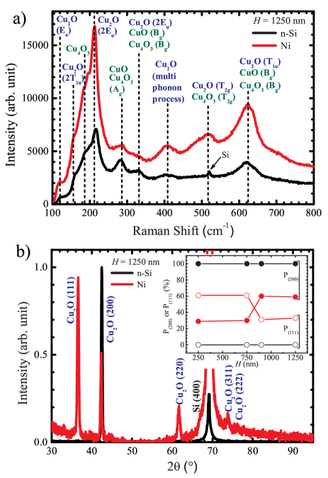
Fig. 1b also shows the XRD patterns of Cu2O films with 1250 nm of thickness deposited on Ni/n-Si(100). The peaks are also in the expected positions for the Cu2O crystal. Cu2O/n-Si(100) samples display strong preferential growth in direction, following the orientation of the substrate. On the other hand, Cu2O film grown on top of Ni/n-Si(100) substrate is composed by grains oriented in , , , and directions.
The evolution of Cu2O growth on Ni/n-Si(100) is explained by Ref. Brandt2014 as follows: (i) the Cu2O films show initial growth due to a better coupling of the Cu2O(111)/Ni(111) interface compared to the Cu2O(100)/Ni(111) one; (ii) at electrolyte pH of the growth is favored, the initial growth starts to be suppressed by the one and at a specific thickness a major part of the Cu2O deposit will be composed by grains.
These growth steps are confirmed by the inset of Fig. 1b, which shows the fraction of the material growing in and directions as a function of film thickness for both substrates. While Cu2O on n-Si(100) is, independently of film thickness, oriented in direction, Cu2O on Ni/n-Si(100) grows up to 750 nm with % of its grains oriented in direction, but only % remain with this orientation in larger thicknesses. The initial growth of Cu2O on Ni(111) is thermodynamically controlled by the Cu2O(111)/Ni(111) coupling, likewise as previously reported for Cu2O(111)/Au(111) and Cu2O(100)/Au(100) interfaces Switzer2002 . However, the crystallographic orientation transition at 750 nm is related to the oxygen concentration in electrolyte at pH , which favors the growth Brandt2014 .
The structure of Cu2O films was checked by cross section TEM images. Figure 2a shows an image obtained from electrodeposited Cu2O film on n-Si(100). A high density columnar microstructure without voids is observed. These columns have a V shape as stressed by discontinuous red lines, exhibiting a grain width increase as a function of film thickness. On the other hand, as seen in Fig. 2b, Cu2O films deposited on the Ni layer under same conditions (solution, temperature and deposition potential) displayed a columnar microstructure with U shape, as indicated in Fig. 2b, and grain width roughly constant as a function of growth time.
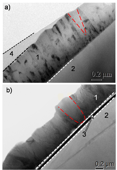
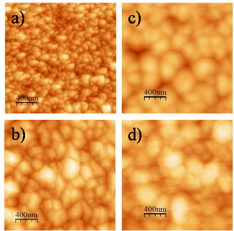
Figure 3 shows AFM images of the films with thicknesses of 250 and 1500 nm. A common feature in both substrates is that the film surface presents a granular aspect. In films deposited on n-Si, there is a remarkable increase of the grain size from the thinnest to the thickest film. The columnar structure with V shape shown in TEM images and this increase in grain size suggest a coarsening process, with part of the initial columns growing and enlarging up to 1500 nm at the expenses of neighboring ones. On the other hand, a mild increase of grain size is observed in the films grown on Ni/n-Si, which is in agreement with TEM images showing columns in U shape.
III.2 Dynamic scaling of surface roughness
The surface roughness is the most used quantity to characterize height fluctuations. For a given surface under a process of kinetic roughening, depends on the lengthscale in which fluctuations are measured. Moreover, given a scanning box with lateral size , the fluctuation in film height inside the box also depends on the box position.
For these reasons, the box roughness is defined as the root-mean-square (rms) fluctuation of the film height () inside a box at a given position, i.e, . The average local roughness of a film of thickness in the lengthscale is the average of the box roughness among all possible box positions. is hereafter simply called roughness.
Using the heights from AFM images, is calculated for Cu2O layers grown on both substrates. The results are shown in Figs. 4a and 4b for a range of thicknesses varying from 25 to 1500 nm. The structural changes induced by substrates n-Si and Ni/n-Si are reflected in topographic differences in the growing surface of the films, confirming the visual inspection of AFM images.
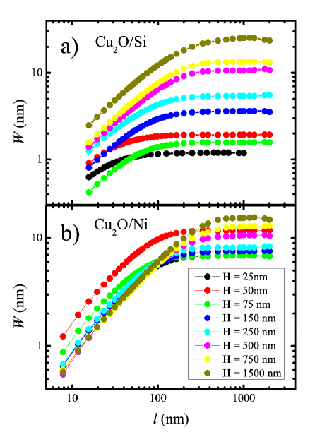
The roughness of films grown on Ni/n-Si show normal dynamic scaling because it is approximately time-independent for small box size and saturates at values increasing with the thickness . Deviations for the thinner samples (25 to 75 nm) are characteristic of the initial island growth and coalescence, indicating that an extended film is formed between 75 nm and 150 nm of thickness. For this reason, only results for nm will be analyzed below.
On the other hand, the oxide layers grown on n-Si have anomalous scaling, since the roughness in small boxes shift to larger values with increasing thicknesses lopez ; ramasco ; huo ; lafouresse . The presence of a single dominant orientation during the growth (shown by XRD) and the coarsening of growing columns from the smallest to the largest thicknesses (suggested by TEM and AFM images) indicate that the scaling anomaly is an intrinsic feature of the surface dynamics in this system.
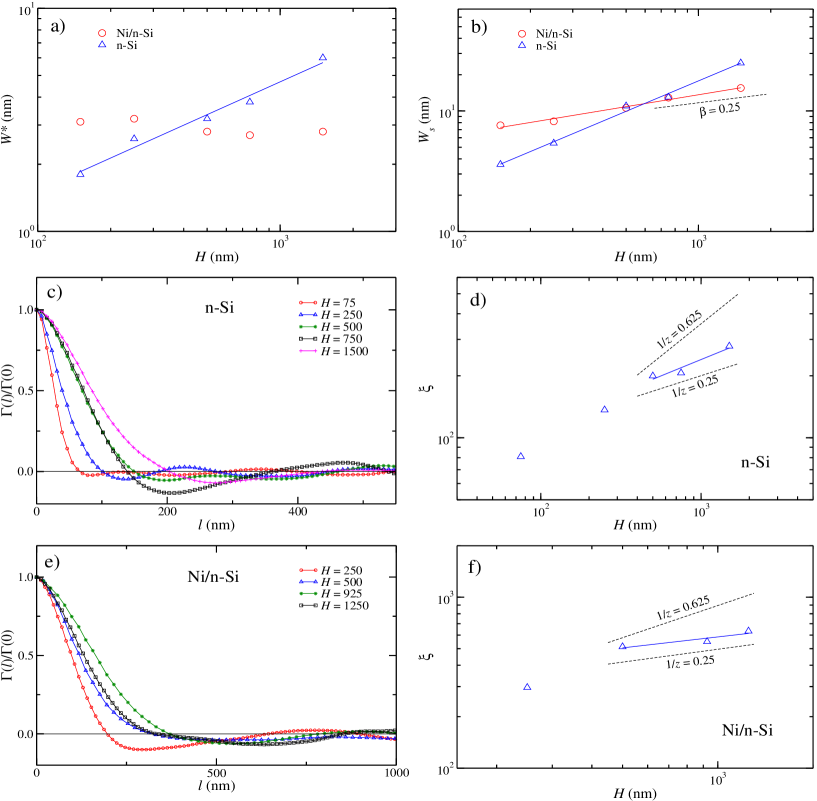
The data presented in Fig. 4 for the thickest films with nm were fit to the relation . It gives estimates of the local roughness exponents and in n-Si and Ni/n-Si substrates, respectively. These values are consistent with the interpretation of granular effects in Refs. tiago2007 and tiago2011 , which predict an exponent near 1 if the maximal box size is smaller than the grain size. Inspection of the AFM images (Fig. 3) supports this hypothesis. These estimates of must not be interpreted as true exponents of dynamic scaling, but as exponents representing the grain shapes tiago2011 .
The local roughness is measured for a fixed small box size nm. It is shown in Fig. 5a as a function of the thickness . For films deposited on Ni, fluctuates around a constant value as the thickness increases, from small values to the largest ones. This is consistent with normal scaling. On the other hand, for films deposited on n-Si, shows a power law increase from small thicknesses ( nm) to the largest ones ( nm). This is the main evidence of anomalous scaling in these films. The fit of the data in Fig. 5a by the scaling relation lopez gives an anomaly exponent ( is also called local slope exponent in theoretical works and local growth exponent in experimental works huo ; lafouresse ).
The saturation values of the roughness in Fig. 4 give the global roughness , which characterize fluctuations of the whole surface at a given thickness. In Fig. 5b, is shown as a function of for both films. The fits to the scaling relation for give the growth exponents and for films deposited on n-Si and Ni/n-Si substrates, respectively.
Since the growth on Ni/n-Si substrates has normal scaling, we search for a model of local stochastic growth equation, which may disclose the main mechanisms of the surface dynamics barabasi ; krug . The above estimate of is larger than the values provided by the equations of second and fourth orders, which are in the range barabasi . However, Fig. 5b shows that a slope close to cannot be discarded for large thicknesses. This is close to the exponents of the Kardar-Parisi-Zhang (KPZ) class kpz , fabio2004 ; kelling , and of the Mullins-Herring (MH) class mh , .
Information on surface correlations can be obtained from the spatial correlation function at time , with . The rescaled functions of the oxide films respectively grown on n-Si and Ni/n-Si substrates are shown in Figs. 5c and 5e as a function of the distance , for several thicknesses. A reliable estimate of the correlation length is the minima of Almeida2014 ; siniscalco , which is shown in Figs. 5d and 5f as a function of the thickness .
The estimates of are close to those obtained by intersection of straight line fits of the roughness in the growth and saturation regimes, which is a usual method in the analysis of experimental data. Ref. zoldan2005 shows that this method leads to estimates of of the same order of the average grain size estimated by inspection of microscopy images zoldan2005 . However, an accurate calculation of the average grain size is more complicated siniscalco and not performed here.
The scaling is expected for large thicknesses barabasi ; krug . Linear fits of the data for nm give estimates and (dynamic exponents and ) for growth on n-Si and Ni/n-Si substrates, respectively. These exponents are very different from the KPZ value fabio2004 ; colaiori . On the other hand, the Figs. 5d and 5f show that the slopes of the plots for the largest thicknesses are close to the MH value (the corresponding slope of KPZ scaling is also shown for comparison).
The MH equation is a model for growth dominated by surface diffusion of adsorbed species mh :
| (1) |
where is the interface height at substrate position and time , is a constant, and is a Gaussian (nonconservative) noise with covariance amplitude barabasi ; mh . A constant external flux was omitted from Eq. (1), which corresponds to a spatially uniform and time-independent adsorption rate. Thus, the local growth rate of the MH model is not affected by diffusion in solution, for instance due to the presence of diffusive layers, shadowing effects etc.
On the other hand, the KPZ equation is a model for interface growth dominated by surface tension and by a nonlinear effect of the local slope kpz :
| (2) |
where and are constants. Distinguishing these possibilities is an important step to understand the microscopic growth dynamics of the oxide films. The KPZ model also assumes spatially uniform and time-independent adsorption rate, with no effect of diffusion in solution to the local growth rate.
III.3 Scaling of distributions
We now turn to the analysis of distributions of heights and of local quantities, which was recently shown to be a more powerful tool to the study of kinetic roughening of thin films Almeida2014 ; healy2014 ; Almeida2015 .
The height distribution is defined as the probability density of the height , so that gives the probability of finding a height in the range . Figures 6a and 6c, and 6b and 6d show the scaled height distributions of the oxide films with large thicknesses, respectively grown on n-Si and Ni/n-Si substrates. They are compared with distributions of the KPZ and MH classes in the growth regimes. The KPZ distribution was numerically calculated in Refs. halpin2012 and tiagorapid2013 . For the MH class, the distribution is Gaussian, which was confirmed by direct integration of the MH equation [Eq. 1] and by simulation of the large curvature model (LCM) lcm .
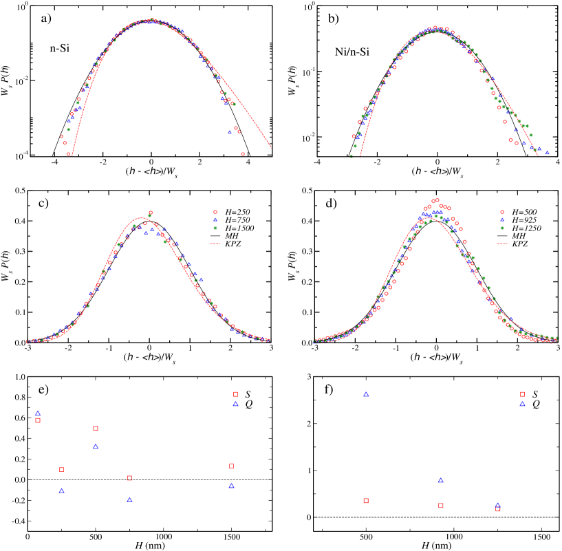
The experimental data in Figs. 6a, 6b, 6c and 6d are closer to the Gaussian/MH curve. The symmetric shape clearly contrasts with the asymmetry of the KPZ curve. Indeed, the skewness and kurtosis of the distributions, shown in Figs. 6e and 6f, drops to zero as the thickness increases (consistently with Gaussian/MH), while the asymptotic KPZ values are and halpin2012 ; tiagorapid2013 .
Another important conclusion emerges from Figs. 6a and 6b: since the scaled height distributions are the same for films deposited on n-Si and on Ni/n-Si, the main physico-chemical processes responsible for their roughening are the same.
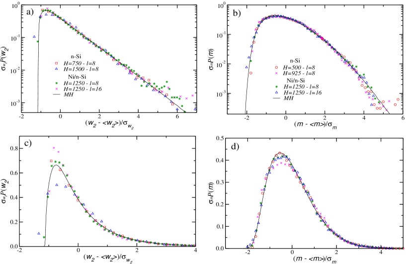
The distribution of the squared box roughness is defined so that is the probability that the squared roughness in a given box is in the range racz1994 ; antal2002 . Figures 7a and 7c compares the scaled roughness distributions of the oxide films grown on both substrates and that of the MH class in the growth regime ( is the rms fluctuation of ). The size of the box in which is measured ranges from 100 nm to 300 nm. The MH curve is calculated by integration of the MH equation in the growth regime.
In Figs. 7a and 7c, the collapse of the scaled distributions for films grown in different substrates is clear, which is additional support to the proposal that their roughening is governed by the same physico-chemical processes (despite the very different structures of those films). Good agreement with the MH curve reinforces the proposal that diffusion of adsorbed species is the main mechanism of the surface dynamics.
We also analyzed the distribution of the maximal relative height in the growth regime. Here, and are, respectively, the maximal and the average heights measured inside each box position. The distributions for both films are shown in Figs. 7b and 7d, showing good data collapse among them and with the MH curve.
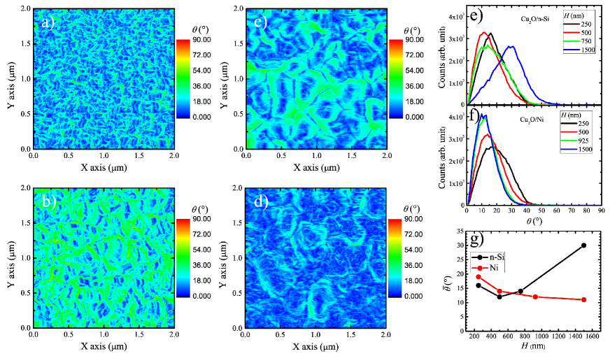
Following the procedure described in Ref. walther , we also calculated the local surface slope using the AFM images. The local slope images corresponding to the height images shown in Fig. 3 are displayed in Fig. 8. They clearly show that larger values for are obtained in intergranular regions, while small are related to flat areas near the top of Cu2O grains.
The distributions of local slopes are shown in Figs. 8e and 8f for Cu2O/n-Si and Cu2O/Ni films, respectively. The position of the peaks of those distributions are displayed in Fig. 8g as a function of thickness. For films grown on n-Si, the distribution significantly changes as the thickness increases, with an increase in . This is typical of anomalous scaling lopez ; ramasco and is qualitatively consistent with the local roughness increase shown in Fig. 5a. On the other hand, for films grown on Ni/n-Si, average local slopes decrease with the thickness, saturating in the thicker films. This is consistent with normal scaling. Comparison of local slope distributions with those of theoretical models is not possible because there are significant thickness effects and the present concept of local slope differs from the definitions in integrated growth equations or in lattice models.
The MH scaling was formerly observed in electrochemically deposited Prussian Blue films alamini . In that case, the anomalous roughening was generated by time increasing adsorption rates.
III.4 Extended analysis of MH scaling
The exact solution of the MH equation krug ; amar1993 allows an extension of the interpretation of the experimental data, particularly those of films grown on n-Si substrates.
The MH roughness is expected to scale similarly to the height-height correlation function; in terms of box size and time we have krug
| (3) |
where is a scaling function [ for small ] and
| (4) |
Recall that is proportional to the time .
The long time (large thickness) scaling of the correlation length gives exponent near the MH value (). Thus, Eq. 4 indicates that is approximately time-independent. The coefficient in Eq. 1 represents the relation between surface diffusion coefficients and local surface geometry of a given material. This relation is not expected to change in the course of the (constant temperature) deposition.
For , Eq. 3 suggests that the local roughness (measured for fixed nm; Sec. III.2) scales as . Figure 9 shows versus for both films. The approximately constant value of for the films grown on Ni/n-Si indicates that is also time-independent in that case. However, the scaling in films grown on n-Si and the time-independence of gives . Since is the amplitude of time and spatial fluctuations of deposition rate, this means that those fluctuations increase in time in the films grown on n-Si. This leads to the anomalous scaling in those films.
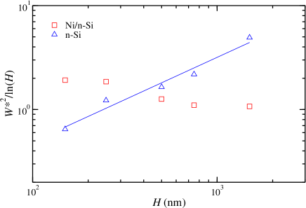
The above increase of is sufficiently slow, thus the original solution of the MH equation can be consistently used with the time-dependent form of that parameter krug ; amar1993 . This feature was already illustrated in other continuous and lattice models with time dependent couplings anomalouscompetitive ; pradas2006 showing anomalous scaling.
IV Discussion and conclusion
The scaling of distributions of local heights, maximal heights, and roughness provide strong evidence that the roughening in electrodeposited Cu2O films is governed by the MH equation (1). The noise amplitude increases in time in the equation associated to the films grown on n-Si substrates, corresponding to the scaling anomaly. This analysis clearly advance over the calculation of scaling exponents, which however are also compatible with the MH ones.
The MH equation was proposed for roughening in molecular beam epitaxy barabasi , in which a crystalline film slowly grows by random adsorption of atoms/molecules from vapor and surface adatoms diffuse and preferentially bind to high coordination (low energy) sites. Thus, in the electrochemical deposition of Cu2O films, those results indicate that this interplay of surface diffusion and deposition noise is also the main ingredient for roughening under the present growth conditions.
The MH equation considers that adsorption rates are spatially uniform and do not depend on time. This suggests that electrochemical conditions do not determine the main dynamic mechanisms for roughening, although they probably affect the values of the parameters in the associated MH equation. Since the same electrochemical conditions were used for growth of films on both substrates, we are led to the conclusion that their different structures are consequence of the substrate-film interaction. The different interactions in different substrates determine the island nucleation and growth and has consequences in the thickest films, despite the universal MH dynamics
The connections between the microscopic dynamics and the structure of the growing films can be derived from our results, as follows.
In systems with diffusion-dominated dynamics, molecules at a surface grain randomly move, with rates depending on local energy barriers. At first approximation, those barriers depend on coordination numbers and increase at step edges. For an adatom or ad-molecule to go down a step, the additional activation energy, known as Ehrlich-Schwoebel (ES) barrier ehrlich ; schwoebel , reduces the downward flux near the step edge, favoring nucleation of new atomic terraces over the ones previously formed evansreview . The effect of ES barriers is enhanced at grain boundaries, constraining the mass flux between the grains if height differences are large. These features are observed in films of several materials grown by vapor methods. The above results strongly suggest to extend this interpretation to Cu2O electrodeposition.
Figure 3a shows that films grown on n-Si substrates have an initially small average grain size, but with a broad size distribution. This is confirmed quantitatively by the small values of the correlation length in Fig. 5d ( nm in nm thick films). Thus, the islands nucleating at that substrate also had large size fluctuations. This may be a consequence of large spatial fluctuations of the adsorption rate during the first stages of the growth.
When an extended film is formed, the local adsorption rates may become uniform, particularly if the dominant crystallographic orientation does not change, as shown in Sec. III.1; see also inset of Fig. 1b. However, larger grains have larger numbers of terraces and steps, consequently the mass flux from their tops to their boundaries is small. With restricted mass exchange in grain boundaries, the large grains increase in width and cover the smaller ones. From a coarse grained point of view, the fluctuations in the adsorption rate continue to increase, which qualitatively explains the time increase of the parameter in the corresponding hydrodynamic model (the MH equation).
Figure 8e shows that the shape of the slope distribution is the same while its average value moves to the right during the film growth. This means that local slopes increase inside the grains and at their boundaries, consistently with the above interpretation.
On the other hand, Fig. 3c shows that films grown on Ni/n-Si substrates have larger initial grains with a much narrower size distribution (see also insets of Figs. 5d and 5f). This is related to small fluctuations in local adsorption rates, a feature that is maintained during the growth and leads to normal roughening.
AFM images also reveal that the grain top surfaces are similar in the films grown in both substrates, thus the local (microscopic) adsorption rates at those surfaces are expected to be the same. In growth on n-Si substrates, the difference in the net growth rate of individual grains have to be explained by the restricted mass flux across grain boundaries, not by intra-grain features. If some grains with large slopes are initially formed, they may grow faster at the expenses of the neighboring ones. This establishes a connection between the V-shaped grains and the anomalous roughening.
Unusual scaling features are frequently found in diffusion-dominated growth in the presence of step energy barriers evansreview . For instance, a small barrier in Fe/Fe(100) epitaxy leads to mound formation at the film surface, with skewed height distribution and barteltPRL1995 , which are characteristics of the non-linear molecular beam epitaxy equation villain ; laidassarma . Moreover, mound steepening in Ag/Ag(100) epitaxy at room temperature occurs with an effective exponent much larger than in thicknesses ranging from 100 to 1000 monolayers caspersenPRB2002 ( is a feature of completely uncorrelated growth barabasi ).
We conclude that, although control of electrochemical conditions is essential to enable growth of Cu2O films and to determine the crystallographic orientation, our results show that large scale surface features are determined by physical properties of the material and the substrate, with consequences on the internal film structure. Roughening is governed by the interplay of deposition and ad-species surface diffusion, similarly to vapor deposition, with no significant influence of inhomogeneous mass flux from the solution (if it exists). However, substrate-film interactions have a strong effect on island nucleation and growth, thus the structure of the tickest films is drastically affected by these initial conditions, despite the universal (MH) roughening dynamics.
Acknowledgements.
The authors acknowledge financial support from CAPES, CNPq (NAMITEC and Nanoinstrumenta o), FAPESC, FAPEMIG and FAPERJ (Brazilian agencies). LCME, LabMat and LDRX laboratories of the Universidade Federal de Santa Catarina for the use of the TEM, Raman spectroscopy and XRD facilities.References
- (1) R. G. Delatorre, M. L. Munford, R. Zandonay, V. C. Zoldan, A. A. Pasa, W. Schwarzacher, M. S. Meruvia, and I. A. Hümmelgen, Appl. Phys. Lett. 88, 233504 (2006).
- (2) D. P. Joseph, T. P. David, S. P. Raja, and C. Venkateswaran, Mater. Charact. 59, 1137 (2008).
- (3) C. G. Morales-Guio, S. D. Tilley, H. Vrubel, M. Grätzel, and X. Hu, Nat. Commun. 5, 3059 (2014).
- (4) M.-J. Deng, C.-Z. Song, P.-J. Ho, C.-C. Wang, J.-M. Chen, and K.-T. Lu, Phys. Chem. Chem. Phys. 15, 7479 (2013).
- (5) X.-W. Liu, Langmuir 27, 9100 (2011).
- (6) F. Oba, F. Ernst, Y. Yu, R. Liu, H. M. Kothari, and J. A. Switzer, J. Am. Ceram. Soc. 88, 253 (2005).
- (7) A. Chen, H. Long, X. Li, Y. Li, G. Yang, and P. Lu, Vacuum 83, 927 (2009).
- (8) J. Deuermeier, J. Gassmann, J. Brötz, and A. Klein, J. Appl. Phys. 109, 113704 (2011).
- (9) A. Mittiga, E. Salza, F. Sarto, M. Tucci, and R. Vasanthi, Appl. Phys. Lett. 88, 163502 (2006).
- (10) Z. Zang, A. Nakamura, and J. Temmyo, Opt. Express 21, 11448 (2013).
- (11) T. D. Golden, M. G. Shumsky, Y. Zhou, R. A. VanderWerf, R. A. Van Leeuwen, and J. A. Switzer, Chem. Mater. 8, 2499 (1996).
- (12) J. A. Switzer, H. M. Kothari, and E. W. Bohannan, J. Phys. Chem. B 106, 4027 (2002).
- (13) I. S. Brandt, C. A. Martins, V. C. Zoldan, A. D. C. Viegas, J. H. D. da Silva, and A. A. Pasa, Thin Solid Films 562, 144 (2014).
- (14) S. Bijani, L. Martínez, M. Gabás, E. A. Dalchiele, and J.R. Ramos-Barrado, J. Phys. Chem. C 113, 19482 (2009).
- (15) K. Han, and M. Tao, Sol. Energy Mater. Sol. Cells 93, 153 (2009).
- (16) Y. D. Gamburg, and G. Zangari, Theory and Practice of Metal Electrodeposition (Springer, 2011), p. 378.
- (17) A. Paracchino, J. C. Brauer, J.-E. Moser, E. Thimsen, and M. Graetzel, J. Phys. Chem. C 116, 7341 (2012).
- (18) R. C. da Silva, A. A. Pasa, J. J. Mallett, W. Schwarzacher, Surf. Sci. 576, 212 (2005).
- (19) A.-L. Barabasi and H. E. Stanley, Fractal Concepts in Surface Growth (Cambridge University Press, Cambridge, England, 1995).
- (20) J. Krug, Adv. Phys. 46, 139 (1997).
- (21) J. W. Evans, P. A. Thiel, and M. C. Bartelt, Surf. Sci. Rep. 61, 1 (2006).
- (22) Q. Hua, D. Shang, W. Zhang, K. Chen, S. Chang, Y. Ma, Z. Jiang, J. Yang, and W. Huang, Langmuir 27, 665 (2011).
- (23) S. Somasundaram, C. R. N. Chenthamarakshan, N. R. de Tacconi, and K. Rajeshwar, Int. J. Hydrogen Energy 32, 4661 (2007).
- (24) I. Pallecchi, L. Pellegrino, N. Banerjee, M. Cantoni, A. Gadaleta, A. S. Siri, and D. Marré, Phys. Rev. B 81, 165311 (2010).
- (25) R. G. Delatorre, V. Stenger, V. C. Zoldan, D. L. da Silva, S. G. dos Santos, A. D. C. Viegas, and A. A. Pasa, ECS Trans. 23, 77 (2009).
- (26) B. K. Meyer, A. Polity, D. Reppin, M. Becker, P. Hering, P. J. Klar, T. Sander, C. Reindl, J. Benz, M. Eickhoff, et al., Phys. Status Solidi 249, 1487 (2012).
- (27) J. M. López, Phys. Rev. Lett. 83, 4594 (1999).
- (28) J. J. Ramasco, J. M. López, and M. A. Rodríguez, Phys. Rev. Lett. 84, 2199 (2000).
- (29) S. Huo, and W. Schwarzacher, Phys. Rev. Lett. 86, 256 (2001).
- (30) M. C. Lafouresse, P. J. Heard, and W. Schwarzacher, Phys. Rev. Lett. 98, 236101 (2007).
- (31) T. J. Oliveira and F. D. A. A. Reis, J. Appl. Phys. 101, 063507 (2007).
- (32) T. J. Oliveira and F. D. A. Aarao Reis, Phys. Rev. E 83, 041608 (2011).
- (33) M. Kardar, G. Parisi, and Y.-C. Zhang, Phys. Rev. Lett. 56, 889 (1986).
- (34) F. D. A. Aarao Reis, Phys. Rev. E 69, 021610 (2004).
- (35) J. Kelling and G. Ódor, Phys. Rev. E 84, 061150 (2011).
- (36) W. W. Mullins, J. Appl. Phys. 28, 333 (1957); C. Herring, in The Physics of Powder Metallurgy, edited by W. E. Kingston (McGraw-Hill, New York, 1951).
- (37) R. A. L. Almeida, S. O. Ferreira, T. J. Oliveira, and F. D. A. Aarao Reis, Phys. Rev. B 89, 045309 (2014).
- (38) D. Siniscalco, M. Edely, J.-F. Bardeau, and N. Delorme, Langmuir 29, 717 (2013).
- (39) V. C. Zoldan, D. M. Kirkwood, G. Zangari, M. L. Munford, W. Figueiredo, and A. A. Pasa, Microsc. Microanal. 11, 154 (2005).
- (40) F. Colaiori and M.A. Moore, Phys. Rev. Lett. 86, 3946 (2001).
- (41) T. Halpin-Healy and G. Palasantzas, Europhys. Lett. 105, 50001 (2014).
- (42) R. A. L. Almeida, S. O. Ferreira, I. R. B. Ribeiro, and T. J. Oliveira, Europhys. Lett. 109, 46003 (2015).
- (43) T. Halpin-Healy, Phys. Rev. Lett. 109, 170602 (2012); Phys. Rev. E 88, 042118 (2013).
- (44) T. J. Oliveira, S. G. Alves and S. C. Ferreira, Phys. Rev. E 87, 040102(R) (2013).
- (45) J. M. Kim and S. Das Sarma, Phys. Rev. Lett. 72, 2903 (1994).
- (46) G. Foltin, K. Oerding, Z. Rácz, R. L. Workman, and R. K. P. Zia, Phys. Rev. E 50, R639 (1994).
- (47) T. Antal, M. Droz, G. Györgyi, and Z. Rácz, Phys. Rev. E 65, 046140 (2002).
- (48) L. Liu and W. Schwarzacher, Electrochem. Commun. 29, 52 (2013).
- (49) M. F. Alamini, R. C. da Silva, V. C. Zoldan, E. A. Isoppo, U. P. R. Filho, F. D. A. A. Reis, A. N. Klein, and A. A. Pasa, Electrochem. Commun. 13, 1455 (2011).
- (50) J. G. Amar, P.-M. Lam, and F. Family, Phys. Rev. E 47, 3242 (1993).
- (51) F. D. A. Aarão Reis, Phys. Rev. E 84, 031604 (2011).
- (52) M. Pradas and A. Hernández-Machado, Phys. Rev. E 74, 041608 (2006).
- (53) R. L. Schwoebel and E. J. Shipsey, J. Appl. Phys. 37, 3682 (1966).
- (54) G. Ehrlich and F. G. Hudda, J.Chem. Phys. 44, 1039 (1966).
- (55) M. C. Bartelt and J. W. Evans, Phys. Rev. Lett. 75, 4250 (1995).
- (56) J. Villain, J. Phys. I 1, 19 (1991).
- (57) Z.-W. Lai and S. Das Sarma, Phys. Rev. Lett. 66, 2348 (1991).
- (58) K. J. Caspersen, A. R. Layson, C. R. Stoldt, V. Fournee, P. A. Thiel, and J. W. Evans, Phys. Rev. B 65, 193407 (2002).