Half-metallic Dirac cone in zigzag-graphene-nanoribbon/graphene
Abstract
The Dirac electrons of graphene, an intrinsic zero gap semiconductor, uniquely carry spin and pseudospin that give rise to many fascinating electronic and transport properties. While isolated zigzag graphene nanoribbons are antiferromagnetic semiconductors, we show by means of first-principles and tight-binding calculations that zigzag graphene nanoribbons supported on graphene are half-metallic as a result of spin- and pseudospin-symmetry breaking. In particular, half-metallic Dirac cones are formed at K (K’) near the Fermi level. The present results demonstrate that the unique combination of spin and pseudospin in zigzag graphene nanoribbons may be used to manipulate the electronic properties of graphene, and may have practical implications for potential graphene-based nanoelectronic applications.
pacs:
71.20.-b,73.20.-r,73.22.Pr,75.75.-cI Introduction
The discovery of graphene has inspired intense interest in graphene-based nanostructures and their derivatives such as van der Waals (vdW) heterostructures.Novoselov et al. (2005); Geim and Grigorieva (2013) One fascinating feature of graphene is the combination of real spin and pseudospin which gives rise to rich physics in this unique two dimension system, e.g., unusual quantum Hall effect.Zhang et al. (2005) Breaking these symmetries could lead to interesting physical phenomena, Sodemann and MacDonald (2014); Zhou et al. (2007); Young et al. (2012); Yao et al. (2008) such as gap opening due to pseudospin symmetry breaking in supported graphene,Zhou et al. (2007) additional Hall plateau induced by SU(4) spin-pseudospin symmetry breaking due to electron-electron interaction,Young et al. (2012) and valley polarization caused by inversion symmetry breaking.Yao et al. (2008)
Graphene can be patterned into a variety of one dimensional nanoribbons, of which electronic properties are strongly dependent on the ribbon width and edge patterns. Han et al. (2007); Hod et al. (2007); Wassmann et al. (2008); Lee and Cho (2009); Li et al. (2008, 2013a) Among them, zigzag graphene nanoribbons (ZGNRs) have attracted particular attention owing to their unique edge magnetism, Son et al. (2006); Huang et al. (2007, 2008); Lee and Cho (2009); Li et al. (2008); Pan et al. (2011); Li et al. (2013a); Jung et al. (2009); Magda et al. (2014) which can be strongly suppressed by metal substrates. Chen et al. (2012); Li et al. (2013b, c); Zhang et al. (2013) Recently, H-terminated ZGNRs on graphene substrate were obtained by cutting the top layer of graphene bilayer using hydrogen etching method.Li et al. (2014) Because of the van der Waals interaction between the GNRs and the substrate, this type of system provides an ideal platform for studying electronic properties of GNRs. For instance, edge states were explicitly observed in STM/STS experiments and a critical width of about 3 nm was revealed for the onset of electron-electron correlation between the edges of anti-ferromagnetic (AFM) ZGNRs.Li et al. (2014)
The edge states of ZGNRs also carry unique spin and pseudospin information: spins are ferromagnetically coupled along each edge but antiferromagnetically coupled between edges, i.e., along each edge the spin polarized state is spatially located on only one sublattice (pseudospin). Here we demonstrate, based on density functional theory (DFT) and tight binding (TB) calculations, that the unique combination of spin and pseudospin in ZGNRs can also be used to manipulate properties of graphene. A half-metallic state is surprisingly obtained in AB (Bernal) stacking of ZGNR on graphene as a result of spin- and pseudospin-symmetry breaking caused by the interaction between the GNR and graphene substrate. Remarkably, half-metallic Dirac cones are formed at K (K’) near the Fermi level.
II COMPUTATIONAL DETAILS
To study the electronic and magnetic properties of AFM ZGNRs supported by graphene, we carried out spin-polarized first-principles electronic-structure calculations using the Vienna Ab initio Simulation Package. Kresse and Furthmüller (1996a, b) The exchange-correlation functional was parametrized in terms of the local density approximation according to Ceperley and Alder,Ceperley and Alder (1980) and pseudopotentials were constructed by the projector augmented wave method.Blöchl (1994); Kresse and Joubert (1999) The one-dimensional Brillouin zone was sampled by a 1241 Monkhorst-Pack mesh for the self-consistent calculations.
III Results
III.1 DFT calculations
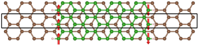
Figure 1 schematically illustrates the structure of H-terminated AFM-ZGNR/graphene with AB stacking. The ribbon is separated from its periodic images by 12 Åvacuum regions. In both the DFT and the TB calculations the spin up (down) density corresponds to the majority spin of the left (right) edge of the nanoribbon, which is over the top (hollow) sites of the graphene substrate. Our DFT calculations indicate that edge magnetism of AFM-ZGNRs is preserved in the presence of graphene, with a magnetic moment 0.13 per edge atom for both the freestanding and supported ZGNRs. Although the magnitudes for the two edge are slightly different for the supported system, the difference is small; for example, for 32-ZGNR/graphene, the two edges have moments of 0.128 and 0.136 , respectively. (The magnetic moments on the edge atoms obtained in the present study are much smaller than the one (0.43 ) reported by Ref. Son et al., 2006, but consistent with Ref. Huang et al., 2008. However, we note that larger moments (0.4 ) can be obtained if the core correction to the density is neglected.)
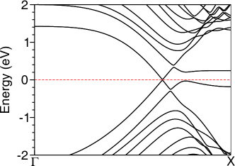
To see the effects of stacking on the electronic structure of ZGNRs on graphene, calculations were also performed for AA stacking 8-ZGNR/graphene. As shown in Fig. 2, AA stacking induces a small gap of about 0.03 eV at the K point. The two spins are degenerate since AA stacking maintains the inversion symmetry of the nanoribbon.
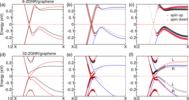
Figures 3a and d display the electronic bands for 8- and 32-ZGNR/graphene, respectively. Compared to AA stacking, a spin splitting is obtained for AB stacking ZGNR/graphene. The gap opening that occurs at the projection of the K point () of graphene is spin-dependent: it is much larger for spin-up – the majority spin of the left edge (on top sites) – than that for spin down, the majority spin of the right edge (in hollow sites). In particular, for spin down the gap between the valence band and the conduction band is negligibly small at K. The trend in the gap opening is in fact associated with the location of the edge atom (top sites versus hollow sites). The Fermi level crosses bands of only one spin state, making the whole system half-metallic as a result of the nanoribbon-graphene interaction that induces small magnetization in the graphene and a net magnetic moment to the whole system.
Figures 3b, c show the electronic bands for 8-ZGNR/graphene weighted by the localization on the graphene substrate and the nanoribbon, respectively; Figs. 3e and f are the corresponding plots for 32-ZGNR/graphene. One can see that the bands for 8-ZGNR/graphene at K near the Fermi level are basically graphene bands. For 32-ZGNR/graphene, both constituents have considerable contributions, as expected since the bands evolve toward the properties of graphene bilayer as the ribbon size increases. Band analysis further reveals that the four bands (including spin) at K are contributed by the hollow sites only, consistent with the limit of graphene bilayer. However, instead of the four-fold degeneracy at the K point in a graphene bilayer, for AFM-ZGNRs/graphene the four bands split as a result of spin and pseudospin symmetry breaking. From Figs. 3c and f one can see a shift in the edge states near the X point, that is, the bands for the left edge (top sites) are shifted upward relative to those for the right edge (hollow sites). The underlying physics is that the AB stacking of AFM-ZGNRs and graphene gives rise to different electrostatic potentials for different edges: Because the edge states are mainly localized to one sublattice, especially near the X point, they are either at the top or hollow sites. The AB stacking raises the electrostatic potential of the top sites more than the hollow sites, resulting in a relative shift in the bands for the two edges. This mechanism is similar to the case of freestanding AFM ZGNRs under external electric field.Son et al. (2006) Dramatic changes can be seen as the point approaches K, where the shift of the conduction bands of the two spins is opposite to the case near the X point. This behavior is related to the interaction between states of AFM ZGNRs and graphene involving special spin- and pseudospin-symmetry breaking (see discussions below).
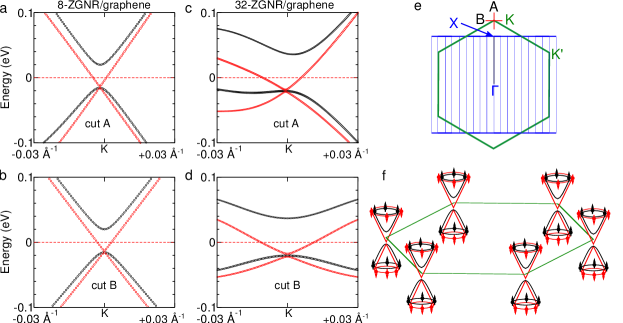
To further explore the properties of the bands at K (K’), Fig. 4 depicts the -projected bands around K for both 8-ZGNR/graphene and 32-ZGNR/graphene, obtained by projecting the wave functions of AFM-ZGNR/graphene in the rectangular supercell onto the 11 cell of grapheneQi et al. (2010); Chen and Weinert (2014) (c.f., Fig. 4e). Half-metallic Dirac states about K exist for all the studied systems. However, unlike for ideal graphene, the Dirac cone for ZGNRs/graphene is anisotropic, i.e., the linear dispersions along -K and its perpendicular direction are different, leading to anisotropic Fermi velocities in ZGNRs/graphene due to the one-dimensional nature of the nanoribbon. Moreover, the linear dispersions for 32-ZGNR/graphene experience a significant renormalization, as expected since the bands about K approach those of a graphene bilayer. (Calculations were also performed about K’, which give rise to the same band structures as required by symmetry and are not shown here.) Fig. 4f schematically show the half-metallic Dirac cones at K and K’ in the Brillouin zone (BZ) of graphene.
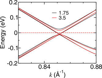
A question arises whether the half-metallic behavior seen near K is an artifact of the choice of supercell, in particular the ratio of the graphene substrate to the nanoribbon. Although a calculation for an AFM-ZGNR on infinite graphene is obviously infeasible, we performed a calculation for 8-AFM-ZGNR on graphene by doubling the ratio, i.e., the ratio of the area of the graphene to that of the nanoribbon is increased to 3.5 from 1.75. Such a structure gives rise to 45 Åseparations between the nanoribbon and its periodic images on the graphene substrate. Figure 5 shows that there are only minor changes in the band structure near K when the ratio is doubled; in particular, the half-metallic behavior is well preserved. The gap for spin down, however, is slightly reduced, as the substrate bands approach those of a single graphene layer in the limit of infinite graphene. Nevertheless, one may still expect half-metallic behavior as long as there exists the spin- and pseudospin symmetry breaking which are caused by the presence of the AFM ZGNR and the AB stacking.
Another possible issue is the effect of vdW dispersion forces between the nanoribbon and the substrate. To investigate such effects vdW-DF calculations were performed for 8-AFM-ZGNR/graphene using the method developed by Klimeš and Michaelides,Klimeš et al. (2011, 2010) for which the optB88-vdW functional was used for the exchange functional. The equilibrium layer distance derived from these calculation is about 3.46 Å, close to the 3.35 Åused for the above calculations, and thus the calculated band structure (not shown), is very similar to that shown in Fig. 3a, including half-metallic nature.
III.2 Tight-binding calculations
The half-metallic states near K originate from the spin and pseudospin-symmetry breaking due to the special stacking of the two constituents, which can be understood by a tight-binding model. The Hamiltonian for the graphene can be written as
| (1) |
The edge states of ZGNRs can be described by the Hubbard model within the Hartree-Fock approximation Wakabayashi et al. (2010); Hancock (2010)
| (2) |
where and are creation and annihilation operators for spin at site , respectively, , and and denote hopping integrals and on-site Coulomb interaction between electrons, respectively. The respective chemical potentials are . The self-consistent solution to Eq. (2) gives rise to
| (3) |
with respect to the symmetry center, where and are the two sublattices corresponding to the different edges. Note that Eq. (3) implies spin degeneracy in freestanding AFM ZGNRs. In our calculations was set to 2.0 eV and the include up to the second-nearest-neighbor interaction according to Ref [Hancock, 2010], such that electronic bands derived from TB calculations are in good agreement with ab initio results for the free standing nanoribbons.
The Hamiltonian describing the interaction between the ZGNR and graphene has the form
| (4) |
where and are creation and annihilation operators for the two constituents, respectively. describes the hopping between atom in the nanoribbon and atom in graphene. In AB stacking, top-site carbon atoms experience stronger perturbation than those in hollow sites. This physics can be captured by considering hopping only between the nearest top-top sites, properly chosen so that TB calculations reproduce the bands of graphene bilayer about the K point. As a consequence of breaking the spin symmetry in Eq.(3), the two edge states of the nanoribbon, which carry different spins, are no long degenerate. Similarly, the interaction breaks the spin and pseudospin-symmetry in graphene in the same manner.
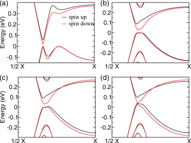
Figures 6a, b display the electronic bands derived from the TB calculations for 8-ZGNR/graphene and 32-ZGNR/graphene, respectively. These calculations show the same trend as DFT calculations: the gap opening for the the majority spin of the top sites is much larger than the one for the other spin. If the on-site energies for the top and hollow sites are treated differently, as commonly done for graphene bilayers, a band shifting at the Brillouin zone (BZ) boundaries (the X point) is obtained (Fig. 6c). Because of magnetic proximity effect, the coupling of an AFM ZGNR to graphene leads to spin polarization in graphene. In this sense, introducing weak magnetism in graphene shrinks the gap opening (Fig. 6d). In particular, the gap for spin down becomes extremely small, consistent with the DFT calculations.
III.3 Low energy model calculations
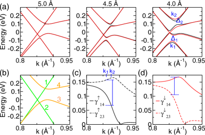
To see how the nanoribbon-graphene interaction affects the gap openings at K, we vary the layer distance gradually from 5 to 4 Å. Because the half-metallic feature is more pronounced for larger ZGRNs, calculations were carried out for 32-ZGNR/graphene only, with the results are summarized in Fig. 7a. The gap openings at K are accompanied by two band splittings at (for the valence band) and (for the conduction band) labeled as and , respectively, resulting from the interaction between the nanoribbon bands 3 and 4 of Fig. 7b and the linear dispersing bands of the graphene substrate. Based on the bands of the isolated systems shown in Fig. 7b, the band splittings is due to the interaction between bands 2 and 3, whereas is attributed to the interaction between bands 1 and 4. For spin up, which has a sizable gap at K, is much larger than . For spin down, however, grows and becomes larger than as the interlayer separation decreases. Such an enhanced splitting pushes the bonding state (resulting from the interaction between bands 1 and 4) down further, reducing the gap with the antibonding state resulting from the interaction of bands 2 and 3.
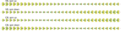
The behavior of and is inherently related to the characteristics of the wave functions of the edge states in AFM ZGNR. Unlike in graphene where the two sublattices make equal contributions to the linear dispersing bands, they make asymmetric contributions to the valence and conduction bands of AFM ZGNRs. At the zone boundary (X point), the valence and conduction band edge states are completely localized on only one sublattice, either top sites or hollow sites. As the point varies along X–K, these states involve an increasing contribution of the other sublattice but a large asymmetry in the contributions of the two sublattices remains. For instance, Fig. 8 shows that the valence band for freestanding 32-ZGNR near the K point is mainly contributed by top sites for spin up and by hollow sites for spin down, and for the conduction band the situation is opposite. Therefore, one may expect a larger for spin up than spin down, as well as a larger for spin down when the coupling to graphene in the AB stacking shown in Fig. 1.
To gain further insights into the interaction, a 44 low energy Hamiltonian for the four bands is constructed.
| (9) |
where describe the interaction between the bands of graphene and those of AFM-ZGNRs shown in Fig. 6b. The matrix elements are calculated based on the eigenvectors of the freestanding systems:
| (10) |
where and are derived from Eq. (1) and Eq. (2), respectively, and stand for the coupling strength and phase factor, respectively.
The band splittings and are mainly the consequence of and , respectively. Figures 7c and d show the magnitudes of and for the two spins, respectively, i.e., and . Opposite trends are observed for the two couplings by a comparison of the two plots: is larger than , but has a smaller value than . Thus, one may have a larger for spin up than spin down, as well as a larger for spin down than spin up. Fig. 7c shows that is larger than , while Fig. 7d indicates an opposite trend. Moreover, for spin up the difference between and is much larger than that for spin down, leading to a noticeable difference between and for spin up, consistent with the observation in Fig. 7(a). The 44 Hamiltonian reproduces the TB band structure shown in Fig. 6.
In summary, half-metallic Dirac cones are found in AB stacking of AFM-ZGNRs/graphene by combining tight-binding and DFT calculations. This novel behavior results from spin and pseudospin symmetry breaking interactions caused by the particular – but common – AB stacking. The present finding demonstrates that the unique combination of spin and pseudospin in zigzag-graphene-nanoribbons can be used to manipulate electronic properties of graphene. Our results have implications for both fundamental investigations and practical applications; like the rich physics related to Dirac electrons in graphene, the half-metallic Dirac electrons in AFM-ZGNR/graphene may also give rise to extraordinary properties and novel phenomena, such as interesting quantum electronic transport found at graphene-monolayer/bilayer junctions.Giannazzo et al. (2012) Similarly, one may expect novel electronic transport properties, with potential applications in spintronics. We anticipate that our results will stimulate further investigations on electronic and physical properties of half-metallic Dirac cone in this family.
Acknowledgements.
This work was supported by the U.S. Department of Energy, Office of Basic Energy Sciences, Division of Materials and Engineering under Award DE-FG02-05ER46228.References
- Novoselov et al. (2005) K. S. Novoselov, A. K. Geim, S. V. Morozov, D. Jiang, M. I. Katsnelson, I. V. Grigorieva, S. V. Dubonos, and A. A. Firsov, Nature 438, 197 (2005).
- Geim and Grigorieva (2013) A. K. Geim and I. V. Grigorieva, Nature 499, 419 (2013).
- Zhang et al. (2005) Y. Zhang, Y.-W. Tan, H. L. Stormer, and P. Kim, Nature 438, 201 (2005).
- Sodemann and MacDonald (2014) I. Sodemann and A. MacDonald, Phys. Rev. Lett. 112, 126804 (2014).
- Zhou et al. (2007) S. Y. Zhou, G.-H. Gweon, A. V. Fedorov, P. N. First, W. A. de Heer, D.-H. Lee, F. Guinea, A. H. Castro Neto, and A. Lanzara, Nat. Mater. 6, 770 (2007).
- Young et al. (2012) A. F. Young, C. R. Dean, L. Wang, H. Ren, P. Cadden-Zimansky, K. Watanabe, T. Taniguchi, J. Hone, K. L. Shepard, and P. Kim, Nat. Phys. 8, 550 (2012).
- Yao et al. (2008) W. Yao, D. Xiao, and Q. Niu, Phys. Rev. B 77, 235406 (2008).
- Han et al. (2007) M. Y. Han, B. Özyilmaz, Y. Zhang, and P. Kim, Phys. Rev. Lett. 98, 206805 (2007).
- Hod et al. (2007) O. Hod, V. Barone, J. E. Peralta, and G. E. Scuseria, Nano Lett. 7, 2295 (2007).
- Wassmann et al. (2008) T. Wassmann, A. P. Seitsonen, A. M. Saitta, M. Lazzeri, and F. Mauri, Phys. Rev. Lett. 101, 096402 (2008).
- Lee and Cho (2009) G. Lee and K. Cho, Phys. Rev. B 79, 165440 (2009).
- Li et al. (2008) Z. Li, J. Yang, and J. G. Hou, J. Am. Chem. Soc. 130, 4224 (2008).
- Li et al. (2013a) Y. Li, Z. Zhou, C. R. Cabrera, and Z. Chen, Sci. Rep. 3, 2030 (2013a).
- Son et al. (2006) Y.-W. Son, M. L. Cohen, and S. G. Louie, Nature 444, 347 (2006).
- Huang et al. (2007) B. Huang, Q. Yan, G. Zhou, J. Wu, B.-L. Gu, W. Duan, and F. Liu, Appl. Phys. Lett. 91, 253122 (2007).
- Huang et al. (2008) B. Huang, F. Liu, J. Wu, B.-L. Gu, and W. Duan, Phys. Rev. B 77, 153411 (2008).
- Pan et al. (2011) L. Pan, J. An, Y.-J. Liu, and C.-D. Gong, Phys. Rev. B 84, 115434 (2011).
- Jung et al. (2009) J. Jung, T. Pereg-Barnea, and A. MacDonald, Phys. Rev. Lett. 102, 227205 (2009).
- Magda et al. (2014) G. Z. Magda, X. Jin, I. Hagymási, P. Vancsó, Z. Osváth, P. Nemes-Incze, C. Hwang, L. P. Biró, and L. Tapasztó, Nature 514, 608 (2014).
- Chen et al. (2012) J. Chen, M. Vanin, Y. Hu, and H. Guo, Phys. Rev. B 86, 075146 (2012).
- Li et al. (2013b) Y. Li, D. Subramaniam, N. Atodiresei, P. Lazić, V. Caciuc, C. Pauly, A. Georgi, C. Busse, M. Liebmann, S. Blügel, M. Pratzer, M. Morgenstern, and R. Mazzarello, Adv. Mater. 25, 1967 (2013b).
- Li et al. (2013c) Y. Li, W. Zhang, M. Morgenstern, and R. Mazzarello, Phys. Rev. Lett. 110, 216804 (2013c).
- Zhang et al. (2013) X. Zhang, O. V. Yazyev, J. Feng, L. Xie, C. Tao, Y.-C. Chen, L. Jiao, Z. Pedramrazi, A. Zettl, S. G. Louie, H. Dai, and M. F. Crommie, ACS Nano 7, 198 (2013).
- Li et al. (2014) Y. Y. Li, M. X. Chen, M. Weinert, and L. Li, Nat Commun 5, 4311 (2014).
- Kresse and Furthmüller (1996a) G. Kresse and J. Furthmüller, Comput. Mater. Sci. 6, 15 (1996a).
- Kresse and Furthmüller (1996b) G. Kresse and J. Furthmüller, Phys. Rev. B 54, 11169 (1996b).
- Ceperley and Alder (1980) D. M. Ceperley and B. J. Alder, Phys. Rev. Lett. 45, 566 (1980).
- Blöchl (1994) P. E. Blöchl, Phys. Rev. B 50, 17953 (1994).
- Kresse and Joubert (1999) G. Kresse and D. Joubert, Phys. Rev. B 59, 1758 (1999).
- Qi et al. (2010) Y. Qi, S. H. Rhim, G. F. Sun, M. Weinert, and L. Li, Phys. Rev. Lett. 105, 085502 (2010).
- Chen and Weinert (2014) M. X. Chen and M. Weinert, Nano Lett. 14, 5189 (2014).
- Klimeš et al. (2011) J. Klimeš, D. R. Bowler, and A. Michaelides, Phys. Rev. B 83, 195131 (2011).
- Klimeš et al. (2010) J. Klimeš, D. R. Bowler, and A. Michaelides, J. Phys.: Condens. Matter 22, 022201 (2010).
- Wakabayashi et al. (2010) K. Wakabayashi, K.-i. Sasaki, T. Nakanishi, and T. Enoki, Sci. Technol. Adv. Mater. 11, 054504 (2010).
- Hancock (2010) Y. Hancock, Phys. Rev. B 81, 245402 (2010).
- Giannazzo et al. (2012) F. Giannazzo, I. Deretzis, A. La Magna, F. Roccaforte, and R. Yakimova, Phys. Rev. B 86, 235422 (2012).