Point contacts in encapsulated graphene
Abstract
We present a novel method to establish inner point contacts on hexagonal boron nitride (hBN) encapsulated graphene heterostructures with dimensions as small as 100 nm by pre-patterning the top-hBN in a separate step prior to dry-stacking. 2 and 4-terminal field effect measurements between different lead combinations are in qualitative agreement with an electrostatic model assuming point-like contacts. The measured contact resistances are 0.5-1.5 k per contact, which is quite low for such small contacts. By applying a perpendicular magnetic fields, an insulating behaviour in the quantum Hall regime was observed, as expected for inner contacts. The fabricated contacts are compatible with high mobility graphene structures and open up the field for the realization of several electron optical proposals.
In recent years several experiments have shown, that ballistic graphene is an ideal platform for electron optical experiments. These experiments included the observation of Fabry Perot resonances Rickhaus13 ; Grushina13 ; Campos2012 , snake states Rickhaus2015 ; Taychatanapat2015 , electron guiding guiding15 , magnetic focusing Taychatanapat2013 ; Calado_APL or ballistic Josephson currents Mizuno13 ; Calado15 ; Shalom15 ; Allen15 .
Up to now graphene encapsulated in hBN, which yields the highest quality for graphene on substrate, could only be accessed by top- or side-contacts from the edge of the device. Kretinin14 ; Wang13 However, a different type of contacts, inner point contacts (PCs) are required in order to realize several theoretical proposals on graphene such as e.g. the Veselago lensing Veselago68 in single (Cheianov07, ; Gomez12, ; Veselago15, ) layer graphene, valley Vesperinas08 ; Peterfalvi12 or spin focussing Zareyan10 in graphene or for the investigation of skipping and snake orbits of charge carriers at a pn-junction in combination with a strong magnetic field perpendicular to the graphene plane Patel12 ; Davies12 .
In order to make PCs in the middle of the graphene sheet evaporated, sputtered or atomic layer deposited (ALD) dielectrics, such as MgO, SiO2 or Al2O3 have been used so far Zaho12 . However, these materials are inferior to the layered material hBN when it comes to the preservation of the graphene quality Dean10 . It is possible to establish PCs on graphene using a STM tip where also the position of the contact is changeable. However, doing this at low temperatures, involving several PCs at the same time is extremely challenging.
Here we present a novel method to establish PCs to graphene encapsulated in hBN by pre-patterning the h-BN flake before the stacking process. This allows to access the graphene at arbitrary position with contacts smaller than 100 nm in diameter. The method is compatible with clean graphene fabrication, since the graphene transport channel will not be in contact with any resists or solvents during fabrication Wang13 ; Zomer14 ; Gomez14 ; Banszeruse1500222rohtua . We extract the graphene quality by comparing measured 2 and 4 terminal resistance values with a simple model. Furthermore we show localization of the edge-states around the PCs in a magnetic field, expected for a proper inner contact in the quantum Hall regime.
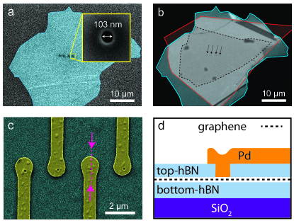
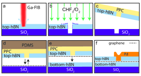
To produce PCs compatible with high mobility graphene we have fabricated four equally spaced holes in the top hBN layer of hBN-graphene-hBN hetero-structures. In order not to damage the graphene, the top-hBN layer (10-20 nm thick) was pre-patterned on a separate SiO2 wafer using a gallium based focused ion beam (Ga-FIB, see details in supporting) prior to the dry-stacking of the heterostructure (Wang13, ; wangWSe2, ). In contrast to establishing the holes with conventional e-beam lithography and subsequent etching, the drilled holes are better defined in shape and the diameter can be adjusted more reliably. In our samples we use a hole-diameter of approximately 100 nm as it is shown in Fig. 1a. Before picking-up the top-hBN from the SiO2 wafer, it is briefly exposed to a CHF3/O2 plasma treatment as without the plasma the flakes are pinned to the SiO2 and pick-up is not possible.
The top-hBN flake is transferred from the SiO2 substrate to a 1 m thick poly-propylene-carbonate (PPC) polymer by spinning the PPC directly onto the SiO2 chip containing the top-hBN with the holes and then peeling the polymer off. The remaining assembly procedure of the hBN-graphene-hBN heterostructure follows the dry-stacking approach proposed by L. Wang et al. (Wang13, ). Since only the top side of hBN comes in contact with the polymer, the method preserves the clean fabrication of dry-stacking graphene. The bottom hBN flake is exfoliated to the target wafer directly, with typical thickness of 20-30 nm.
We use a strongly doped Si++/SiO2 wafer with a 300 nm thick oxide to gate our devices. The final stack was annealed in forming gas at =300 ∘C for 3 hours in order to reduce strain and maximize the areas without bubbles Haigh2012 . A contrast adjusted optical image of the annealed stack is shown in Fig. 1b. The 100 nm thick palladium (Pd) contacts are established using standard e-beam lithography and e-gun evaporation. A false color SEM image of the contact area is shown in Fig. 1c. A schematic of the cross-section of the stack with contacts, as indicated with the dashed pink line in Fig. 1c, is shown in Fig. 1d. Further details of the fabrication are given in the Supporting Material.
In total 4 different samples were produced all showing a similar behaviour. The measurements were performed at cryogenic temperatures (1.5-4 K) using standard low-frequency lock-in technique.
In the following, first the contact resistance and the field-effect measurements at zero magnetic field are discussed. In the second part, the behaviour of the devices at high magnetic field perpendicular to the graphene plane is presented. For the calculation of the charge carrier mobility, a model fitting the device geometry is introduced. The nomenclature of the various differential resistances is given as , with flows from PC and the voltage measured as the difference between PC and , with .
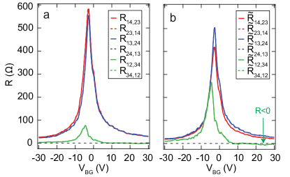
Figure 2a shows for all possible 4-terminal configurations. Out of the six possible configurations, only three are independent: measurements where current- and voltage-probes are inverted are identical as expected from the Onsager relations Onsager31 . The resistance traces show a sharp maximum around zero doping, corresponding to the charge neutrality point (CNP) of graphene.
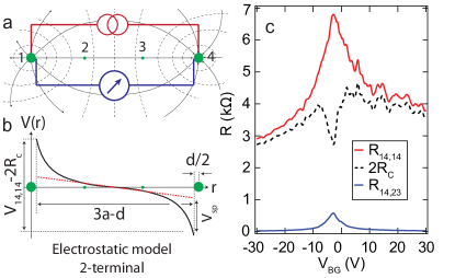
For rectangular graphene devices, where the current density within the graphene sheet is constant, the mobility can be deduced by measuring the field effect of the longitudinal resistance , taking the length and width of the Hall bar into account. For PCs, which are situated in the middle of the graphene sheet, a different formula has to be used since the current density within the graphene sheet varies. Here we introduce a model to extract the sheet conductivity () from the 4-terminal measurement of the resistance, assuming an infinite graphene sheet with a constant . The four contacts are at positions with and diffusive transport. Starting from a single PC at position , the current spreads isotropically into the graphene. This leads to a current density of at distance away from the PC, where is the current. According to , the electric field, , leading to an electrostatic potential . Assuming a current flow between two PCs from , the potential at position is obtained by the superposition principle:
| (1) |
where C is an integration constant. In the 4-terminal measurement only the voltage difference between the two leads at position and () is measured. For simplicity we assume that the voltage probes do not influence the electric field pattern in graphene as shown in Fig. 3a and b. This leads to
| (2) |
where the conductivity can now be extracted from the measurement.
Using can be deduced. The mobility, of the graphene was then extracted using the linear dependence of on the carrier density, (). The density was calculated from the back gate voltage using a parallel plate capacitor model. The hole and electron doped region revealed mobilities of 35’000 cm2/(Vs) and 25’000 cm2/(Vs) respectively. This is in good agreement with the conversion extracted from the evolution of the filling factors in a quantum Hall experiment (QHE) (see supplementary information). An alternative way to determine the mobility is by the onset of the Shubnikov de Haas (SdH) oscillations in the QHE measurement. According to , where is the cyclotron frequency and is the scattering time, the charge carriers can complete a full cyclotron orbit before being scattered. With the SdH oscillations starting at 0.4-0.5 T, a corresponding mobility of 20’000-25’000 cm2/(Vs) is extracted which is in good agreement with the values deduced from the field effect measurements.
Confirmation that a single layer graphene (SLG) is encapsulated in hBN was given by the observed sequence of filling factors in magnetic field (see supplementary information) and by Raman spectroscopy (see supplementary information).
From Eq. 2 it follows that in case of a homogeneous , all 4-terminal resistance measurements can be renormalized according to
| (3) |
With all four contacts at equidistant spacing the logarithm in Eq. 3 simplifies to ln(4), ln(3) or ln(3/4) depending on the measurement configuration. If the model with all the assumptions is valid, all should be equal and given by . The difference between the original and renormalized values can be seen in Fig. 2a and 2b, respectively.
The renormalized values in Fig. 2b are not exactly overlapping, as would be expected for a perfect system given in Eq. 3. However, one can see that the non-local measurements (voltage probes outside the current path), shown in green, which were in the original data smaller by a factor of 7.5 (8) from the blue (red) curve, deviates now only by a factor of 2 (1.6) after renormalization. On the other hand, the local measurements, the blue and red curves are in rather good agreement before and after renormalization. Overall, the rescaled are much closer to each other than the unscaled ones, which confirms that our theoretical model is realistic.
The deviations from the ideal case can be related to the boundary conditions assumed for the model. The most significant deviations from the ideal model are probably i) the finite dimensions of the metallic PCs and ii) the finite size of the graphene sheet, which both change the electric field pattern. Besides that, the sheet conductivity does not seem to be fully uniform within the sample as can be seen by the slight shift of the charge neutrality point between several measurements. The charge neutrality points are at =-2.6 V, -2.8 V and -4.8 V, respectively. Moreover, a non-uniformity of the doping profile arises also from the screening of the top contacts. This results in different lever arms of the back-gate for regions covered and not-covered by the electrodes. Finally, Eq. 3 was derived assuming a completely diffusive sample. However, the charge carriers in the sample are most likely in an intermediate regime between the diffusive and the ballistic regime.
Using the Drude formula, the scattering mean free path can reach 1m at V, which is in the same order as the contact distance m. In this intermediate regime it can occur that the voltage drop over a larger, but clean (ballistic) area is lower compared to a smaller, but dirty (diffusive) area. Moreover, for ballistic trajectories the probability of arriving at a contact, which is farther away can be higher. This picture explains the negative resistance at certain doping values observed in the non-local measurement indicated with an arrow in Fig. 2c. For all the configurations where the voltage-probes are (at least partially) within the current path, the bias voltage will be dominant and consequently no negative signal can be seen.
.
In order to extract the contact resistance which arises between the metal leads and the graphene, (interface resistance), we turn to two terminal measurements. To calculate the contact resistance we measure the 2-terminal resistance between the outer contacts (1,4) as sketched in Fig. 3a. Then the contact resistance can be calculated according to:
| (4) |
where is the intrinsic graphene resistance including a geometry factor (which will be evaluated in the following) and . Here we assumed the same contact resistance for the two contacts. Due to the higher electric field near the source and drain contacts, shown in Fig. 3a, the voltage changes faster near them. This can be seen in Fig. 3b, where the potential along the line connecting the contacts is plotted.
The resistance coming from the non-linearity of the potential near the contacts is called spreading resistance and leads to a potential difference that is marked as in Fig. 3b Zhang12 . It is of the same origin as Maxwell’s resistance that occurs in metallic point contacts Maxwellbook .
To calculate the geometrical factor , we use Eq. 2, and apply it together with Eq. 4 to the situation sketched in Fig. 3a. Because the potential is singular at position and we introduce a cut-off for the potential at away from the singularity, where is the diameter of the contact. Physically speaking this accounts for the equipotential within the metallic PCs with a finite dimension. Doing so, both terms in the numerator and denominator of Eq. 2 become and respectively, where is the distance in between two neighbouring contacts. This leads to
| (5) |
Using where the geometrical factor becomes:
| (6) |
In Fig. 3c the extracted contact resistance is shown using a geometry factor of =7.04 (=2.2 m and =100 nm). The contact resistance of different contact configurations and different devices is of the order of Rc=0.5-1.5 k at high doping. This value is quite remarkable for PCs of only 100 nm in diameter since as well top-contacts with significantly larger areas (in the order of m2) have resistances in the k range. Moreover, the presented model shows that the contact resistance at high doping is given roughly by the 2-terminal resistance at high doping (=30 V). In this case graphene becomes very conductive and the voltage-drop over the graphene is minimal, therefore .
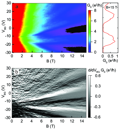
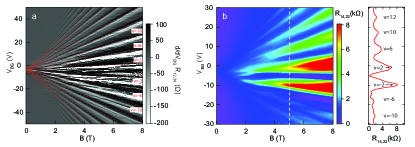
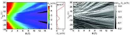
To further characterize the PCs, we have applied a magnetic field perpendicular to the graphene sheet, which forces the charge carriers to move along cyclotron orbits. With a sufficiently high magnetic field the device is driven into the quantum Hall regime, into a state, where the bulk of the sample is insulating, since charge carriers will be localized either around the PCs or along the edges of the sample, which decouples the PCs from each other and the edge of the sample. In the case of a homogenously doped and gated device one would expect complete insulation as soon as the cyclotron orbit and the magnetic length are smaller than the distance between the PCs. The latter is the case for magnetic fields in the few hundred mT range. Moreover is required.
The conductance as a function of back-gate and magnetic field of a sample with a hole to hole spacing of =1 m and a mobility of 15’000 cm2/(Vs) is shown in Fig. 4. The magnetic field dependence of the device discussed before can be found in the Supporting Information. The black region in Fig. 4a shows values of e2/h (1 M). It can be seen, that by the application of magnetic field the sample becomes insulating, however, the fields required are much higher than expected. From simple considerations above this should happen around T.
Inhomogenous doping distribution in the sample can result in coupling of the contacts. For complete insulation of the device, the graphene has to be simultaneously insulating in the whole region between the contacts, since on the border of regions with different filling factors edge currents will flow. Tunneling to these edge states can give short-cut currents between the contacts. As already mentioned in the text, doping inhomogenities exist within our sample, as can be seen from the shift of the charge neutrality point between different 2T measurements. Furthermore, locally the back-gate can be screened by the top contacts. However, our estimates have shown, that the screening changes the gate efficiency by less than 4% far away from the CNP, where the quantum capacitance is high. Only close to the CNP, where the quantum capacitance is small, does screening of the contacts increase to 20%. Furthermore, an additional offset potential may emerge in the regions of the top contacts due the formation of a contact potential between the palladium contacts and h-BN. We emphasize, that substantial part of the voltage drops in the region close to the contact. The combination of all these effects can cause local differences in the filling factor, which can account for the observed high threshold fields.
In future devices insulation of at lower field can be achieved by choosing devices with smaller doping inhomogenities, which can come from bubbles present in the stacks. Moreover the inhomogenous screening of the top contacts or offset potentials can be circumvented by careful design, in which the flake would be fully covered with a metallic plane to achieve a homogeneous doping situation.
We have shown a new method to establish inner point contacts with dimensions of 100 nm in a hBN-graphene-hBN heterostructure. A simple model has been introduced which qualitatively explains our 2 and 4-terminal gate dependent conductance measurements. Surprisingly low contact resistance Rc=0.5-1.5 k have been found despite the small PC size. Magnetic field measurements showed that the inner contacts are decoupled from the edge and from each other at high magnetic fields.
The presented technique is compatible with high-quality encapsulated graphene, since the hBN flake is patterned prior to the stacking and therefore the graphene remains clean. With further optimization one can expect devices with mobilities around 100 000 cm2/(Vs). The technique also holds the potential to further decrease the contact size, since with the Ga-FIB hole diameters below =20 nm are possible.
The point contacts introduced here give the possibility to complement side and top contacts in complex devices and could be the potential milestone towards realizing novel concepts like lensing or measurements of caustics in p-n junctions.
Acknowledgments
This work was further funded by the Swiss National Science Foundation, the Swiss Nanoscience Institute, the Swiss NCCR QSIT, the ERC Advanced Investigator Grant QUEST, the ERC grant 258789, OTKA grant K112918 and the EU flagship project graphene.
The authors thank Simon Zihlmann, Srijit Goswami and Ming-Hao Liu for the fruitful discussions.
References
- [1] Peter Rickhaus, Romain Maurand, Ming-Hao Liu, Markus Weiss, Klaus Richter, and Christian Schönenberger. Ballistic interferences in suspended graphene. Nat Commun, 4:–, August 2013.
- [2] Anya L. Grushina, Dong-Keun Ki, and Alberto F. Morpurgo. A ballistic pn junction in suspended graphene with split bottom gates. Appl. Phys. Lett., 102(22):223102, June 2013.
- [3] L.C. Campos, A.F. Young, K. Surakitbovorn, K. Watanabe, T. Taniguchi, and P. Jarillo-Herrero. Quantum and classical confinement of resonant states in a trilayer graphene fabry-perot interferometer. Nat Commun, 3:1239–, December 2012.
- [4] Peter Rickhaus, Péter Makk, Ming-Hao Liu, Endre Tóvári, Markus Weiss, Romain Maurand, Klaus Richter, and Christian Schönenberger. Snake trajectories in ultraclean graphene p-n junctions. Nat Commun, 6:–, March 2015.
- [5] Thiti Taychatanapat, Jun You Tan, Yuting Yeo, Kenji Watanabe, Takashi Taniguchi, and Barbaros Özyilmaz. Conductance oscillations induced by ballistic snake states in a graphene heterojunction. Nat Commun, 6:–, February 2015.
- [6] P Rickhaus, M.-H. Liu, P. Makk, R. Maurand, S. Hess, S. Zihlmann, M. Weiss, K. Richter, and K. Schönenberger. Guiding of electrons in a few-mode ballistic graphene channel. Nano Letters, doi:10.1021/acs.nanolett.5b01877, 0(10.1021/acs.nanolett.5b01877):null, 2015. PMID: 26280622.
- [7] Thiti Taychatanapat, Kenji Watanabe, Takashi Taniguchi, and Pablo Jarillo-Herrero. Electrically tunable transverse magnetic focusing in graphene. Nat Phys, 9(4):225–229, April 2013.
- [8] V. E. Calado, Shou-En Zhu, S. Goswami, Q. Xu, K. Watanabe, T. Taniguchi, G. C. A. M. Janssen, and L. M. K. Vandersypen. Ballistic transport in graphene grown by chemical vapor deposition. Applied Physics Letters, 104(2):–, 2014.
- [9] Naomi Mizuno, Bent Nielsen, and Xu Du. Ballistic-like supercurrent in suspended graphene josephson weak links. Nat Commun, 4, November 2013.
- [10] Victor E. Calado, Srijit Goswami, Gaurav Nanda, Mathias Diez, Anton R. Akhmerov, Kenji Watanabe, Takashi Taniguchi, Teun M. Klapwijk, and Lieven M. K. Vandersypen. Ballistic josephson junctions in edge-contacted graphene. arXiv:1501.06817, 2015.
- [11] M. Ben Shalom, M. J. Zhu, V. I. Falko, A. Mishchenko, A. V. Kretinin, K. S. Novoselov, C. R. Woods, K. Watanabe, T. Taniguchi, A. K. Geim, and J. R. Prance. Proximity superconductivity in ballistic graphene, from fabry-perot oscillations to random andreev states in magnetic field. arXiv:1504.03286, 2015.
- [12] M. T. Allen, O. Shtanko, I. C. Fulga, J. I.-J. Wang, D. Nurgaliev, K. Watanabe, T. Taniguchi, A. R. Akhmerov, P. Jarillo-Herrero, L. S. Levitov, and A. Yacoby. Visualization of phase-coherent electron interference in a ballistic graphene josephson junction. arXiv:1506.06734, 2015.
- [13] A. V. Kretinin, Y. Cao, J. S. Tu, G. L. Yu, R. Jalil, K. S. Novoselov, S. J. Haigh, A. Gholinia, A. Mishchenko, M. Lozada, T. Georgiou, C. R. Woods, F. Withers, P. Blake, G. Eda, A. Wirsig, C. Hucho, K. Watanabe, T. Taniguchi, A. K. Geim, and R. V. Gorbachev. Electronic properties of graphene encapsulated with different two-dimensional atomic crystals. Nano Lett., 14(6):3270, May 2014.
- [14] L. Wang, I. Meric, P. Y. Huang, Q. Gao, Y. Gao, H. Tran, T. Taniguchi, K. Watanabe, L. M. Campos, D. A. Muller, J. Guo, P. Kim, J. Hone, K. L. Shepard, and C. R. Dean. One-dimensional electrical contact to a two-dimensional material. Science, 342(6158):614, November 2013.
- [15] V.G. Veselago. The electrodynamics of substances with simultaneously negatives of and . Sov. Phys. Usp., 10:509, 1968.
- [16] Vadim V. Cheianov, Vladimir Fal’ko, and B. L. Altshuler. The focusing of electron flow and a veselago lens in graphene p-n junctions. Science, 315(5816):1252, March 2007.
- [17] S. Gómez, P. Burset, W. J. Herrera, and A. Levy Yeyati. Selective focusing of electrons and holes in a graphene-based superconducting lens. Phys. Rev. B, 85:115411, March 2012.
- [18] Gil-Ho Lee, Geon-Hyoung Park, and Hu-Jong Lee. Observation of negative refraction of dirac fermions in graphene. arXiv:1506.06281, 2015.
- [19] J. L. Garcia-Pomar, A. Cortijo, and M. Nieto-Vesperinas. Fully valley-polarized electron beams in graphene. Phys. Rev. Lett., 100:236801, Jun 2008.
- [20] Csaba G Péterfalvi, László Oroszlány, Colin J Lambert, and József Cserti. Intraband electron focusing in bilayer graphene. New Journal of Physics, 14:063028, 2012.
- [21] Ali G. Moghaddam and Malek Zareyan. Graphene-based electronic spin lenses. Phys. Rev. Lett., 105:146803, Sep 2010.
- [22] Aavishkar A. Patel, Nathan Davies, Vadim Cheianov, and Vladimir I. Fal’ko. Classical and quantum magneto-oscillations of current flow near a p-n junction in graphene. Phys. Rev. B, 86:081413, August 2012.
- [23] Nathan Davies, Aavishkar A. Patel, Alberto Cortijo, Vadim Cheianov, Francisco Guinea, and Vladimir I. Fal’ko. Skipping and snake orbits of electrons: Singularities and catastrophes. Phys. Rev. B, 85:155433, April 2012.
- [24] Yue Zhao, Paul Cadden-Zimansky, Fereshte Ghahari, and Philip Kim. Magnetoresistance measurements of graphene at the charge neutrality point. Phys. Rev. Lett., 108:106804, March 2012.
- [25] C. R Dean, A. F. Young, I. Meric, C. Lee, L. Wang, S. Sorgenfrei, K. Watanabe, T. Taniguchi, P. Kim, K. L., Shepard, and J. Hone. Boron nitride substrates for high-quality graphene electronics. Nat Nano, 5:722, October 2010.
- [26] P. J. Zomer, M. H. D. Guimarães, J. C. Brant, N. Tombros, and B. J. van Wees. Fast pick up technique for high quality heterostructures of bilayer graphene and hexagonal boron nitride. Applied Physics Letters, 105:013101, 2014.
- [27] Andres Castellanos-Gomez, Michele Buscema, Rianda Molenaar, Vibhor Singh, Laurens Janssen, Herre S J van der Zant, and Gary A Steele. Deterministic transfer of two-dimensional materials by all-dry viscoelastic stamping. 2D Materials, 1:011002, 2014.
- [28] Luca Banszerus, Michael Schmitz, Stephan Engels, Jan Dauber, Martin Oellers, Federica Haupt, Kenji Watanabe, Takashi Taniguchi, Bernd Beschoten, and Christoph Stampfer. Ultrahigh-mobility graphene devices from chemical vapor deposition on reusable copper. Science Advances, 1(6), 2015.
- [29] Joel I-Jan Wang, Yafang Yang, Yu-An Chen, Kenji Watanabe, Takashi Taniguchi, Hugh O. H. Churchill, and Pablo Jarillo-Herrero. Electronic transport of encapsulated graphene and wse2 devices fabricated by pick-up of prepatterned hbn. Nano Letters, 15(3):1898–1903, 2015. PMID: 25654184.
- [30] S. J. Haigh, A. Gholinia, R. Jalil, S. Romani, L. Britnell, D. C. Elias, K. S. Novoselov, L. A. Ponomarenko, A. K. Geim, and R. Gorbachev. Cross-sectional imaging of individual layers and buried interfaces of graphene-based heterostructures and superlattices. Nat Mater, 11(9):764–767, September 2012.
- [31] Lars Onsager. Reciprocal relations in irreversible processes. i. Phys. Rev., 37:405, February 1931.
- [32] Peng Zhang, Y.Y. Lau, and R.S. Timsit. On the spreading resistance of thin-film contacts. IEEE Transactions on Electron Devices, 59(7):1936, 2012.
- [33] J. C. Maxwell. A Treatise on Electricity and Magnetism. Clarendon Press, Oxford, (1904).
I Supplementary
I.1 Fabrication
In order to drill holes into the top-hBN with a gallium based focused ion beam (Ga-FIB) we use an acceleration voltage of 30 keV and the smallest possible current (1.1 pA) in order to obtain highest resolution. The hBN to be patterned was exfoliated on a Si++/SiO2 substrate with a 315 nm thick oxide, using the scotch-tape technique. The chips were previously carefully cleaned using Piranha solution (98% H2SO4 and 30% H2O2 in a ratio of 3:1) since it is the bottom face of the hBN which will later on contact the graphene.
Once an ideal hBN flake (thickness 10-30 nm) is identified by optical microscopy, the Ga-FIB is used to drill several holes into the flake (with diameter 100 nm and a equidistant spacing of 1-2.2 m) as sketched in fig S1a.
Before picking-up the hBN from the SiO2 wafer, it is briefly exposed to a CHF3/O2 plasma (40 sccm/4sccm, 60 mTorr, 60 W, 15 s) as shown in fig. S1b. It turned out that without exposing the hBN flakes to the plasma, the hBN flakes could not be picked-up from the SiO2 substrate. A possible explanation might be that during the drilling of the holes with the Ga-FIB, SiO2 from the wafer is sputtered on the side of the holes which pins the flake to the wafer. The CHF3/O2 plasma removes this layer and allows therefore a successful pick-up of the flake from the SiO2 chip.
To pick-up the top-hBN, the SiO2 chip is spin-coated with 1 m of poly-propylene-carbonate (PPC) and baked at 80 ∘C for 5 minutes. By peeling-off the PPC gently from the substrate (fig. S1c), all hBN flakes are transferred from the SiO2 onto the PPC polymer. Peeling-off the PPC without breaking the hBN flakes works best when slowly releasing the PPC at a low angle from the SiO2 chip (drilled flakes are more likely to break). The PPC with the hBN flake is then placed on a home-made stamp of 0.5 mm PDMS.
The remaining assembly procedure of the hBN-graphene-hBN heterostructure follows the dry-stacking approach proposed by L. Wang et al. as shown in fig. S1d-e. [1]. The 100 nm thick palladium (Pd) contacts are established using standard e-beam lithography and e-gun evaporation. A cross-sectional sketch of the final device is shown in fig. S1f.
I.2 Low field measurements
In a Hall bar configuration, a clear distinction between longitudinal- () and Hall-resistance () can be made. As long as the Fermi energy is in between two Landau levels (LL) while . However, in our sample the situation is more complex due to the absence of a graphene edge which directly couples to the contacts. As all four contacts are situated in a row, a separation between longitudinal- and Hall-resistance is impossible. Therefore, the 4-terminal resistance , shown in fig. S2b, is more complicated to interpret and goes beyond the scope of this studies. The filling factors have been assigned based on a capacitance model.
The evolution of the filling factors with varying back-gate and magnetic field was determined using a non-local measurement as it revealed more pronounced features in the fan-plot. The back-gate voltage to density conversion (, where is the lever-arm of the back-gate) was extracted from the evolution of the filling factors (, where is the filling factor of the LL and is the Planck constant) in the 4-terminal, non-local measurements shown in fig. S2a. The evolution of the filling factors ( 2, 6, 10…) shown in fig. S2b are in good agreement with the expected sequence for single layer graphene, indicated with the red, dashed lines.
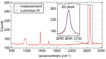
Fitting the full width at half maximum (FWHM) of the 2D-peak in the Raman spectra is an alternative way to determine the exact number of graphene layers present in the device, shown in fig. S3. [2] We extracted a FWHM of 18.3 cm-1 using a single Lorentzian to fit our data which fits much better to the value of single layer graphene (FWHM=27.53.8 cm-1) as compared to bilayer graphene (FWHM=51.7.51.7 cm-1).
I.3 Thermal cycling
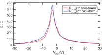
The identical 4-terminal measurement was performed after the first- and second cool-down to obtain some knowledge about a possible degradation due to thermal cycling. As can be seen in fig. S4, almost no change could be observed between the two measurements.
I.4 High field measurements
High-field measurements of another sample with a distance of 2.2 m in between the PCs is shown in fig. S5. It can be seen that the sample becomes insulating between neighbouring contacts at comparable fields as the sample shown in the main article.
The black region in fig. S5a shows the threshold for e2/h (1 M).
References
- [1] L. Wang, I. Meric, P. Y. Huang, Q. Gao, Y. Gao, H. Tran, T. Taniguchi, K. Watanabe, L. M. Campos, D. A. Muller, J. Guo, P. Kim, J. Hone, K. L. Shepard, and C. R. Dean. One-dimensional electrical contact to a two-dimensional material. Science, 342(6158):614, November 2013.
- [2] Yufeng Hao, Yingying Wang, Lei Wang, Zhenhua Ni, Ziqian Wang, Rui Wang, Chee Keong Koo, Zexiang Shen, and John T. L. Thong. Probing layer number and stacking order of few-layer graphene by raman spectroscopy. Small, 6:195, 2010.