Emission and amplification of surface plasmons in resonant - tunneling van der Waals heterostructures
Abstract
We predict a new mechanism of surface plasmon amplification in graphene-insulator-graphene van der Waals heterostructures. The amplification occurs upon the stimulated interlayer electron tunneling accompanied by the emission of a coherent plasmon. The quantum-mechanical calculations of the non-local high-frequency tunnel conductivity show that a relative smallness of the tunneling exponent can be compensated by a strong resonance due to the enhanced tunneling between electron states with collinear momenta in the neighboring graphene layers. With the optimal selection of the barrier layer, the surface plasmon gain due to the inelastic tunneling can compensate or even exceed the loss due to both Drude and interband absorption. The tunneling emission of the surface plasmons is robust against a slight twist of the graphene layers and might explain the electroluminescence from the tunnel-coupled graphene layers observed in the recent experiments.
The ultrarelativistic nature of electrons in graphene gives rise to the uncommon properties of their collective excitations – surface plasmons Grigorenko et al. (2012); Koppens et al. (2011); Jablan et al. (2009). The deep subwavelength confinement Jablan et al. (2009), the unconventional density dependence of frequency Ryzhii et al. (2007); Hwang and Das Sarma (2007), and the absence of Landau damping Ryzhii et al. (2007) are probably the most well-known features of plasmons in graphene-based heterostructures. Among more sophisticated predictions there stand the existence of weakly damped transverse electric plasmons Mikhailov and Ziegler (2007) and quasi-neutral electron-hole sound waves near the neutrality point Svintsov et al. (2012); Gangadharaiah et al. (2008). Some peculiar types of plasmons can be excited in the graphene junctions Mishchenko et al. (2010), field- effect transistors Tomadin and Polini (2013); Svintsov et al. (2013a), optoelectronic modulators Ryzhii et al. (2012), and nanomechanical resonators Svintsov et al. (2014) engaging for the improved device performance at the terahertz frequencies.
Unfortunately, the experimental studies of graphene plasmons are yet unable to confirm or refute many of these predictions. To achieve an extreme plasmon confinement, one has to sacrifice their propagation length. The latter is of the order of several micrometers at the infrared frequencies Fei et al. (2012); Chen et al. (2012) and is limited by the interband absorption in intrinsic samples and somewhat lower Drude absorption in the doped ones Principi et al. (2014). The experimentally reported quality factors of graphene plasmons reach only five for graphene on SiO2 Fei et al. (2012); Chen et al. (2012), and 25 for graphene encapsulated in hexagonal boron nitride Woessner et al. (2014) at room temperature. In the latter case, the damping is due to the scattering by the intrinsic acoustic phonons Principi et al. (2014) and can be suppressed only by lowering the temperature.
Instead of reducing the plasmon loss, it is possible to overcome the damping by introducing the gain medium which can replenish the energy being dissipated upon scattering. This idea has stimulated the re-examination of various ’classical’ plasma instabilities in graphene, including the beam and resistive instabilities Mikhailov (2013), Dyakonov-Shur self-excitation Tomadin and Polini (2013); Svintsov et al. (2013a), and generation due to the negative differential conductance Sensale-Rodriguez (2013). On the other hand, the plasmon gain can be provided by the photogenerated electrons and holes recombining with plasmon emission Dubinov et al. (2011), which opens up the prospects of graphene-based spasers Rana (2008). However, relatively fast nonradiative recombination in graphene Winnerl et al. (2011); Gierz et al. (2015) hinders the practical implementation of those structures.
In this paper, we study the inelastic tunneling in graphene-dielectric-graphene van der Waals heterostructures accompanied by the emission of surface plasmons (SPs), and the possibility of the coherent SP amplification due to the tunneling gain. The inelastic plasmon-assisted tunneling was first observed in the late 70’s; it was shown to be responsible for the light emission from metal-insulator-metal tunneling diodes Lambe and McCarthy (1976). Afterwards, the tunneling excitation of SPs was demonstrated using the scanning probes above the metal surfaces Berndt et al. (1991); Persson and Baratoff (1992); Bharadwaj et al. (2011). However, the possibility of the SP gain due to the tunneling to exceed the loss has been never considered realistic due to the smallness of the tunnel exponent, thus all experiments to date have reported only on the spontaneous SP emission. To achieve large tunneling gain, one needs some resonant feature to compensate the smallness of the tunnel exponent. As an example, such a resonance occurs in the quantum cascade lasers due to the alignment of energy subbands in the neighboring quantum wells Kazarinov and Suris (1972); Faist et al. (1994); Ryzhii et al. (2013). In this paper, we show that the frequency dependence of plasmon tunneling gain in double graphene layer structures also exhibits a strong resonance due to the enhanced interaction between the Dirac electrons having collinear momenta Fritz et al. (2008). In twisted graphene layers, the finite momentum of emitted plasmon can bridge the electron dispersions in the neighboring layers together Mishchenko et al. (2014), which makes the effect of plasmon tunneling emission robust against a slight layer twisting. We also discuss the recent experimental observations of the terahertz emission from the double graphene layer heterostructures Yadav et al. (2015) and address the role of the inelastic-tunneling plasmon excitation in the observed spectra.
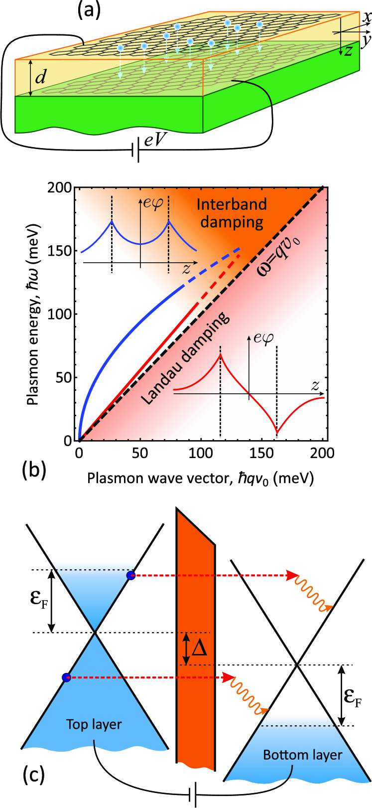
The double-graphene layer heterostructures shown schematically in Fig. 1 a support optical and acoustic surface plasmon modes having symmetric and anti-symmetric distributions of electric potentialHwang and Das Sarma (2009); Svintsov et al. (2013b). Their spectra are studied in detail in the absence of tunneling: the dispersion of symmetric (optical) mode is square-root, , where is the Fermi velocity in graphene, is the Fermi wave vector, is the coupling constant, while the dispersion of the antisymmetric (acoustic) mode is sound-like, (Fig. 1b). Its velocity approaches the Fermi velocity as the interlayer distance decreases, but newer falls below it into the region of Landau damping. In realistic tunnel-coupled double layers ( nm, eV), . Just the acoustic mode has a nonzero average field strength between the two layers and thus can induce interlayer tunneling Das Sarma and Hwang (1998), a process in which an electron passes from one layer to another with emission of a coherent plasmon (Fig. 1 c). The tunneling can be included into the dispersion law of acoustic SPs by considering the tunnel current density as a generation-recombination term in the continuity equations for electrons in a single layer Ryzhii and Shur (2001). In the linear response mode, this current is proportional to the interlayer potential difference, , where is the tunnel conductance. In these notations, the dispersion law of the acoustic SP mode becomes
| (1) |
where is the in-plane conductivity of graphene. Its real part, , is positive and leads to the SP damping. At the same time, can be negative, at least, at low energy of SP quanta . The negative tunnel conductance appears as the number of electrons with the energy in top layer exceeds the number of electrons with energy in the bottom layer; such carrier distribution can be viewed as a ’remote population inversion’. The sign of the quantity thus determines whether the SPs propagating along the double-layer are being damped or amplified.
An only missing ingredient to judge on the possibility of the net plasmon gain is the theory of non-local () high-frequency tunnel conductivity of van der Waals structures; the latter, to the best of our knowledge, has been studied only in the DC limit Brey (2014); Vasko (2013). To construct this theory, we start with the tight-binding Hamiltonian of the tunnel coupled layers in the presence of the propagating plasmon (we set ):
| (2) |
Here, describe separate graphene layers, is the energy spacing between the Dirac points, is the in-plane momentum operator, is the identity matrix, and is the tunneling matrix. For the sake of analytical traceability, we choose in its simplest form which is applicable for AA-stacking of aligned graphene layers Brey (2014); Bistritzer and MacDonald (2011), , where is the ’tunneling frequency’. The interaction part, , describes the electron-plasmon coupling; its matrix elements are calculated as the overlap of the eigen functions of with the electron potential energy in the field of SP , where is the amplitude of potential on the top layer and is the dimensionless ’shape function’ (see Fig. 1 b).
A relatively simple form of the -matrix allows us to treat the tunneling non-perturbatively Vasko and Kuznetsov (2012). The good quantum numbers of the eigen states of are the in-plane electron momentum , the band index ( for the conduction and for the valence band), and an extra index governing the -localization of electron wave function. At large bias voltage, and correspond to the states localized on the top and bottom layers, respectively, while at small bias and describe the anti-symmetric and symmetric states of the tunnel-coupled quantum wells. The eigen energies of these states are
| (3) |
The evaluation of tunnel current density is based on the relation , where is the electron density matrix calculated up to the first order in electron-plasmon interaction, is the spin-valley degeneracy factor, and the indices , run over all quantum numbers. The explicit form of the tunnel current operator is found from the ’equation of motion’, , where is the operator of electron charge in the top layer. The density matrix is found from the von Neumann equation
| (4) |
being interested in the linear response, we commute only the zeroth-order density matrix with . Considering the harmonic time dependence, Eq. (4) is readily solved in the diagonal basis of leading to a closed-form expression for the frequency- dependent non-local tunnel conductance
| (5) |
Here, are the overlap integrals between the SP field profile and the -components of the electron wave functions, , are the overlap factors between the chiral envelope wave functions in graphene, , and are the occupation numbers of the eigen states of given by the Fermi functions shifted by the applied bias in the energy scale.
At this point, it is noteworthy to mention the similarity of Eq. (5) and the expressions for the graphene polarizability Hwang and Das Sarma (2007). The latter diverge on the ’Dirac cone’ as , and a similar singularity appears in the tunnel conductance (5), except the frequency should be replaced with . This singularity is simply elucidated after extracting the real part of Eq. (5) and passing to the elliptic coordinates, which leads us to the following expression
| (6) |
where we have introduced the effective energy shift between the Dirac points , and a dimensionless non-singular function appearing as a result of the Fermi distribution integration,
| (7) |
The real part of the tunnel conductance is negative provided , which implies that the tunneling electrons rather loose their energy by emitting a plasmon than get the energy by plasmon absorption. At the same time, the tunnel transitions from top layer to the bottom one accompanied by SP absorption are prohibited by the energy conservation law as far as the SP velocity exceeds the Fermi velocity. Still, just like in most tunnel phenomena, the negative conductivity due to the tunneling is proportional to a small exponent ( is the decay constant of the electron wave function) that eventually enters and . To enhance the negative conductance, the materials with small effective (tunneling) mass and small band offset with respect to graphene have to be used. Boron nitride ( eV, ) is not the best candidate for the realization of the net SP gain, while chalcogenides of molybdenum MoS2 ( eV, ) and tungsten WS2 ( eV, ) Shi et al. (2013) demonstrate significantly stronger tunneling.
The smallness of tunnel current is to a considerable extent compensated by a singularity in plasmon gain, which occurs provided . The structure of the -integral in Eq. (5) shows that the singularity comes from the tunneling between electron states with collinear momenta in the neighboring layers. Once the carrier dispersion is linear, these states have the same velocity and thus interact for an infinitely long time Fritz et al. (2008). The carrier scattering naturally destroys this coherence making the singular tunnel conductance finite. To account for this effect quantitatively, we add the imaginary self-energy corrections to the quasi-particle energies in (5). These corrections appear as a result of electron-phonon scattering, the latter also leading to the finite Drude absorption. For simplicity, we take to be energy- and momentum independent and equal to its value at the Fermi-surface ,
| (8) |
where eV is the deformation potential of graphene Bolotin et al. (2008), kg/m2 is its mass density, and is the sound velocity Vasko and Ryzhii (2007).
To judge on the possibility of the net plasmon gain, one has also to evaluate the frequency-dependent non-local in-plane conductivity, . In the absence of electron collisions, one can readily apply the Kubo linear response theory and obtain the well-known result including inter- and intraband contributions Falkovsky and Varlamov (2007). The real part of interband optical conductivity () is universal at high frequencies, . However, at finite wave vector – which is the case of plasmons – the frequency dependence of conductivity becomes more complicated,
| (9) |
The neglect of the spatial dispersion results in an underestimate of and, hence, plasmon damping. This is especially crucial for the acoustic modes which velocity just slightly exceeds the Fermi velocity and the respective interband conductivity is in a dangerous vicinity of the singularity at .
Considering the intraband (Drude) conductivity, a special care should be taken to account correctly both for the spatial dispersion and finite carrier relaxation time Principi et al. (2014). Apparently, the effects of carrier collisions cannot be included by a simple replacement in the Kubo-like expression for the collisionless conductivity Mermin (1970). Even in the quasi-classical formalism of Boltzmann equation (which is justified in the case of interest, , ), the collision integral in the -approximation violates the particle conservation. To avoid those difficulties, we have evalauted the conductivity by solving the kinetic equation with the particle-conserving Bhatnagar-Gross-Krook collision integral Bhatnagar et al. (1954) in the right-hand side. The respective intraband dynamic conductivity reads
| (10) |
where , , and is the collision frequency limited by the electron-phonon scattering Woessner et al. (2014) given essentially by Eq. (8). At zero wave vector, , and we restore the Boltzmann conductivity , while for nonzero the real pat of intraband conductivity typically appears to be larger than its zero- value. This difference between no-local and local conductivities agrees with the experimentally observed distinction between the plasmon lifetime and the Boltzmann relaxation time Woessner et al. (2014).
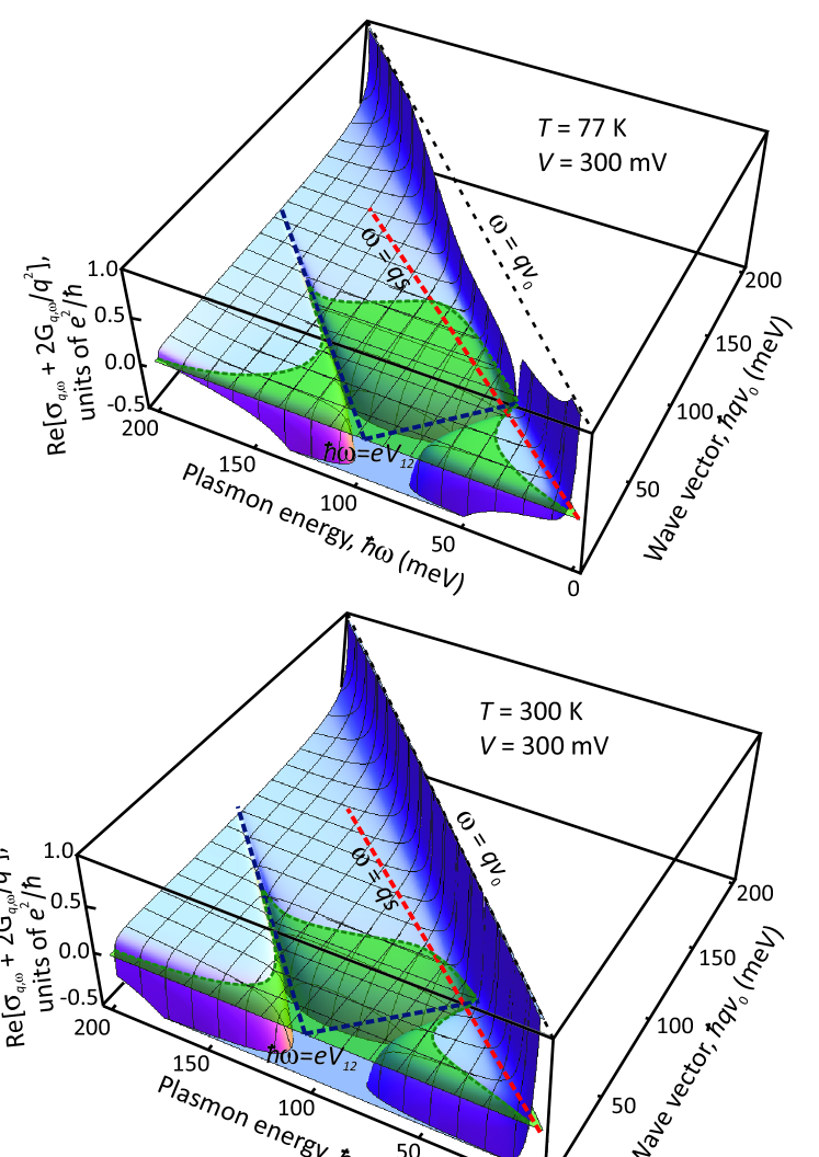
With these prerequisites, we are able to compare the plasmon gain due to the tunneling and loss due to the Drude and interband absorption. Namely, if in some frequency range the ’effective conductivity’ , then the plasmon gain exceeds loss. The self-excitation of plasmons with frequencies satisfying the net gain condition is possible. Figure 2 shows the wave vector- and frequency dependence of the effective conductivity at the room and nitrogen temperatures with the region under the green plane corresponding to the negative values. The two sets of singularities are clearly present in the conductivity spectra: the absorption singularity at comes from the in-plane conductivity, and the gain singularity at comes from the enhanced tunneling between the collinear states. As the wave vector approaches zero, the effective conductance grows indefinitely due to the presence of in the denominator, this will not, however, lead to the infinite plasmon gain as the acoustic SP spectra develop a gap at small wave vectors Das Sarma and Hwang (1998). On the other hand, there is a wide range of frequencies where the dispersion of acoustic SPs in not strongly affected by tunneling, but the real part of net effective conductivity is negative, which justifies the possibility of gain.
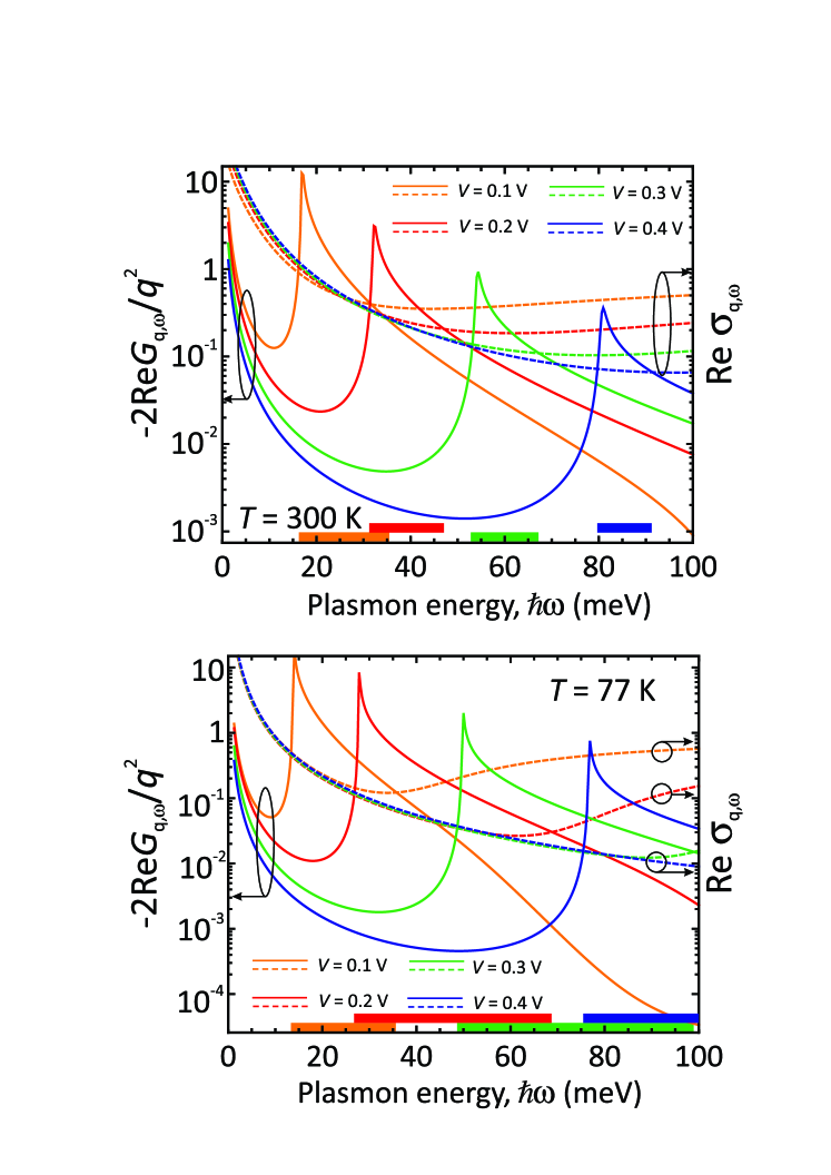
The spectra of in-plane conductivity and effective tunnel conductance are compared in Fig. 3 for the wave vectors satisfying the acoustic plasmon dispersion . At room temperature (upper panel) the self-excitation is possible in a narrow ( meV) vicinity of the tunneling resonance frequency, while at higher frequencies the strong interband absorption surpasses the gain. At lower temperature of 77 K (lower panel) the range of frequencies corresponding to the net SP gain is significantly broader, while the peak tunnel conductance is higher. The broadening of the gain region is due to efficient low-temperature Pauli blocking of the interband transitions with energy below the double Fermi energy. The sharpening of the resonant peak is attributed to the phonon freezing-out at low temperatures, which increases the quasiparticle lifetime and resonant gain. It is also noteworthy that the peak in the negative tunnel conductance occurring at falls into the ’transparency window’ of graphene where the Drude absorption is low () but the interband absorption is still blocked ().
The efficiency of SP excitation can be further improved in the gated double-graphene layer structures, where the energy shift between Dirac points and the carrier density can be controlled independently. At the fixed carrier density, the plasmon gain increases with reduction in as the energies of the and states get closer in energy scale resulting in enhanced tunnel coupling.
In realistic graphene-based tunnel structures, the adjacent layers are always slightly misaligned in real space, which results in the misalignment of Dirac cones in the -space. The finiteness of SP wave vector can, to some extent, compensate this misalignment. If the Dirac cones in adjacent layers are separated by a wave vector , the tunneling resonance will be retained, though the position of the resonant peak will depend on the direction of plasmon propagation . The resonant condition in this case is easily shown to be
| (11) |
and the expressions for the real part of tunnel conductance are obtained from Eq. (6) by a simple replacement . The case of the plasmon-assisted resonant tunneling is thus radically different from the photon-assisted tunneling Ryzhii et al. (2013), where even a slight misalignment breaks the resonance due to the negligible photon momentum. The robustness of SP emission against slight misalignment correlates with the broadness of gain (and emission) spectra extending above the resonant frequency. At the same time, the spectra of phonons emitted upon tunneling are predicted to be Lorentzian their width being limited by the carrier relaxation rate. For these reason, the inelastic tunneling accompanied by the emission of surface plasmons rather than photons may largely contribute to the spontaneous terahertz emission from the double graphene layer structures observed in Yadav et al. (2015). The mechanism of electromagnetic radiation in case of plasmon excitation could be either the dipole radiation of the whole heterostructure, or the radiative decay of plasmons scattered by the edges.
In conclusion, we have theoretically studied the frequency-dependent non-local tunnel conductivity in the biased graphene layers. In a wide range of frequencies, the real part of the tunnel conductivity is negative due to the dominance of inelastic tunneling with surface plasmon emission over the absorption. Moreover, at frequencies satisfying the condition , where is the interlayer potential difference and is the plasmon wave vector, the absolute value of negative tunnel conductivity is resonantly large, which is a manifestation of enhanced tunneling between electron states with collinear momenta in the neighboring layers. A detailed comparison of the surface plasmon loss due to the interband and Drude absorption and gain due to the inelastic tunneling shows the possibility of the net gain in sufficiently thin tunnel structures.
The work of DS was supported by the grant # 14-07-31315 of the Russian Foundation of Basic Research. The work at RIEC was supported by the Japan Society for Promotion of Science (Grant-in-Aid for Specially Promoted Research No. 23000008).
I Appendix
Appendix A Evaluation of the in-plane conductivity
The expression for the interband part of conductivity is readily obtained from the Kubo theory Falkovsky and Varlamov (2007)
| (A1) |
Here is the matrix element of velocity operator in graphene , , is the electron distribution functions in the valence () and the conduction () band, and is the dispersion law in the -th band. Known the eigen functions of graphene Hamiltonian ,
| (A2) |
one readily finds . The subsequent calculations are conveniently performed in the elliptic coordinates
| (A3) |
In these coordinates , . The real part of conductivity is readily extracted with Sokhotski theorem, which leads us to
| (A4) |
To proceed further, we note that in the domain of interest one always has . As a simplest approximation, one can set in the arguments of distribution function and obtain
| (A5) |
The agreement between approximate analytical expression (A5) and exact integral relation (A4) is fair as far as is not too close to . A better agreement can be obtained after the change of variable in Eq. (A4) by noting that varies rapidly over the integration domain , while the remainder varies slowly. Thus, one can make the following approximation
| (A6) |
The following approximation for the conductivity holds
| (A7) |
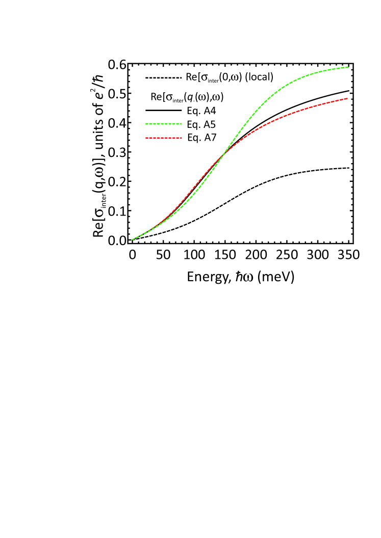
Figure A1 shows the calculated interband conductivities using the exact (A4) and approximate expressions (A5) and (A7) as well as the local () approximation. Clearly, the neglect of spatial dispersion in the case of acoustic SPs with velocity slightly exceeding the Fermi velocity results in an underestimation of the damping.
We now pass to the in-plane conductivity associated with the intraband transitions, . We shall restrict ourselves to the classical description of the intraband electron motion which is justified at frequencies , . The effect of plasmon tunneling gain occurs in this frequency domain, otherwise, the interband damping of SPs takes place [see Eq. 9]. To account for the carrier relaxation in the non-local () case we adopt the formalism of kinetic equation with the particle-conserving Bhatnagar-Gross-Krook collision integral Bhatnagar et al. (1954) in the right-hand side,
| (A8) |
Here is the sought-for field-dependent correction to the equilibrium electron distribution function , is the respective correction to the electron density, is the quasi-particle velocity, and is the electron collision frequency which is assumed to be energy-independent. The current density, associated with the distribution function reads:
| (A9) |
Recalling the relation between small-signal variations of density and current, , and evaluating the integrals in Eq. (A9), we find the conductivity given by Eq. (10).
Appendix B Spectra of plasmons coupled to the double graphene layer heterostructures
The plasmon spectra are obtained by a self-consistent solution of the Poisson’s equation
| (A10) |
the continuity equations
| (A11) |
and the linear-response relation between current density and electric field, . Here is the two-dimensional plasmon wave vector, is the distance between layers, is the background dielectric permittivity, and are the small-signal variations of charge density in the top and bottom layers, respectively. In the absence of built-in voltage, due to the electron-hole symmetry, the charge densities in the layers are equal in modulus an opposite in sign, moreover, the layer conductivities are equal. This allows us to seek for the solutions of Eq. (A10) being symmetric and anti-symmetric with respect to the electric potential. A straightforward calculation brings us to the following dispersions Svintsov et al. (2013b)
| (A12) |
for the antisymmetric (acoustic) mode, and
| (A13) |
for the symmetric (optical mode). Being interested in the long-wavelength limit, , we perform the expansions , . In the same limit, the conductivity is essentially classical, moreover, the interband transitions do not affect the low-energy part of the spectra. With these assumptions, we use the following (collisionless) approximation for the conductivity
| (A14) |
which follows readily from Eq. (10) after setting . Equation (A12) admits an analytical solution, which is a sound-like dispersion
| (A15) |
Here, we have introduced the Fermi wave vector . The velocity of the acoustic mode always exceeds the Fermi velocity thus preventing the Landau damping. The dispersion equation for the optical mode is cubic, however, in the long-wavelength limit the spatial dispersion of conductivity can be neglected as the phase velocity of this mode significantly exceeds the Fermi velocity. The approximate relation for has the following form
| (A16) |
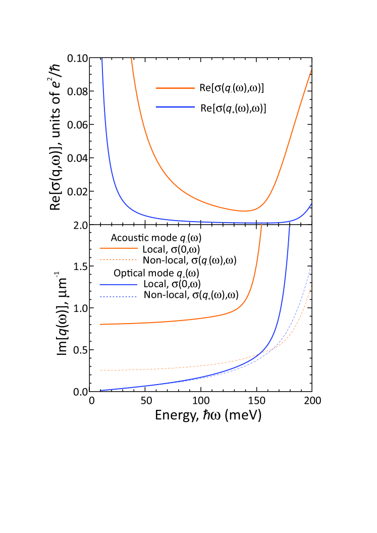
To account for the damping of the propagating plasmon one can express the wave vector from Eqs. (A12) and (A13) and consider the real part of conductivity along with the imaginary one. The results of such calculations are shown in Fig. A2 along with the frequency dependencies of the net conductivity. The acoustic mode is typically damped more heavily than optical one the two effects being responsible for that fact. First of all, the velocity of optical mode is higher than that of acoustic one, hence, at a fixed scattering time, the free path of optical mode is higher. The second reason is the increase in the real part of conductivity at high spatial dispersion discussed above. The use of ’local’ expressions for conductivity results in a factor of two error in the free path of acoustic mode, which is also illustrated in Fig. ( A2).
In the following calculations we shall also require the spatial dependence of the plasmon potential in the acoustic mode, which can be obtained from (A10). It is convenient to present it as
| (A17) |
where is the electric potential on the top layer. The shape function has the following form
| (A18) |
Appendix C Estimate of the effective tight-binding parameters
The tight-binding Hamiltonian of the tunnel-coupled graphene layers in the absence of the propagating plasmon [ in Eq. (2)] constitutes the blocks describing isolated graphene layers and the block describing tunnel hopping . This Hamiltonian acts on a four-component wave function
| (A19) |
which components are the probability amplitudes of finding an electron on a definite layer and on the definite lattice cites, or . Such description of electron states is common for graphene bilayer; moreover, the elements of tunneling matrix have been evaluated for different twist angles between single layers constituting a bilayer. In more comprehensive theories, the -matrix is affected by the band structure of dielectric layer. Here, for the sake of analytical traceability, we choose the tunneling matrix in its simplest form which is applicable to the AA-stacked perfectly aligned graphene bilayer, , where can be interpreted as the tunnel hopping frequency.
To estimate its value, we switch for a while from the tight binding to the continuum description of electron states in the -direction. We model each graphene layer with a delta-well , where is the potential strength chosen to provide a correct value of electron work function from graphene to the background dielectric,
| (A20) |
where is the effective electron mass in the dielectric. The effective Schrodinger equation in the presence of voltage bias between graphene layers takes on the following form
| (A21) |
where is the potential energy created by the applied field
| (A22) |
The solutions of effective Schrodinger equation represent decaying exponents at , and a linear combination of Airy functions in the middle region
| (A23) |
where is the dimensionless energy and is the effecive length in the electric field. A straightforward matching of the wave functions at the graphene layers yields the dispersion equation
| (A24) |
where is the decay constant of the bound state wave function in a single delta-well, , Equation (A24) yields two energy levels () which cannot be expressed in a closed form via the parameters of the well. However, the dependence of on the energy separation between layers is accurately described by
| (A25) |
The energy spectrum (A25) is typical for the tunnel coupled quantum wells Vasko and Kuznetsov (2012); the same functional dependence of energy levels on is naturally obtained by diagonalizing the block Hamiltonian (2),
| (A26) |
This allows us to estimate the tunnel coupling as half the energy splitting of states in double graphene layer well in the absence of applied bias
| (A27) |
The -index governs the -localization of electron in a biased double quantum well. At large bias , the delta-wells interact weakly, thus corresponds to the state localized almost completely in the top layer and corresponds to the electron in the bottom layer. At small bias the state is anitisymmetric and is symmetric.
Appendix D Electron-plasmon interaction and solution of the von Neumann equation
The presence of plasmon propagating along the double graphene layer results in an additional potential energy of electron
| (A28) |
where we assume the direction of plasmon propagation to be along the -axis, and the dependence of potential on the -coordinate is given by Eqs. (A17) and (A18). The additional terms in Hamiltonian due to the vector-potential are negligible as far as the speed of light substantially exceeds the plasmon velocity.
With our choice of the tight-binding basis functions (A19) as those localized on a definite layer and on a definite lattice cite, we shall require 16 matrix elements of the potential energy (A28) connecting those basis states. However, it is more convenient to work out the matrix elements of (A28) connecting the eigen states of Hamiltonian (2). The good quantum numbers of these states are the in-plane momentum , the band index ( for the conduction band and for the valence band) and the - index discussed above. The respective matrix elements are
| (A29) |
Having obtained the matrix elements of electron-plasmon interaction, we pass to the solution of the von Neumann equation (4). Being interested in the linear response of electron system to the plasmon field, we decompose the density matrix as , where is linear in the electron-plasmon interaction . The calculations are conveniently performed in the basis of the eigenstates of including the effects of tunneling non-perturbatively. In this basis, , and thus one readily writes down the solution for the density matrix
| (A30) |
The first-order correction is now expressed through the density matrix in the absence of plasmon field . A particular choice of requires the solution of kinetic equation in the voltage-biased tunnel-coupled layers, however, in several limiting cases the situation is greatly simplified Kazarinov and Suris (1972). If the tunneling rate is slower than the electron energy relaxation rate (e.g., due to phonons and carrier-carrier scattering), the quasi-equilibrium distribution function is established in each individual layer. In this situation, is diagonal in the basis formed by the wave functions localized on top and bottom layers its elements being the respective Fermi distribution functions. In the other limiting case, when tunneling is stronger than scattering (), the electron is ’collectivized’ by the two layers, and the density matrix is diagonal in the basis of -eigenstates. For the parameters used in our calculations, meV exceeds the relaxation rate meV, and the latter limiting case is justified. Setting , where is the Fermi distribution function, we find
| (A31) |
References
- Grigorenko et al. (2012) A. Grigorenko, M. Polini, and K. Novoselov, Nat. Photonics 6, 749 (2012).
- Koppens et al. (2011) F. H. L. Koppens, D. E. Chang, and F. J. Garcia de Abajo, Nano Lett. 11, 3370 (2011).
- Jablan et al. (2009) M. Jablan, H. Buljan, and M. Soljacik, Phys. Rev. B 80, 245435 (2009).
- Ryzhii et al. (2007) V. Ryzhii, A. Satou, and T. Otsuji, J. Appl. Phys. 101, 024509 (2007).
- Hwang and Das Sarma (2007) E. H. Hwang and S. Das Sarma, Phys. Rev. B 75, 205418 (2007).
- Mikhailov and Ziegler (2007) S. A. Mikhailov and K. Ziegler, Phys. Rev. Lett. 99, 016803 (2007).
- Svintsov et al. (2012) D. Svintsov, V. Vyurkov, S. Yurchenko, T. Otsuji, and V. Ryzhii, J. Appl. Phys. 111, 083715 (2012).
- Gangadharaiah et al. (2008) S. Gangadharaiah, A. M. Farid, and E. G. Mishchenko, Phys. Rev. Lett. 100, 166802 (2008).
- Mishchenko et al. (2010) E. G. Mishchenko, A. V. Shytov, and P. G. Silvestrov, Phys. Rev. Lett. 104, 156806 (2010).
- Tomadin and Polini (2013) A. Tomadin and M. Polini, Phys. Rev. B 88, 205426 (2013).
- Svintsov et al. (2013a) D. Svintsov, V. Vyurkov, V. Ryzhii, and T. Otsuji, Phys. Rev. B 88, 245444 (2013a).
- Ryzhii et al. (2012) V. Ryzhii, T. Otsuji, M. Ryzhii, V. G. Leiman, S. O. Yurchenko, V. Mitin, and M. S. Shur, J. Appl. Phys. 112, 104507 (2012).
- Svintsov et al. (2014) D. Svintsov, V. G. Leiman, V. Ryzhii, T. Otsuji, and M. S. Shur, J. Phys. D: Appl. Phys. 47, 505105 (2014).
- Fei et al. (2012) Z. Fei, A. Rodin, G. Andreev, W. Bao, A. McLeod, M. Wagner, L. Zhang, Z. Zhao, M. Thiemens, G. Dominguez, M. M. Fogler, A. H. Castro Neto, C. N. Lau, K. F., and D. N. Basov, Nature 487, 82 (2012).
- Chen et al. (2012) J. Chen, M. Badioli, P. Alonso-González, S. Thongrattanasiri, F. Huth, J. Osmond, M. Spasenović, A. Centeno, A. Pesquera, P. Godignon, A. Z. Elorza, N. Camara, F. J. G. de Abajo, R. Hillenbrand, and F. H. L. Koppens, Nature 487, 77 (2012).
- Principi et al. (2014) A. Principi, M. Carrega, M. B. Lundeberg, A. Woessner, F. H. L. Koppens, G. Vignale, and M. Polini, Phys. Rev. B 90, 165408 (2014).
- Woessner et al. (2014) A. Woessner, M. B. Lundeberg, Y. Gao, A. Principi, P. Alonso-González, M. Carrega, K. Watanabe, T. Taniguchi, G. Vignale, M. Polini, J. Hone, R. Hillenbrand, and F. H. L. Koppens, Nat. Mater. (2014).
- Mikhailov (2013) S. A. Mikhailov, Phys. Rev. B 87, 115405 (2013).
- Sensale-Rodriguez (2013) B. Sensale-Rodriguez, Appl. Phys. Lett. 103, 123109 (2013).
- Dubinov et al. (2011) A. A. Dubinov, V. Y. Aleshkin, V. Mitin, T. Otsuji, and V. Ryzhii, J. Phys.: Cond. Mat. 23, 145302 (2011).
- Rana (2008) F. Rana, IEEE T. Nanotechnol. 7, 91 (2008).
- Winnerl et al. (2011) S. Winnerl, M. Orlita, P. Plochocka, P. Kossacki, M. Potemski, T. Winzer, E. Malic, A. Knorr, M. Sprinkle, C. Berger, W. A. de Heer, H. Schneider, and M. Helm, Phys. Rev. Lett. 107, 237401 (2011).
- Gierz et al. (2015) I. Gierz, M. Mitrano, J. C. Petersen, C. Cacho, I. C. E. Turcu, E. Springate, A. Stöhr, A. Köhler, U. Starke, and A. Cavalleri, J. Phys.: Cond. Mat. 27, 164204 (2015).
- Lambe and McCarthy (1976) J. Lambe and S. L. McCarthy, Phys. Rev. Lett. 37, 923 (1976).
- Berndt et al. (1991) R. Berndt, J. K. Gimzewski, and P. Johansson, Phys. Rev. Lett. 67, 3796 (1991).
- Persson and Baratoff (1992) B. N. J. Persson and A. Baratoff, Phys. Rev. Lett. 68, 3224 (1992).
- Bharadwaj et al. (2011) P. Bharadwaj, A. Bouhelier, and L. Novotny, Phys. Rev. Lett. 106, 226802 (2011).
- Kazarinov and Suris (1972) R. Kazarinov and R. Suris, Sov. Phys. Semicond. 6, 148 (1972).
- Faist et al. (1994) J. Faist, F. Capasso, D. L. Sivco, C. Sirtori, A. L. Hutchinson, and A. Y. Cho, Science 264, 553 (1994).
- Ryzhii et al. (2013) V. Ryzhii, A. A. Dubinov, V. Y. Aleshkin, M. Ryzhii, and T. Otsuji, Appl. Phys. Lett. 103, 163507 (2013).
- Fritz et al. (2008) L. Fritz, J. Schmalian, M. Müller, and S. Sachdev, Phys. Rev. B 78, 085416 (2008).
- Mishchenko et al. (2014) A. Mishchenko, J. Tu, Y. Cao, R. Gorbachev, J. Wallbank, M. Greenaway, V. Morozov, S. Morozov, M. Zhu, S. Wong, F. Withers, C. R. Woods, Y.-J. Kim, K. Watanabe, T. Taniguchi, E. E. Vdovin, O. Makarovsky, T. Fromhold, V. Fal’ko, A. Geim, L. Eaves, and K. Novoselov, Nat. Nanotechnol. 9, 808 (2014).
- Yadav et al. (2015) D. Yadav, S. Tombet, T. Watanabe, V. Ryzhii, and T. Otsuji, in 73rd Annual Device Research Conference (DRC) (2015) pp. 271–272.
- Hwang and Das Sarma (2009) E. H. Hwang and S. Das Sarma, Phys. Rev. B 80, 205405 (2009).
- Svintsov et al. (2013b) D. Svintsov, V. Vyurkov, V. Ryzhii, and T. Otsuji, J. Appl. Phys. 113, 053701 (2013b).
- Das Sarma and Hwang (1998) S. Das Sarma and E. H. Hwang, Phys. Rev. Lett. 81, 4216 (1998).
- Ryzhii and Shur (2001) V. Ryzhii and M. Shur, Jpn. J. Appl. Phys. 40, 546 (2001).
- Brey (2014) L. Brey, Phys. Rev. Applied 2, 014003 (2014).
- Vasko (2013) F. T. Vasko, Phys. Rev. B 87, 075424 (2013).
- Bistritzer and MacDonald (2011) R. Bistritzer and A. H. MacDonald, Proc. Nat. Acad. Sci. 108, 12233 (2011).
- Vasko and Kuznetsov (2012) F. T. Vasko and A. V. Kuznetsov, Electronic states and optical transitions in semiconductor heterostructures (Springer Science & Business Media, 2012).
- Shi et al. (2013) H. Shi, H. Pan, Y.-W. Zhang, and B. I. Yakobson, Phys. Rev. B 87, 155304 (2013).
- Bolotin et al. (2008) K. I. Bolotin, K. J. Sikes, J. Hone, H. L. Stormer, and P. Kim, Phys. Rev. Lett. 101, 096802 (2008).
- Vasko and Ryzhii (2007) F. T. Vasko and V. Ryzhii, Phys. Rev. B 76, 233404 (2007).
- Falkovsky and Varlamov (2007) L. A. Falkovsky and A. A. Varlamov, Eur. Phys. J. B 56, 281 (2007).
- Mermin (1970) N. D. Mermin, Phys. Rev. B 1, 2362 (1970).
- Bhatnagar et al. (1954) P. L. Bhatnagar, E. P. Gross, and M. Krook, Phys. Rev. 94, 511 (1954).