Resonant plasmonic terahertz detection in vertical graphene-base hot-electron transistors
Abstract
We analyze dynamic properties of vertical graphene-base hot-electron transistors (GB-HETs) and consider their operation as detectors of terahertz (THz) radiation using the developed device model. The GB-HET model accounts for the tunneling electron injection from the emitter, electron propagation across the barrier layers with the partial capture into the GB, and the self-consistent oscillations of the electric potential and the hole density in the GB (plasma oscillations), as well as the quantum capacitance and the electron transit-time effects. Using the proposed device model, we calculate the responsivity of GB-HETs operating as THz detectors as a function of the signal frequency, applied bias voltages, and the structural parameters. The inclusion of the plasmonic effect leads to the possibility of the HET-GBT operation at the frequencies significantly exceeding those limited by the characteristic RC-time. It is found that the responsivity of GB-HETs with a sufficiently perfect GB exhibits sharp resonant maxima in the THz range of frequencies associated with the excitation of plasma oscillations. The positions of these maxima are controlled by the applied bias voltages. The GB-HETs can compete with and even surpass other plasmonic THz detectors.
I Introduction
Recently, vertical hot-electron transistors (HETs) with the graphene base (GB) and the bulk emitter and collector separated from the base by the barrier layers - the hot-electron graphene-base transistors (GB-HETs) - made of SiO2 and Al2O3 were fabricated and studied 1 ; 2 ; 3 ; 4 . These HETs are fairly promising devices despite their modest characteristics at the present. Similar devices can be based of GL heterostructures with the hBN, WS2, and other barrier layers 5 ; 6 ; 7 ; 8 . The history of different versions of HETs, including those with the thin metal base and the quantum-well (QW) base, in which the carriers are generated from impurities or induced by the applied voltages, as well as HETs with resonant-tunneling emitter, is rather long (see, for example, Refs. 9 ; 10 ; 11 ; 12 ; 13 ; 14 ; 15 ; 16 ). Figure 1 shows schematically the GB-HET structure and its band diagrams. Depending on the GB doping, the base-emitter and collector-base voltages, and , and the thicknesses of barrier layers separating the base from the emitter and collector, and , respectively, the GB can be filled either with electrons or holes [compare Figs. 1(b) and 1(C)].
In GB-HETs (as in HETs) , a significant fraction of the electrons injected from the top n-type emitter contact due to tunneling through the barrier top crosses the GB and reaches the collector, while the fraction of the electrons captured into the GB can be rather small. The tunneling electrons create the emitter-collector current . The variations of the base-emitter voltage result in the variation of .
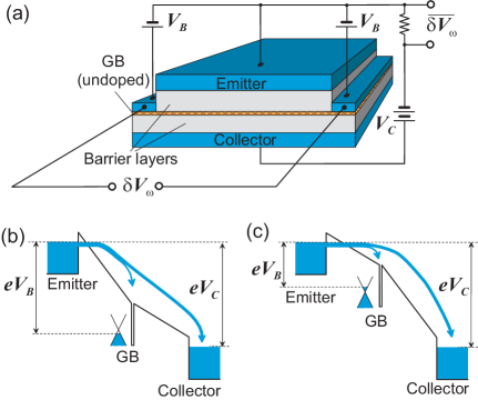
In the case of the GB with a two-dimensional electron gas (2DEG), the GB-HET transistors can also be referred to as the N-n-N heterostructure HETs with the GB of n-type. In another case, when the GB comprises a two-dimensional hole (2DHG), the GB-HET transistors can also be called the N-p-N heterostructure bipolar transistors (HBTs) with the GB of p-type.
The electrons captured into the GB support the emitter-base current . The transistor gain in the common-emitter configuration is equal to , where is the average capture probability of the capture of electrons into the GB during their transit. One of the main potential advantages of GB-HETs is the high-speed operation associated with the combination of a short transit time (due to the vertical structure), a high gain (because of a low probability, , of the hot electron capture into the GB), and a low GB resistance (owing to a high mobility of the carriers in graphene). As shown recently 17 , in the graphene heterostructures with proper inter-graphene barrier layers can be very small. Very small values of in GB-HETs can lead to a fairly high gain. The use of the undoped base with the induced carriers, leads to the exclusion of the scattering of the hot electrons crossing the GB with the impurities and to an increase of the mobility of the carriers localized in the GB.
By analogy with HETs with the QW-base made of the standard materials 18 ; 19 , GB-HETs can exhibit resonant response to the incoming signals associated with the excitation of the plasma oscillations. The resonant plasma frequencies are determined by the characteristic plasma wave velocity (which increases with the carrier density ) and the lateral sizes of the GB , while the quality factor of the plasma resonances is mainly limited by the carrier momentum relaxation time associated with the scattering on impurities, various imperfections, and phonons. Due to the specific features of the carrier statistics and dynamics in the graphene layers 20 , the plasma velocity , where cm/s is the characteristic velocity of the Dirac energy spectrum, and can markedly exceed that in the QW heterostructures. This promotes the realization of with the plasmonic resonances in the terahertz (THz) range even in the GB-HETs with fairly large lateral sizes. The possibility of achieving the elevated carrier mobilities in the GB can enable sharp plasmonic resonances in GB-HETs at room temperatures or above.
The application of the ac voltages at the signal frequency , associated with the incoming radiation (received by an antenna) to the side contacts to the GB, results in the variation of the local ac potential difference (the axis is directed in the GB plane) between the GB and the emitter contact. The emitter, base, and collector current densities , , and include the dc components , , and (determined by the applied bias voltages and ), the ac components , , and (proportional to , and (due to the nonlinear dependence of the tunneling injection current on the local potential difference between the GB and the emitter) the rectified dc components , , and (proportional to , i.e., to the intensity of the incoming radiation received by an antenna. The net rectified current can serve as the output current in the GB-HETs radiation detectors. The detector responsivity . Due to the possibility of the plasmonic resonances, the rectified component (the detector output signal) can be resonantly large, similar to that in the HET detector 21 and other plasmonic THz detectors using different transistor structures, including those incorporating graphene 22 ; 23 ; 24 ; 25 ; 26 ; 27 ; 28 ; 29 ; 30 ; 31 ; 32 ; 33 ; 34 .
In this paper, develop the GB-HET device model and evaluate the GB-HET characteristics as a radiation detector of radiation, in particular, in the THz range of signal frequencies.
II Device model and related equations
We consider a GB-HET with the highly conducting tunneling emitter and collector of the n-type and the undoped GB (as shown in Fig. 1) with a 2DHG induced by the applied bias voltages creating the N-p-N structure with the band diagram shown in Fig. 1(b). The GB-HET device model accounts for the tunneling injection of hot-electrons from the emitter to the barrier layer(above the barrier top), their propagation across the barrier layers, partial capture of hot-electrons into the GB, and the excitation of the self-consistent oscillations of the electric potential and the hole density in the GB (plasma oscillations). The quantum capacitance and the electron transit-time effects are also taken into account.
We assume that the bias voltages and are applied between the GL-base and the emitter and between the collector and the emitter contacts, respectively. In the framework of the gradual channel approximation 35 , which is valid if , the density of the two-dimensional hole gas (2DHG) in the GL-base and its local potential (counted from the potential of the emitter) are related to each other as
| (1) |
where is the dielectric constant of these layers, is the hole charge, is the built-in voltage between the contact material and an undoped GL, and is the 2DHG Fermi energy in the GB. In a degenerate 2DHG, , where is the Planck constant. The dependence of the right side of Eq. (1) on the hole Fermi energy is interpreted as the effect of quantum capacitance 36 ; 37 .
The ac voltages and are applied between the side GB contacts connected with an antenna, so that the ac potential of the GB obeys the following (asymmetric) conditions:
| (2) |
The side contacts can serve as the slot wave guide transforming the incoming THz radiation signals being received by an antenna into the ac voltage [see Fig.1(a)]. The ac component of the collector-emitter voltage can also arise due to the ac potential drop across the load resistance. However, in the GB-HET with the wiring under consideration, can be disregarded providing that the GB-HET structure is symmetrical (see below). For GB-HETs with the degenerate 2DHG, the relation between the variations of the hole density and the potential, and (the ac components) are, as follows from Eq. (1), can be expressed via the net capacitance per unit area , which accounts for the geometrical capacitance (with and being the geometrical emitter and collector capacitances, respectively) and the quantum capacitance 36 ; 37 , where and are the pertinent dc values of the hole density and the Fermi energy.
| (3) |
Considering the electron tunneling from the emitter to the states above the top of the barrier (through the triangular barrier), the emitter electron tunneling current density can be presented as:
| (4) |
Here , is the characteristic tunneling field, is the activation energy for electrons in the contact, is the effective electron mass in the barrier material, is a numerical coefficient, is the electric field in the emitter barrier, and is the maximum current density which can be provided the emitter contact, As follows from Eqs. (2) and (3), the ac component and the rectified component of the emitter tunneling current and (for ) are, respectively, given by
| (5) |
| (6) |
Here , , and are the emitter dc current density (in the absence of the ac signals), the dc electric field in the emitter barrier, and the emitter differential conductance, respectively. The dc hole Fermi energy in the GB obeys the following equation:
| (7) |
The ac electric field components perpendicular to the GB plane in the emitter barrier, as well as in the collector barrier, are respectively given by
| (8) |
| (9) |
Using the Shockley-Ramo theorem, one can find the ac component the electron current densities coming to the base and the collector:
| (10) |
Here
| (11) |
| (12) |
where is the drift velocity of the hot electrons crossing the barriers above their tops (which is assumed to be constant) and and are the electron transit time across the emitter and collector barrier layers. The axis is directed perpendicular to the GB plane. Since under the boundary conditions (2), (see below) and, hence, , the net ac currents
| (13) |
| (14) |
Simultaneously for the rectified components of the dc current densities from the emitter to the GB and from the emitter to the collector one obtains
| (15) |
| (16) |
where
| (17) |
Consequently, the net rectified components of the dc emittter-base and emitter-collector currents are given by
| (18) |
| (19) |
respectively.
The ac hole current along the GB is given by
| (20) |
where the lateral ac conductivity of the GB is given by (see, for example, Refs. 38 ; 39 ; 40 ; 41 ; 42
| (21) |
III Plasma oscillations and rectified current
To calculate the rectified current components using Eqs. (15) and (16), one needs to find the spatial distributions of the ac potentials in the GB .
For this purpose we use the hydrodynamic equations for the hole transport along the GB 43 ; 44 (see also Refs. 21 ; 22 ) coupled with the Poisson equation solved using the gradual channel approximation [i.e., using Eq. (1)]. Linearizing the hydrodynamic equations and Eq. (1) and taking into account that the ac component of the hole Fermi energy is expressed via the variation of their density and the potential, we arrive at the following equation for the ac component of the GB potential (compare with Refs. 16 ; 21 ; 22 which should be solved with boundary conditions given by Eq. (2):
| (22) |
Here is the characteristic velocity of the plasma waves in the gated graphene layers, which is given by 18 , being the so-called ”fictituous” effective hole (electron) mass in graphene layers 27 , and , where is the hole momentum relaxation time in the 2DHG and is associated with the contribution of the 2DHG viscosity to the damping (see for example, Ref. 21 ) and with the radiation damping of the plasma oscillations. The latter mechanism is associated with the recoil that the holes in the GB feel emitting radiation (the pertinent term in the force acting on the holes is referred to as the Abraham-Lorentz force or the radiation reaction force 46 ; 47 ). Taking into account that the viscosity damping rate is proportional to the second spatial derivative, for the gated plasmons with the acoustic-like spectrum ( is the 2DHG viscosity),and considering that 45 ; 46 ; 47 ), we put , where is the pertinent damping parameter, and is the speed of light. If the viscosity damping surpasses the radiation damping, one can set .
The characteristic plasma-wave velocity is determined by (as well as the thicknesses of the emitter and barrier layers and ) 20 and, hence, can be changed by the variations of the bias voltages and . Due to this the characteristic plasmonic frequency can be effectively controlled by these voltages.
Equation (22) with Eq. (2) yield
| (23) |
One can see from Eq. (23) that the spatial dependence of is rather complex. In particular, when approaches to , where , this distribution can be oscillatory with fairly high amplitude of the spatial oscillations when .
Substituting given by Eq. (23) to Eqs. (15) and (16), we arrive at the following:
| (24) |
| (25) |
| (26) |
| (27) |
As follows from Eqs. (24) - (27), and (as for the pertinent dc current in the absence of the THz signals), so that .
Using Eqs. (20) and (24), for the ac current between the based contacts we obtain
| (28) |
Due to the symmetry of the GB-HET structure and the asymmetric spatial distribution of , there is no rectified component of the lateral current in the GB-base, i.e., .
At very low signal frequencies , from Eqs. (23) and (22) we obtain
| (29) |
| (30) |

Since in reality , there is an intermediate range of frequencies . Assuming that , from Eq. (27) we arrive at
| (31) |
If the characteristic frequency of the plasma oscillations , the ac GB potential amplitude can markedly exceed the amplitude of the input ac signal when the frequency is close to one of the resonant plasma frequencies , where is the plasma resonance index. In this case, the rectified emitter-collector current is pronouncedly stratified, i.e., its density is a nearly periodic function of the coordinate .
Figure 2 shows the spatial distributions of the rectified emitter-collector current density (corresponding to the current stratification) calculated for different frequencies using Eq. (25). It is assumed that ps, cm/s, and m. As seen in Fig. 2, the spatial stratification of the current is rather pronounced when is close to the plasma resonant frequencies (the frequencies THz and THz): the current exhibits two streams centered at when THz and four streams centered at when THz. At the frequencies far from the resonances, the spatial current distribution becomes weakly nonuniform.
IV GB-HET detector responsivity
IV.1 Current responsivity
The rectified current can be considered as the output signal used for the detection of electromagnetic radiation (in particular, THz radiation). The current detector responsivity using this output signal is defined as
| (32) |
where is the GB-HET lateral size in the direction along the contacts to the GB, is intensity of the incident radiation, and is the antenna aperture. The latter is given by 50 , where is the antenna gain, is the radiation wavelength, and is the speed of light in vacuum. Taking into account that , where is the radiation electric field in vacuum, and estimating as , one can arrive at
| (33) |
Considering Eqs. (27), (32), and (33), for the current responsivity (in A/W units) we find
| (34) |
where
| (35) |
| (36) |
As follows from Eq. (34), at relatively long hole momentum relaxation times , the GB-HET responsivity exhibits a series of very sharp and high peaks. It is instructive that in the GB-HETs under consideration, the height of the resonant peaks does not decrease with an increasing peak index (as in some other devices using the plasmonic resonances). Although some decrease in the peaks height with the increasing resonance index attributed to the effect of viscosity and radiative damping takes place, the pertinent effect is relatively weak (see below).
In the limiting cases and , corresponding to Eqs. (25) and (26), one obtains
| (37) |
and
| (38) |
respectively. The quantities and depend on the geometrical and quantum capacitances and, therefore, on the barrier layers thicknesses:
| (39) |
For the doping level of the emitter contact cm-3, assuming that the thermal electron velocity cm/s, we obtain A/cm2. Setting eV and the effective mass in the barrier layer g , we arrive at V/cm. Setting also V/cm (to provide the hole density in the GB about of cm-2), we find A/cm2 and Ohm-1cm-1. At these parameters, one obtains also cm-1. Using these data and setting in addition , nm, , and , from Eq. (36) we obtain A/W. If m and m, Eqs. (35) - (36) yield A/W and A/W. These parameters are also used in the estimates below.
In the case of high quality factor of the plasma resonances , the quantities and and, hence, the responsivity as functions of the signal frequency described by Eqs. (27) and (34) exhibit sharp peaks at , attributed to the resonant excitation of the plasma oscillations (standing plasma waves). The peak width is primarily determined by the frequency . Indeed, for Eq. (34) yields
| (40) |
Using the above estimate for , the peak values of the responsivity at THz and ps is approximately equal to max A/W.
Figure 3 shows the dependence of the normalized GB-HET current responsivity calculated using Eq. (34) for several sets of parameters. As seen, the positions of the responsivity peaks shift toward higher frequencies when the plasma frequency increases, i.e., when increases and/or decreases because (compare the curves ”1” and ”2”). A shortening of the momentum relaxation time leads to a smearing of the peaks (compare the curve ”3” corresponding to ps and the curve ”4” corresponding to ps). Figure 4 shows the lowering and broadening of the resonance peaks of the GB-HET current responsivity with the decreasing momentum relaxation time described by Eq. (34). As seen, at ps, the responsivity peaks vanish, while at ps they are fairly sharp and high..
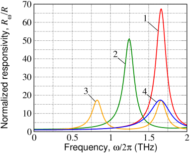
1 - ps, cm/s, m;
2 - ps, cm/s, m;
3 - ps, cm/s, m;
4 - ps, cm/s, m.
These parameters correspond to 5/3, 5/4, 5/6, and 5/3 THz, respectively.

IV.2 Voltage responsivity
The variation of the dc current component cause by the ac signals results in a change of the voltage drop, , across the load resistor in the collector circuit (see Fig. 1). Considering that this leads to an extra variation of the dc emitter and collector currents and because of its dependence on the collector contact dc potential. The latter dependence is essentially associated with the effect of quantum capacitance. Taking this into account, for the voltage responsivity of the GB-HET under consideration we obtain
| (41) |
Here
| (42) |
where is the load resistance. It is instructive that due the the absence of the ac collector current (i.e., the ac current through the load resistor), associated with the GB-HET structure symmetry and the asymmetry of the applied ac signal voltage and the ac potential spatial distribution along the GB) the RC-factor of the voltage responsivity is independent of the signal frequency.
For , Eqs. (38) and (40) yield
| (43) |
At , Eq. (43) yields the obvious formulas:
| (44) |
at low frequencies, and
| (45) |
at the plasma resonance .
At , from Eq. (43) we obtain, respectively,
| (46) |
and
| (47) |
For ps, cm/s, and m (as for the curve ”1” in Fig. 3), so that THz, as well as A/V cm cm-1 (see the estimate in the previous subsection), and from Eq.(47) we obtain the following estimate: . For the above parameters one obtains Ohm. Even at smaller , the voltage responsivity can be fairly large. Setting Ohm, we obtain V/W and V/W, respectively.
Considering Eqs. (42) and (39), we find the following dependences of the current and voltage responsivities and on the emitter and collector barriers thickness (at not too large ):
| (48) |
According to Eq. (48), and markedly decrease in the range nm.
V Discussion
As follows from Eqs. (34) and(40), an increase in with increasing frequency due to the reinforcement of the plasma oscillation damping associated with the viscosity and the radiative damping, might lead to the gradual lowering of the resonant peaks with their index . However, our estimates show that the contribution of these two mechanisms to the net damping is small compared to the damping associated with the hole momentum relaxation (collisional damping). Indeed, disregarding the radiative damping and assuming the 2DHG viscosity to be cm2/s (i.e., smaller than in the standard 2DEG and 2DHG in the GaAs based heterostructures 21 ; 49 ; 50 ) and cm/s, we obtain s. Hence, in the frequency range THz (as in Fig. 2), we find s-1 . Therefore, the heights of the responsivity peaks in Fig. 2 in the curve ”3” at and 1.6 THz are virtually equal. However, the peaks corresponding to higher resonances with the frequencies in the range 5 - 10 THz can be markedly lowered and smeared, because in this range can become comparable with . For example, for the same values of , ps, and = 5 - 10 THz, we obtain .
Equation (42) describes the saturation of the voltage responsivity peak value with increasing load resistance . This is associated with the effect of the voltage drop across the load on the potential drop between the emitter and the base and, hence, the hole Fermi energy in the GB, which determine the injection current. Such an effect is due to the finite value of the GB quantum capacitance (see, Refs. 12 ; 13 ) - if tends to infinity, the emitter-base voltage becomes independent of , and the saturation of the dependence vanishes.
The THz detectors using a similar operation principle and InP double heterojunction bipolar transistors (DHBTs) were recently fabricated and studied experimentally 51 ; 52 ; 53 . The estimated responsivities of the DHBTs in question for the non-resonant detection regime are somewhat smaller but of the same order of magnitude than those given by Eq. (43) and the pertinent estimates. However, the experimental values of the responsivity are much smaller than the values predicted above for the resonant detection [see Eqs. (44) and (46) and the estimates based on these equations]. Apart from the parasitic effects and the absence of any spatial coupling antenna, this can be attributed to the doping of the base in the InP-DHBTs, which inevitably leads to relatively a shorter hole momentum relaxation time compared to that in the GB (where the 2DHG is induced by the applied voltages). Possibly, a higher probability of the hot electron capture into the InGaAs base (that had a relatively large thickness of 28 nm) in the DHBTs in comparison with the GB-HETs can be an additional factor.
The GB-HET current and voltage responsivities are determined by several characteristics: the characteristics of the tunneling emitter, geometrical characteristics of the GB-HET structure, materials of the emitter as well as the emitter and collector barrier layers, and applied bias voltages. The diversity of these factors enables the optimization of the GB-HETs operating as resonant plasmonic detectors, in particular, an increase in the responsivity in comparison with the values obtained in the above estimates. The resonant plasmonic THz detectors can based on not only the GB-HET structure shown in Fig. 1(a) (with an extra antenna connected to the GB side contacts), but also based on lateral structures with the GB contacts forming a periodic array.
The comparison of the GB-HETs 1 ; 2 ; 3 ; 4 and InP-DHBTs 51 ; 52 ; 53 with the GB-HETs under consideration highlights the following advantages of the latter: (i) a longer momentum relaxation time of holes in the GB; (ii) a higher plasma-wave velocity that enables higher resonant plasma frequencies; (iii) a smaller capture probability of hot electrons into the GB and, consequently, larger (or even much larger) fraction of the hot electrons reaching the collector; (iv) coupling the incoming THz signal to the GB resulting in the absence of the ac current in the emitter-collector circuit and prevanting the RC effects usually hindering the high-frequency operation.
VI Conclusions
We developed an analytical model for vertical heterostructure HETs with the GB of the p-type sandwiched between the wide-gap emitter and collector layers and the N-type contacts. Using this model, we described the GB-HET dynamic properties and studied the GB-HET operation as detectors of THz radiation. The main features of the GB-HETs are high hole mobility in the GB, low probability the capture of the hot electrons injected from the emitter and crossing the GB, and the absence of the collector ac current. These features enable pronounced voltage-controlled plasmonic response of the GB-HETs to the incoming THz radiation, high hot-electron injection efficiency, and the elimination of the RC-limitations leading to elevated the GB-HET current and voltage responsivities in the THz range of frequencies, particularly at the plasmonic resonances at room temperature. This might provide the superiority of the GB-HET-based THz detectors over other plasmonic THz detectors based on the standard heterostructures . Thus, the THz detectors based on the GB-HETs can be interesting for different applications.
Acknowledgments
The authors are grateful to D. Coquillat and F. Teppe for the information related to their experimental data on InP HBTs operating as THz detectors. The work was supported by the Japan Society for Promotion of Science (Grant-in-Aid for Specially Promoted Research 23000008) and by the Russian Scientific Foundation (Project 14-29-00277). The works at UB and RPI were supported by the US Air Force award FA9550-10-1-391 and by the US Army Research Laboratory Cooperative Research Agreement, respectively.
References
- (1) W. Mehr, J. Ch.Scheytt, J. Dabrowski, G. Lippert, Y.-H.Xie, M. C. Lemme, M. Ostling, and G. Lupina, IEEE Electron Device Lett. 33, 691, (2012)
- (2) B. D. Kong, C. Zeng, D. K. Gaskill, K.L. Wang, K. W. Kim, Appl. Phys. Lett. 101, 263112 (2012).
- (3) S. Vaziri, G.Lupina, C. Henkel, A. D. Smith, M.Ostling, J. Dabrowski, G. Lippert, W. Mehr, and M. C.Lemme Nano Lett. 13, 1435 (2013).
- (4) C. Zeng, E. B. Song, M. Wang, S. Lee, C. M. Torres,Jr., J. Tang, B. H. Weiler, and K. L. Wang. Nano Lett. 13, 2370 (2013).
- (5) L. Britnel, R. V. Gorbachev, R. Jalil, B.D . Belle, F.Shedin, A. Mishenko, T. Georgiou, M. I. Katsnelson, L. Eaves, S. V. Morozov, N. M. R. Peres, J. Leist, A. K. Geim, K. S. Novoselov, and L. A. Ponomarenko, Science, 335, 947 (2012).
- (6) T. Georgiou, R. Jalil, B. D. Bellee, L. Britnell, R. V. Gorbachev, S. V. Morozov, Y.-J. Kim, A. Cholinia, S. J. Haigh, O. Makarovsky, L. Eaves, L. A. Ponimarenko, A. K. Geim, K. S. Nonoselov, and A. Mishchenko, Nature Nanotechnology 8, 100 (2013).
- (7) L. Britnel, R. V. Gorbachev, A. K. Geim, L. A. Ponomarenko, A. Mishchenko, M. T. Greenaway, T. M. Fromhold, K. S. Novoselov, and L. Eaves, Nature Comm. 4, 1794 (2013).
- (8) M. Liu, X. Yin, and X. Zhang, Nano Lett. 12, 1482 (2012).
- (9) C. A. Mead, Proc. IRE, 48, 359 (1960).
- (10) J.M. Shannon, IEE J. Solid-State Electron Devices, 3, 142 (1979).
- (11) M. Heiblum, D. C. Thomas, C. M. Knoedler, M. I. Nathan, Surf. Sci. 174, 478 (1986).
- (12) S. Luryi, IEEE Electron Device Lett. 6, 178 (1985).
- (13) S. Luryi, inHigh Speed Semiconductor Devices, edited by S. M. Sze (Wiley, New York, 1990), p.399.
- (14) J. Xu and M. S. Shur, Double Base Hot Electron Transistor, United States Patent 4,901,122, February 13 (1990).
- (15) M. S. Shur, R. Gaska, A. Bykhovski, M. A. Khan, and J. W. Yang, Appl. Phys. Lett. 76, 3298 (2000).
- (16) M. Asada, et.al. Jpn. J. Appl. Phys. 47, 4375 (2008).
- (17) V. Ryzhii, T. Otsuji, M. Ryzhii, V. Ya. Aleshkin, A. A. Dubinov, V. Mitin, and M.S.Shur, J. Appl. Phys. 117, 154504 (2015).
- (18) V. Ryzhii, Appl. Phys. Lett. 70, 2532 (1997).
- (19) V. Ryzhii, Jpn. J. Appl. Phys. 37, 5937 (1998).
- (20) V. Ryzhii, A. Satou, and T. Otsuji, J. Appl. Phys. 101, 024509 (2007).
- (21) M. I. Dyakonov and M. S. Shur, IEEE Trans. Electron Devices, 43, 1640 (1996).
- (22) W. Knap, Y. Deng, S. Rumyantsev, J.-Q. Lu, M. S. Shur, C. A. Saylor, and L. C. Brunel, Appl. Phys. Lett. 80, 3433 (2002).
- (23) X. G. Peralta, S. J. Allen, M. C. Wanke, N. E. Harff, J. A. Simmons, M. P. Lilly, J. L. Reno, P. J. Burke, and J. P. Eisenstein, Appl. Phys. Lett. 81, 1627 (2002).
- (24) T. Otsuji, M. Hanabe and O. Ogawara, Appl. Phys. Lett. 85, 2119 (2004).
- (25) J. Lusakowski, W. Knap, N. Dyakonova, L. Varani, J. Mateos, T. Gonzales, Y. Roelens, S. Bullaert, A. Cappy and K. Karpierz, J. Appl. Phys. 97, 064307 (2005).
- (26) F. Teppe, W. Knap, D. Veksler, M. S. Shur, A. P. Dmitriev, V. Yu. Kacharovskii, and S. Rumyantsev, Appl. Phys. Lett. 87, 052105 (2005).
- (27) V. Ryzhii, A.Satou, W.Knap, and M.S.Shur. J. Appl. Phys. 99, 084507 (2008).
- (28) A. El Fatimy, F. Teppe, N. Dyakonova, W. Knap, D. Seliuta, G. Valusis, A. Shcherepetov, Y. Roelens, S. Bollaert, A. Cappy, and S. Rumyantsev, Appl. Phys. Lett. 89, 131926 (2006).
- (29) J. Torres, P. Nouvel, A. Akwaoue-Ondo, L. Chusseau, F. Teppe, A. Shcherepetov, and S. Bollaert, Appl. Phys. Lett. 89, 201101 (2006).
- (30) S.A. Boubanga Tombet, Y. Tanimoto , A. Satou , T. Suemitsu , Y. Wang , H. Minamide , H. Ito, D. V. Fateev , V.V. Popov , and T. Otsuji, Appl. Phys. Lett., 104, 262104 (2014).
- (31) Y. Kurita, G. Ducournau, D. Coquillat, A. Satou, K. Kobayashi, S.A. Boubanga-Tombet, Y.M. Meziani, V.V. Popov, W. Knap, T. Suemitsu, and T. Otsuji Appl. Phys. Lett., 104, 251114 (2014).
- (32) L. Vicarelli, M. S. Vitiello, D. Coquillat, A. Lombardo, A. C. Ferrari, W. Knap, M. Polini, V. Pellegrini, and A. Tredicucci, Nature Mat. 11, 865 (2012).
- (33) V. Ryzhii, T. Otsuji, M. Ryzhii, and M. S. Shur, J. Phys. D: Appl. Phys. 45, 302001 (2012).
- (34) V. Ryzhii, A Satou, T Otsuji, M Ryzhii, V Mitin, and M S Shur, J. Phys. D: Appl. Phys. 46, 315107 (2013).
- (35) M. S. Shur Physics of Semiconductor Devices, (Prentice Hall, Mew Jersey, 1990).
- (36) S. Luryi, Appl. Phys. Lett.52, 501 (1988).
- (37) T. Fang, A. Konar, H. Xing, and D. Jena, Appl. Phys. Lett. 91, 092109 (2007).
- (38) L.A. Falkovsky and A.A. Varlamov, Eur. Phys. J. B 56, 281 (2007).
- (39) V.P. Gusynin, S.G. Sharapov, Phys. Rev. B 73, 245411 (2006).
- (40) J. Cserti, Phys. Rev. B 75, 033405 (2007).
- (41) L. A. Falkovsky, J. Phys.: Conf. Series 129, 012004 (2008).
- (42) A. H. Castro Neto, F Guinea, N.M. R Peres, K. S. Novoselov, A. K. Geim, Rev. Mod. Phys. 81 109, 2009.
- (43) D. Svintsov, V. Vyurkov, S. Yurchenko, T. Otsuji, and V. Ryzhii, J. Appl. Phys. 111, 083715 (2013).
- (44) B. N. Narozhny, I. V. Gornyi, M. Titov, M. Schutt, and A. D. Mirlin Phys. Rev. B 91, 035414 (2015).
- (45) M. A. Kats, N. Y. Geneved, Z. Gaburro, and F. Capasso, Opt. Exp. 19, 21748 (2011).
- (46) L. D. Landau and E. M. Lifshitz, The Theory of Fields, (Pergamon, Oxford, 1971).
- (47) D. J. Griffiths, Introduction to Electrodynamics, (Benjamin Cummings, 1999)
- (48) R. E. Colin, it Antenna and Radiowave Propagation (McGraw-HillNew York, 1985).
- (49) M. Müller, J. Schmalian and L. Fritz, Phys. Rev. Lett.103, 025301 (2009).
- (50) M. Mendoza, H. J. Herrmann, and S. Succi, Scientific Reports 3, 1052 (2013).
- (51) D. Coquillat, V. Nodjiadjim, A. Konczykowska, M. Riet, N. Dyakonova, C. Consejo, F. Teppe, J. Godin, W. Knap, IRMMW-THz: Int. Conf. on Infrared, Millimeter, and Terahertz Waves, Tucson, AZ, USA, 2014.
- (52) D. Coquillat, V Nodjiadjim, A Konczykowska, N Dyakonova, C Consejo, S Ruffenach, F Teppe, M Riet, A Muraviev, A Gutin, M Shur, J Godin, and W Knap,
- (53) D. Coquillat, V. Nodjiadjim, A. Konczykowska, N. Dyakonova, C. Consejo, S. Ruffenach, F. Teppe, M. Riet, A. Muraviev, A. Gutin, M. Shur, J. Godin, W. Knap, Proc. 40th IRMMW-THz: Int. Conf. on Infrared, Millimeter, and Terahertz Waves (Hong Kong, China), 2015.