Self-consistent drift-diffusion-reaction model for the electron beam interaction with dielectric samples
Abstract
The charging of insulating samples degrades the quality and complicates the interpretation of images in scanning electron microscopy and is important in other applications, such as particle detectors. In this paper we analyze this nontrivial phenomenon on different time scales employing the drift-diffusion-reaction approach augmented with the trapping rate equations and a realistic semi-empirical source function describing the pulsed nature of the electron beam. We consider both the fast processes following the impact of a single primary electron, the slower dynamics resulting from the continuous bombardment of a sample, and the eventual approach to the steady-state regime.
pacs:
77.84.Bw, 79.20.Ap, 79.20.Hx, 72.20.Jv, 02.60.Cb, 02.70.DhI Introduction
The charge dynamics during the bombardment of dielectric samples by the primary electrons (PE) in a Scanning Electron Microscope (SEM) can be studied with different methods. One is the Monte Carlo (MC) technique renoud2004secondary ; renoud2002monte ; kieft2008refinement ; ding2001monte ; gaber1984energy ; renoud1998influence , whose main advantages are the rigorous semi-classical account of the microscopic physics and the ability to consider non-equilibrium dynamics (by this we mean the dynamics of particles with their energies not yet distributed as in thermal equilibrium). However, the MC approach is known to suffer from the increase of computational complexity in the case of long-range potentials, such as those of the electrostatic field binder2010monte . Moreover, in an inhomogeneous sample the required potentials can only be obtained by numerically solving a large electrostatic problem with a very high and non-uniform spatial resolution at each step of the MC algorithm. Also, for a reliable estimate of the particle flux through a part of the sample boundary, one needs to consider a sufficiently large statistical ensemble, which is computationally expensive.
For these and other reasons an alternative and in many ways a much simpler self-consistent approach originating in semiconductor physics has been proposed fitting2011secondary ; cornet2008electron ; touzin2006electron ; meyza2003secondary ; fitting2010time ; fitting1977electron ; fitting1974transmission ; fitting1976multiple . This so-called Rostoc Program takes the current density point of view, considering currents rather than charge densities to be the fundamental quantities. Some of the advantages of the current-based approach are: the possibility to model the sample-vacuum interface via a reflection-transmission coefficient formalism and to include the tertiary electrons returning to the sample into the model. On the other hand, it is more difficult to describe proper ohmic contacts in this way and it is hard to extend this approach to two and three spatial dimensions.
The traditional self-consistent approach of the semiconductor physicsmarkowichsemiconductor considers the charge densities obeying the drift-diffusion-reaction (DDR) system of equations to be the fundamental quantities. This approach is particularly suited for modeling the equilibrium charge transport in inhomogeneous semiconductor devices (e.g. junctions). Some parts of the DDR model have already been applied to the SEM problem li2011self ; li2010positive ; li2010surface ; hai2012leakage ; zhang2009contrast ; zhang2012space . However, these previous studies have omitted the trapping rate equations thereby missing an important feature of the charging dynamics. Also, the model employed relies on an MC treatment of the primary electrons (PE), their initial scattering, and the emission of the secondary electrons (SE) through the sample-vacuum interface. Hence, the question remains whether a fully self-consistent continuum DDR model without any MC parts can adequately describe the charging of dielectric samples by a focused electron beam.
The main challenges one faces in developing a fully self-consistent DDR model for the SEM problem are: the non-equilibrium charge injection mechanism followed by the generation of secondary particles via ionization, the fact that secondary electrons may leave via the vacuum-sample interface, the back-coupling effect of the accumulated charges on the primary beam, and the multi-scale nature of the problem (spatial as well as temporal). Here we show that all these problems can be successfully solved and that the traditional DDR approach represents a viable alternative to MC simulations.
There are obvious limitations to the classical equilibrium continuum picture of the particle dynamics inside dielectrics. For example, one does not expect the DDR approach to be applicable on the level of a single PE or in the first moments following its impact. Yet, the MC simulations indicate that the cloud of secondary particles created by ionization contains sufficiently many particles so that their subsequent evolution can indeed be described on the level of densities. Moreover, the MC simulations and the many controlled experiments provide sufficient information to construct a semi-empirical source function that mimics the impact and its immediate aftermath for each PE fitting1977electron .
As far as the exit of SE’s through the sample-vacuum interface, the concept of the surface recombination velocity (SRV) appears to be sufficiently robust to describe this processcolinge2005physics . This SRV, roughly speaking, determines the rate at which particles are allowed to leave and depends on the materials adjacent to the interface. Due to the virtual absence of data for dielectric-vacuum interfaces, however, the SRV remains a tuning parameter in our method.
In our approach, a set of equations is employed for the recombination and trapping rates, whereas, previous DDR studies li2011self ; li2010positive ; li2010surface ; hai2012leakage ; zhang2009contrast ; zhang2012space simply use fixed values for these rates. We show that the trapping of particles introduces a large-scale (slow) dynamics into the picture and determines not only the main features of the charge density distribution inside the sample, but also the abrupt changes in the surface charge density prior to the establishment of the steady state.
The self-consistent DDR approach presented here brings its own set of unique challenges and questions with it. For example, one has to take care that the numerical solver is sufficiently robust and stable and does not produce non-physical (e.g. negative) values for the particle concentrations. Also, a purely theoretical question arises about the existence of a steady-state and/or periodic solutions to the DDR equations.
The remainder of this paper is organized as follows. In the next section we describe the set of equations pertaining to the drift-diffusion model. Then, a separate section is devoted to the model of the charge injection process. A section and an Appendix describe the details of the numerical solution via the Finite-Element Method. Finally, a series of numerical experiments is presented followed by the conclusions.
II Drift-diffusion-reaction model
II.1 Basic equations
The DDR model consists of a set of three coupled nonlinear PDEs and two nonlinear ODEs. Namely, the potential equation, two continuity equations (one for the electron and one for the hole current densities), and two trapping rate equations for trapped electrons and holes markowichsemiconductor . Thus, we monitor the simultaneous space-time evolution of four species of particles and one potential function.
The electrostatic potential satisfies the Poisson equation:
| (1) |
where is the elementary charge, is the density of free electrons, is the density of trapped electrons, is the density of free holes, is the density of trapped holes, the constant is the dielectric constant of vacuum, and the function is the (static) relative permittivity of the sample.
The continuity and trap rate equations can be stated as
| (2) |
| (3) |
| (4) |
| (5) |
with the constitutive relations for the current densities given by
| (6) |
| (7) |
where and are the electron and hole mobilities, and are the diffusion coefficients, and are the electron and hole trapping cross sections, and are the detrapping time constants, and are the densities of trapping sites, is the thermal velocity, is the intrinsic carrier density, and are source functions which will be defined in section III.1, and is the charge recombination rate given by formula (8) in section II.3.
II.2 Trapping and detrapping
The process that causes low-energy charges in dielectrics to be transferred to a localized state is called trapping. Trapping occurs at a trapping site. The charges that have been trapped at a certain site at one time, due to several reasons, for instance, the field-induced detrapping, can get detrapped and become free at a later time. The process can continue which means, this free charge can get trapped again somewhere else Xtreport . A detailed analysis of the electron and hole trapping in dielectrics can be found in shluger2009modelling . In the present model, this process is described by the two ordinary differential equations (3) and (5). The coefficients () and () specify the rate of electron (hole) trapping and detrapping, respectively. It is easy to foresee that initially the terms and in equations (6) and (7) will act as time-dependent sink terms. However, as soon as the density of trapped charges reaches the density of trapping sites ( and ) or the density of free particles drops below , these terms will act as time-dependent sources.
II.3 Charge recombination
There are two basic recombination mechanism in semiconductor physics described by the Auger and the Shockley-Read-Hall (SRH) modelsmarkowichsemiconductor . It is known that the Auger model is more appropriate at higher carrier concentrations caused, e.g., by heavy doping or high level injection under concentrated sunlight. Therefore in the present case, where the concentrations are not that high, we opt for the SRH model.
The function in (2) and (4) is the generation-recombination rate, in other words, the rate at which electron-hole pairs are generated minus the rate at which they are recombined. Since electrons and holes are generated and recombined in pairs, we have the same rate function for the two species. In the SRH model markowichsemiconductor this function is given by
| (8) |
where and are the life time parameters for the electrons and holes, respectively.
II.4 Boundary and initial conditions
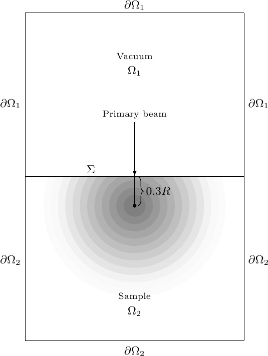
The SEM chamber consists of two main parts – the vacuum and the sample. Considering a cross-section, we assume a rectangular outer boundary Fig. 1, which can be further adjusted to take the actual geometry into account. The domain is further divided into two equal parts, where one represents the sample and the other the vacuum chamber. The Poisson equation (1) is considered on the whole domain ( and ), whereas, equations (2)-(5) are solved on the lower domain () only.
Depending on the material in contact with the sample two types of boundary conditions are common: Dirichlet conditions at ohmic contacts, and Robin conditions at Schottky and similar semi-insulating contactsmarkowichsemiconductor . The boundary of the sample domain consists of the Dirichlet part (where the sample is in contact with the walls of the SEM chamber or another highly conducting material), and the Robin part (sample-vacuum interface). At ohmic contacts (sides and the bottom of ) the space charge vanishes, i.e.,
| (9) |
Furthermore, the system is in thermal equilibrium there, which is expressed by the relation
| (10) |
From the above relations, we have
| (11) |
We also assume homogeneous Dirichlet conditions for the potential on the wall of the SEM chamber. i.e.
| (12) |
which could be easily adjusted to account for any finite value of the electric potential.
The dielectric-vacuum surface recombination model can been obtained as a simplification of the SRH modelzeghbroeck2012principles and leads to a somewhat unusual Robin-type boundary condition at the sample-vacuum interface. Namely, it is a semi-insulating contact for the electrons and an insulating contact for the holes (since holes cannot exist in vacuum):
| (13) | ||||
| (14) |
where is the surface recombination velocity (SRV) for electrons and denotes the unit outward normal vector on the boundary . This parameter has an important role in the model and will be discussed later. In fact, the insulating condition (14) can be also considered a semi-insulating contact with its surface recombination velocity set to zero ().
The intrinsic carrier density has been considered as the initial condition
| (15) |
III Beam model
III.1 Impact of an individual primary electron
When an electron beam illuminates the sample some of the primary electrons will reflect as backscattered electrons (for silicon oxide on average ), while the rest penetrates the sample and produces a large number of secondary electrons/holes.
It is important to realize that the DDR model (1)–(7) describes the equilibrium transport of charged particles with the distribution of kinetic energies either depending only on the (effective) temperature of the sample or simply being stable throughout the simulation time. However, the impact of the primary electron and its immediate aftermath are not equilibrium processes. Yet, since typical dielectric samples are made of dense materials, the numerous collisions will lead to the thermalization of all generated secondary particles shortly after the PE impact, so that their subsequent transport can indeed be modelled by (1)–(7). The precise rate of this thermalization is not known, but could be obtained with dedicated Monte-Carlo simulations maslovskaya2013physical , which are beyond the scope of the present paper. Here, we simply assume that all the secondary particles are in equilibrium by the time the primary electron looses most of its kinetic energy.
To account for the initial non-equilibrium transport we introduce an effective source model based on the available experimental data about the secondary charge distribution inside dielectrics. Moreover, since most of the SE emission happens during this initial non-equilibrium stage (in practice as well as in our simulations), the surface recombination velocity of the sample-vacuum interface (discussed below) allows further fine-tuning of the model using the material-dependent experimental SE yield data.
Mathematically, the injection of electrons is described by the terms and in the right hand sides of the continuity equations (2) and (4). In our model these source functions consist of two factors. The first factor represents the density of charge at the end of the ionization stage following the impact by a primary electron. The second purely temporal factor approximates the dynamics of the ionization stage, i.e., the build-up of the secondary charge during the first picosecond after collision. Thus, the source function has the form
| (16) |
where is the charge distribution function depending on the effective energy of the primary electron, as will be explained shortly, and is the following logistic function:
| (17) | ||||
where is the Malthusian parameter and is an initial condition related to the so-called carrying capacity ranging from 0 to 1. The values for and used in our calculations are reported in Table 1. We choose to be the logistic function since pair creation is an avalanche-type process and as such is mathematically similar to the population growth.
In (16) denotes the thermalization time, which is taken here to be approximately the time of the ballistic flight of the primary electron. Special relativity provides a simple relation between the velocity of a primary electron and its energy:
| (18) |
where is the speed of light in vacuum. The time of flight can be estimated by dividing the penetration depth (will be explained below) by this velocity (or a twice lower ‘average’ velocity). In either case it appears that for the relevant range of primary energies is in the order of seconds, i.e., extremely short with respect to the average time between electron impacts in a typical SEM beam. If this estimate is correct, then the DDR model is indeed applicable to the charge dynamics not only on large time scales, but also on the scale of individual impacts.
Let denote the maximum penetration depth by the primary electrons with initial energy . There exist several empirical formulas for . For example, the experimental results by Potts potts1987effect indicate that is given by:
| (19) |
where is the mass density of the sample material in and is in keV. On the other hand, theoretical considerations by Kanaya and Okayama kanaya1972penetration lead to
| (20) |
where is the atomic number, is the atomic mass and is in keV. The following composite formula proposed by Fitting fitting1974transmission has been used by several authors fitting1976multiple ; fitting2002cathodoluminescence ; meyza2003secondary ; touzin2006electron ; gaber1984energy :
| (21) |
where is in . Here we employ the most recent estimate by Fitting fitting2011secondary :
| (22) |
where is in and is in keV.
According to several studiesfitting1977electron ; cornet2008electron ; touzin2006electron the actual distribution of the secondary electrons and holes is well-approximated by a three-dimensional Gaussian function with its focus located below the vacuum-sample interface:
| (23) |
where is the mean creation energy for one SE, is the yield factor close to one, and
| (24) |
The constant is proportional to the fraction of backscattered PE. For silicon, silicon dioxide, and aluminium oxide, with , can be obtained from:
| (25) |
where is in eV and is in keV.
To account for the action of the surface potential on the primary electron, we introduce the effective energy , where is the time of impact, which should be applied in the distribution function instead of , thus arriving at:
| (26) | ||||
where is given by (22) and the pair creation energy depends on the material of the sample viatouzin2006electron
| (27) |
with denoting the energy gap of the material in eV.
The total numbers of secondary electrons and holes corresponding to the distribution (26) can now be estimated as
| (28) | ||||
showing that approximately of the effective energy is spent on the creation of charge pairs, which generally agrees with MC simulations. According to (28) the number of secondary electrons generated by one primary electron is somewhere between hundreds and thousands. Hence, we may expect the drift-diffusion-reaction approach to be a reasonable approximation at this scale.
Thus we take the for holes in (16) to be equal to as introduced in (26). Whereas for the electrons we recall that the primary electron is still present in the sample at . Hence, we adjust the coefficient in front of the exponent in the function so that it features one additional particle upon the integration (28). Thus, the factors of eq. (16) are
| (29) | ||||
where depends on the surface electric potential at the time of impact. Of course, the source functions proposed here are only approximations. Nevertheless, they are based on the best experimental evidence and first principles calculations available to date.
III.2 Bombardment and temporal smoothing
Depending on the beam current primary electrons may arrive at an average rate as high as tens of millions per second. Previous applications of the drift-diffusion-reaction approach typically describe the SEM beam as a constant flux of electrons. The goal of the present paper is to avoid the latter approximation and directly consider, say, , primary electrons arriving at times , . Thus, one obtains a pulsed source where the next PE arrives in a medium with some residual charge left from the impact of the previous PE.
Although, we gain some valuable insights about the subsurface charge dynamics and the effect of beam current, it is obviously too time consuming to consider bombardments of a sample by a large number of electrons in this way. Hence, a different approach is needed to study saturation effects at larger time scales. Also, the SE yield calculations on the level of single PE’s, although possible, are hard to justify and interpret.
The main technical challenge preventing direct large-scale simulations with our method is the pulsed nature of the source terms requiring many time steps to be performed by the solver between electron impacts. A way to reduce the computational burden is to derive a smoother function describing the behavior of source terms at larger time scales. In the limit such a smoother source function should approach the constant beam currents of the other DDR models.
To achieve this we employ a temporal average of our source function, which also mimics the way the SEM response is measured (time-averaged yield, rather than the yield due to individual PE’s). The average value of over a period of time between the impacts can be expressed as
| (30) |
and is a time-independent function. In what follows we call this a time-uniform or simply a uniform source.
Unfortunately, smoothing of the source has its price. Due to the presence of nonlinear terms in (1)–(7), solutions obtained with a time-averaged source term will not be the exact time-averaged values of the unknowns, but only the approximations thereof. Hence, to apply the DDR approach at both time scales successfully one needs to define constitutive relations and material parameters, such as the surface recombination velocity, for each scale separately. This is the so-called homogenization problem, typical for spatial multiscale analysis in physics (e.g. effective medium problem in electrodynamics).
Further, although a uniform source switched on at may be expected to eventually produce a steady-state distribution of charge, it is an open theoretical question whether the actual pulsed source leads to the corresponding periodic charge variations.
IV Numerical method
IV.1 Numerical scaling
To avoid numerical difficulties and maintain the accuracy of the solution, a simple scaling of variables has been performed. To this end we introduce a set of characteristic dimensionless quantities. We denote the characteristic length scale by , the characteristic time scale by and the characteristic density scale by . The numerical values of these dimensionless parameters relevant to the scale of the present problem are
| (31) |
There is a relation between these values ( and ) that doesn’t change the form of the equations, so that one only needs to introduce the rescaled versions for some of the constitutive parameters:
| (32) | ||||
Also the boundary and initial conditions should be rescaled, since, e.g. the rescaled version of the surface recombination velocity is given by:
| (33) |
IV.2 FEM solver
We employ the finite element method (FEM) for the numerical solution of the coupled system (1)–(7) and implement it as a solver within the COMSOL Multiphysics package. Although, there are many predefined modules and solvers in COMSOL, none of them can be directly applied with the present problem. The closest match is the semiconductor module. However, it is neither suited for studying the two different domains defined above, i.e., for equation (1) and for the rest, nor does it allow to incorporate the additional equations (3) and (5). Therefore, we have opted for building a new model using the general PDE and the ODE/DAE interfaces of COMSOL.
Since the charge densities may be extremely concentrated around the impact zone and form very thin layers near the vacuum-sample interface, a careful discretization strategy is required. To achieve sufficient accuracy one is advised to use the adaptive mesh with refinement in the impact zone and at the interface as well as the second-order Lagrange shape functions. A fully coupled approach with Newton-Raphson solver and adaptive time-stepping algorithm has shown the best performance with the present problem.
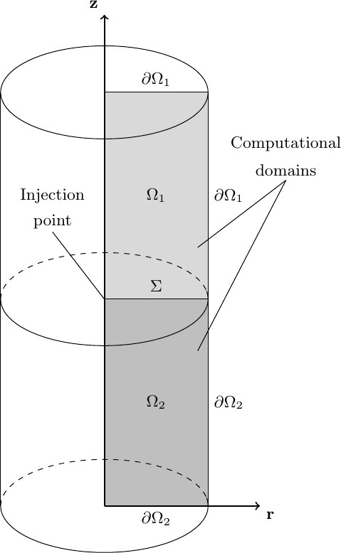
The computational complexity of the problem prohibits a full three-dimensional (3D) simulation of realistic domains with sufficient spatial resolution on a standard PC. Nevertheless, one can obtain 3D results for certain configurations at a typical two-dimensional (2D) cost by exploiting their symmetry. Consider, for example, the cylindrical geometry presented in Figure 2. In the cylindrical coordinate system the PE beam impinging along the -axis corresponds to the source term and boundary conditions independent of the angular coordinate . The solution will also be independent of and the original 3D model is reduced to a 2D model in the -coordinates. To arrive at the corresponding FEM solver the PDE’s (1), (2) and (4) must be written in the so-called weak form, which is derived in the Appendix.
V Numerical experiments
V.1 Parameters and parameter-tuning
It is clear that the values of the many constitutive parameters in the equations (1)–(7) may have considerable influence on the results of simulations. In the ideal situation these parameters are either measured in dedicated experiments or computed from the first principles of quantum physics. While this status-quo has long been established with the usual semiconductor materials, the data for insulators are virtually absent. Often, very different values for the same parameter are reported in the literature, which could be the result of varying sample properties, experimental conditions, or even trivial human errors (see e.g. detrapping rates in hwang2009drift and vasudevan1991numerical ). In particular, there is a lot of uncertainty about the parameters of recombination processes in the bulk and at interfaces. With this in mind we have made a selection of typical values for two distinct dielectrics shown in Table 1.
| Parameter | Unit | ||
|---|---|---|---|
| (ref.kwo2001properties ) | (ref.meyza2003secondary ) | ||
| (ref.renoud2004secondary ) | (ref.hughes1979generation ) | ||
| (ref.renoud2004secondary ) | |||
| (ref.vasudevan1991numerical ) | cm2 | ||
| (ref.vasudevan1991numerical ) | cm2 | ||
| (ref.renoud2004secondary ) | cm s-1 | ||
| (ref.hughes1979generation ) | s | ||
| (ref.helms1994silicon ) | (ref.meyza2003secondary ) | g cm-3 | |
| (ref.meyza2003secondary ) | eV | ||
| (ref.renoud2004secondary ) | cm-3 | ||
| (ref.hwang2009drift ) | s-1 | ||
| 25 | 25 | s-1 | |
*This value could not be found in literature and has been chosen by analogy with the relation between the electron and hole mobilities in .
In the boundary condition (13) the surface recombination velocity plays an important role analogous to the reflection coefficient of the current-based approach. In the literature the SRV is mostly discussed and measured for the metal-oxide-semiconductor interfaces. With respect to our case, which is a vacuum-semiconductor interface, the only reference that could be found refers to Germanium under ion bombardmentPhysRev.112.793 , reporting the value of . Considering the SRV to be material-dependent we believe that its value should be determined based on the consistency between the results of the present model and dedicated experiments.
The SE yield is defined as the number of secondary electrons emitted through the sample-vacuum interface and picked up by the detector per one incident electron. The importance of the SE yield stems from the fact that it is one of the few directly measurable quantities in SEMDatabase . Monte Carlo simulations of the SE yield are also available renoud2004secondary ; renoud2002monte ; kieft2008refinement ; ding2001monte . Therefore, in the tuning of the SRV parameter one would mostly be relying on the SE yield data as a function of the PE energy. In the present continuous approximation the SE yield is computed as the flux density through the boundary integrated over this boundary and over time from to , and divided by the number of PE’s that arrived at the sample during that time interval.
The following steps describe a simple optimization procedure for tuning the value of SRV:
-
•
Let be the SE yield measured fro PE’s with energy .
-
•
Let be the initial guess for the SRV, and let be the SE yield computed by the DDR solver with the SRV set to .
-
•
For sufficiently close to the true (optimal) value we can assume a linear relation:
(34) Since, obviously, , the coefficient can be obtained as , so that .
-
•
Compute with the DDR solver.
-
•
If is sufficiently close to , then stop and set . Otherwise, continue with as the new initial guess.
In principle, this process should be repeated with the SE yield data for a whole range of PE energies . Unless changes in significantly alter the temperature of the sample, the SRV of a given material is supposed to be independent of . Hence, if the corresponding tuned values of for some material are all close to each other, then we have an additional confirmation that the DDR method is working properly.
We conclude this section with a word of caution concerning the use of SE yield in determining the SRV. First of all, typical SE yield data correspond to some kind of stationary regime. It is known, however, that the SE yield keeps changing after the start of bombardment for quite a long time. Hence, we can compare the results of simulations with experimental data and tune the parameter only upon bombardment of the sample with a sufficiently large number of PE’s. In our approach such long-time simulations can only be performed with the time-uniform source. This means, however, that the tuned value of will be effective in nature.
Secondly, numerical experiments demonstrate that the electron flux through the sample-vacuum interface is not only time-dependent, but also depends on the extent of the sample and the proximity of ohmic contacts or other conducting materials to the beam’s entry point. Hence, one may expect different SE yield values with different samples of the same material.
V.2 Impact of a single primary electron
In this section we investigate the events following the injection of a single primary electron into a neutral dielectric sample. The goal of these numerical experiments is to estimate the space-time scales of the dynamics separately for all four particle species, i.e., , , , and , as well as the total charge density and the potential . In particular, these simulations will help us to demonstrate that despite the poor mobility and diffusivity of dielectrics, the drift and diffusion of free charges is generally much faster than the characteristic time scales of the charging process.
We focus on two common materials featured in many of the previous studies, namely, on the oxides and . As one can see from the data of Table 1 the difference between these materials is in the values of the relative permittivity ( has a smaller ), the electron and hole mobilities ( is relatively more conductive), and the mass density ( has a smaller density). The effective values of the SRV, cm/s for and cm/s for , were obtained with the optimization procedure explained above and typical experimental SE yield data barnardmeasurements ; yong1998determination ; Database using the time-uniform source model. Below we focus on a fixed PE energy keV.
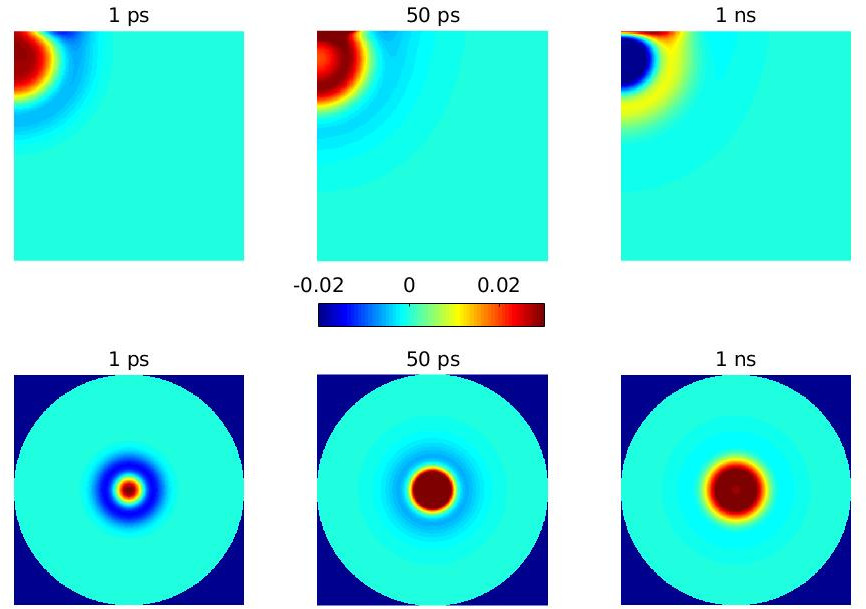
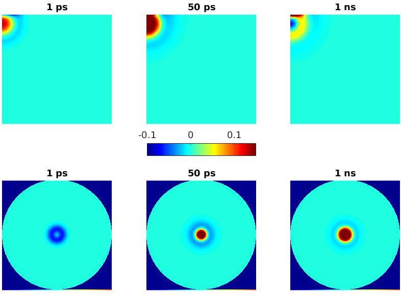
Figures 3 and 4 show the snapshots of the time evolution of the four charge species in the two materials. As can be seen from the upper-left images of these figures, the smaller mass density of means, see eq. (22), that with the same the maximum PE penetration depth and the center of the initial charge distribution are deeper for than for . The overall shapes of the initial charge distribution are different as well, see eq’s. (26) and (29), with the one of being broader. Hence the DDR dynamics starts with different initial states in these materials.
The generation of charge pairs by ionization takes place in the period of 1 picosecond after injection (=1 ps). Note that in our model the processes of recombination and trapping begin already at . At the density of free electrons is already beginning to decrease. In fact, the density of free electrons reaches its maximum of and for and , respectively, at around ps. The density of free holes reaches its maximum roughly at ps and remains constant till the end of the generation period . The maximum density of free holes in this stage for is and for is .
As expected, the density of trapped electrons and holes initially increases with time reaching, respectively, (at ) the values of and in , and and in . The lower density for the trapped holes compared with trapped electrons is due to the smaller trapping cross sections. In the density of trapped electrons reaches its maximum of at ps. Then, for more that ns, which is a relatively long time, no change is seen in the distribution of trapped electrons. After that the maximum density of trapped electrons starts to decrease dropping to at s. For the trapped holes, reaching the maximum density takes much longer time compared to the trapped electrons. The density of trapped holes keeps increasing at s and reaches its maximum of at ns. The maximum density for trapped holes at time ns is and at s the density of the trapped holes is . A similar dynamics of trapped particles is observed in .
During the first microsecond a fast decrease in the density of free electrons and a slower decrease in the density of free holes is observed owing to the relatively strong trapping of electrons and a weaker trapping of holes. In the major drop in the density of free electrons happens during the first ps. The maximum density of free electrons is at ps and reaches almost the intrinsic carrier density of the material at s. At ps the density of free holes is higher than that of the free electrons ().
The interplay of the four charge species leads to the total charge density resembling an expanding spherical wave with initially a positive charge region in the middle surrounded by a shell of negative charge followed by a negative middle region with a positive shell. Due to the emission of electrons the initial predominantly negative charge at the sample-vacuum interface is gradually replaced by the positive charge. In , the positive charge reaches its maximum of C/cm3 at the surface at ps and the negative charge has the maximum of (in the sens of absolute value) C/cm3 at ns and is situated close to the surface . In , the positive charge increases its maximum of C/cm3 at the surface at time ps and the negative charge has the maximum of C/cm3 in the center of impact zone at time ns.
Obviously, the electric potential closely follows the distribution of the total charge. Initially we observe a positive potential in the middle of the impact zone surrounded by a shell of weak negative potential. For example, in at the beginning a positive potential with the maximum of V is observed stretching across the sample-vacuum interface. A shell of weak negative potential is situated around this positive central region and appears inside the sample only. After a few hundred picoseconds, a transition occurs which results in a different situation for potential and that is the negative potential appears in the middle with shells of positive and negative potentials, respectively. The minimal value achieved by the potential during the first microsecond is V in which is situated in the center of impact zone and in the period of to ns.
V.3 Electron bombardment
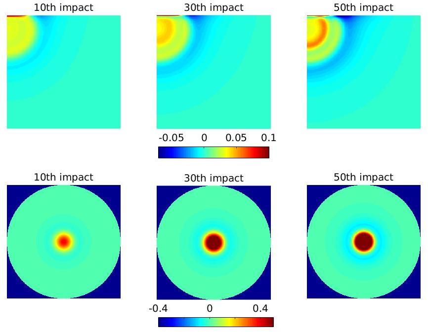
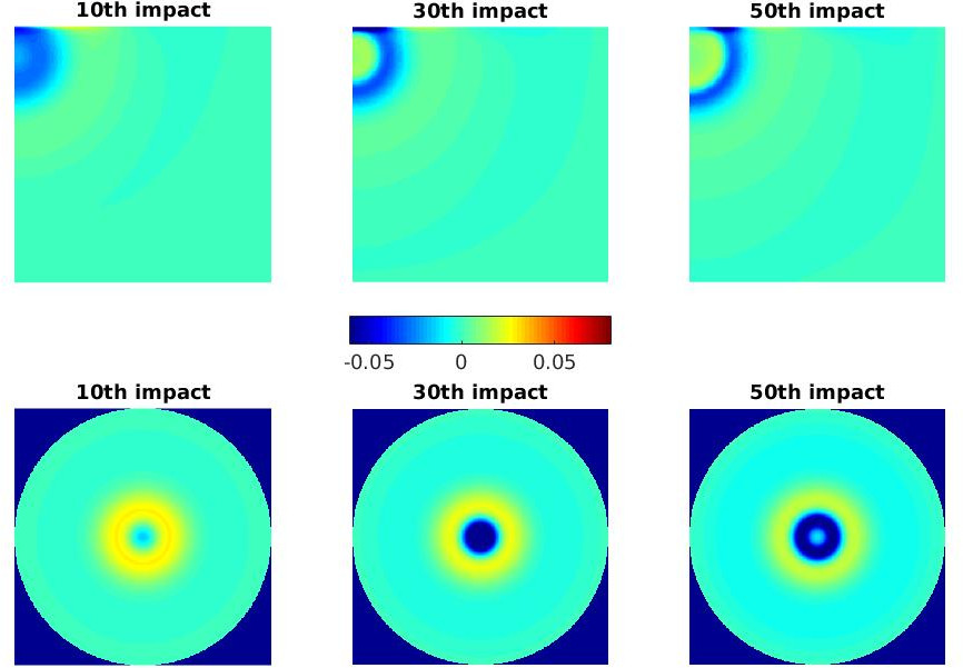
The electron gun of a typical SEM is able to produce PE currents in the range of pico to nano Ampéres (i.e. average interval between PE impacts from nano to picoseconds). The charge dynamics following the impact of a single PE, analyzed in the previous section, clearly shows that the next electron faces highly variable conditions in the sample depending on the time of its arrival.
Since the main features of the charge dynamics in and are essentially similar, we restrict our discussion to the latter material. In this section a sample is considered under focused beams with the currents of 160 nA and 160 pA (average times between PE impacts are ps and ns, respectively). To illustrate the nontrivial effect of the varying PE current the results in Figures 5 and 6 are presented for the same number of PE impacts in both beams that, obviously, correspond to different illumination times.
We start with the higher current of 160 nA modelled as a sequence of PE’s arriving with exact one picosecond intervals between them. Figure 5 shows the evolution of the total charge density during the first 50 impacts. On the fine temporal scale (not shown) we observe that the densities of free electrons and holes reach their maxima of and , respectively, at the end of the generation (ionization) stage after impacts and decrease afterwards.
The maximum density of trapped electrons reaches its maximum (the density of trapping sites ) for the first time at ps (after 30 PE impacts) inside the impact zone. A similar local saturation for the trapped holes does not happen during the first 50 PE’s, although, their density grows.
Similar to the aftermath of a single PE impact we observe a (semi) spherical wave of charge density emerging from the impact zone. However, now it remains a growing positive charge zone surrounded by the shell of negative charge without the charge-sign oscillation as in Figure 3. At the very beginning the positive charge has access to the surface, but towards the th impact a layer of negative charge prevents the positive charge from touching the surface. The maximum positive charge of C/cm3 is observed at the end and at the surface (lower-left image of Figure 5). The positive charge in the center of the expanding zone increases to C/cm3 towards the end (upper-right image of Figure 5). The negative charge remains confined to a shell around the positive charge. This shell becomes distorted by growing thicker with time along the sample-vacuum interface with the distance from the injection point, thus, reaching the maximum value of C/cm3 at the th impact. In the beginning and at time ns, the postive potential reaches its maximum of V in the center of impact zone and the negative potential reaches the minimum of V at the end of this initial bombardment period.
Next, we consider the beam current of 160 pA corresponding to one nanosecond intervals between PE impacts. Again, for a very short time after each impact, an increase in the density of free electrons is observed, which, after less that ns, drops to the almost the intrinsic carrier density of the material. The maximum of occurs at the end of the generation (ionization) stage. The density of free holes reaches its maximum of in the middle of the generation stage.
For about ps after each impact an increase in the density of the trapped electrons is seen after which the density remains constant until the next impact. Comparing this with the previously considered higher current we observe that now it takes a longer time ( ns) but less impacts ( PE impacts) for the density of the trapped electrons to reach the density of trapping sites in the middle of the impact zone. Similarly to the previous higher current, the density of trapped holes does not reach the trapping site density during the considered bombardment period.
Comparing the surface charge of the high (Figure 5, bottom) and low (Figure 6, bottom) currents we see that with the higher current, the positive charge at the injection point is present surrounded by a ring of negative charge, whereas with the lower current the charge at the injection point is negative surrounded by a ring of positive charge (Figure 5 bottom). In fact, with the pA current the positive surface charge is also seen, but not at the time of impact. Subsequently, after each impact, the positive potential is observed at the center of impact zone and after a few hundred picoseconds it is replaces with a negative potential. In the middle of the ionization time, both positive and negative potentials reach thier maxima of 0.17 V and -0.07 V, respectively.
Apart from the absence of rapid charge oscillation in the expanding spherical wave pattern, one can notice another substantial difference with the dynamics of Figure 3. Namely, the visible speed of expansion of the charged zone is much slower under the bombardment conditions, than during a single impact. Later we shall see that this speed of expansion roughly corresponds to the growth of the zone occupied by the trapped charges.
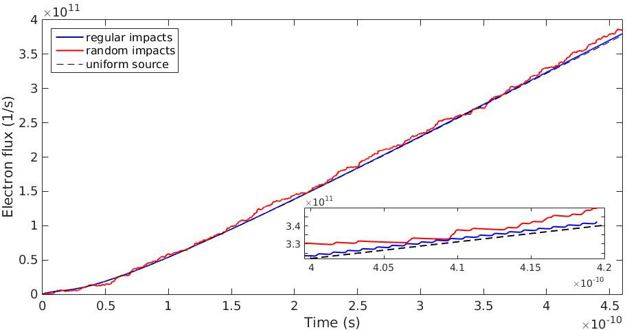
We have extended the simulation to PE impacts (at nA) and compared the idealistic source with periodic impacts considered above with the more realistic source whose PE’s impact the sample at time instants drawn from the Poisson distribution. Another purpose of this -impact simulation is to test the applicability of the time-uniform source model, see eq. (30). Figure 7 shows the electron flux through the sample-vacuum interface obtained by the pulsed model with regular and random impacts as well as time-uniform source model. The result shows that for this relatively short period at the beginning of the bombardment all three fluxes are in good agreement with each other. Based on these promising results, simulations for longer intervals of time can be carried out with the time-uniform source model.
V.4 Steady state
From the mathematical point view no steady-state solution exists with the pulsed source model (where each PE impact is modelled individually). At most, one can expect a time-periodic solution if PE impacts happen at regular intervals. The time-uniform source may, on the other hand, result in a solution that converges to a steady state for . In this section we investigate the large behaviour of the time-uniform source model in various circumstances.
Figures 8–11 show the simulation results by the time-uniform source model in the case of the high beam current of 160 nA. The electron flux through the sample-vacuum interface in Fig. 8 shows that a steady state starts around 400 nanoseconds in this case. To confirm that this, indeed, is a steady state we initiate the pulsed-source bombardment of the sample with the initial conditions set to the time-uniform steady-state solution. If such a steady state is stable, then the corresponding charge distributions and potential could be in the neighbourhood of a time-periodic solution expected in the case of the pulsed-source model with impacts at regular intervals. As can be seen from the magnified portion of the flux plot in Fig. 8, the flux computed with the pulsed-source model, indeed, appears to oscillate around the time-uniform flux.
The evolution of the surface charge shown in Fig. 8 starts with the positive charge at the injection point surrounded by a ring of negative charge. However, as the images show, after a few nanoseconds, this negative charge ring is removed by an outward-going (surface) wave and the positive charge settles in the center as a steady state. This positive charge grows up to the value of C/.
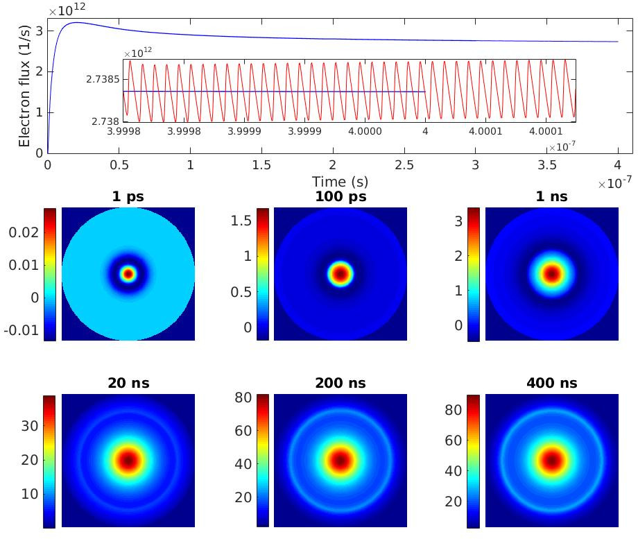
This behaviour and other features of the total charge dynamics are strongly influenced by the evolution of the trapped charge density shown in Fig. 9. As one can see, the trapped charges rapidly reach their saturation value in the impact zone, after which this saturated trapped-charge zone spreads outwards towards the ohmic boundaries. The electron trapping process and the spread of the corresponding zone is slightly faster than that of the holes (due to the higher mobility and trapping cross-section of the electrons). This, in particular, explains the presence of a slowly spreading negative shell in the top images of Figures 5–6. Also, around ns, a surface channel reaching the omic contacts developes, consisting of saturated trapped holes. It provides a path free of trapping for the positive charge transport along the sample vacuum interface. The latter can explain the saturation of the positive surface charge density shown in Fig. 8.
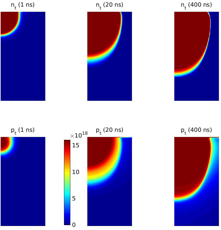
Further, the steady state with this beam current is characterized by the densities of free electrons and holes around and , respectively. The evolution of potential is shown in Fig. 10. It can be noted that potential follows the surface charge behavior, starting as a negative ring around a positive impact region. Then, the negative potential moves to the ohmic boundaries with time, and, after a few nanoseconds, the positive potential dominates in the sample as well as the vacuum close to the interface. A weak negative potential is observed below the positive one, however, it disappears after a few nanosecond.
Since in the present simulations, and both the trapped electrons and the trapped holes reach their saturation values almost everywhere (thus, effectively neutralizing the total trapped charge), the positive potential at large is the result of free rather than trapped holes. For example at ns, the free charge, , at the center of the surface is about while the trapped charge, , at the surface and around the injection point is almost homogeneous and around zero and close to the ohmic contact is .
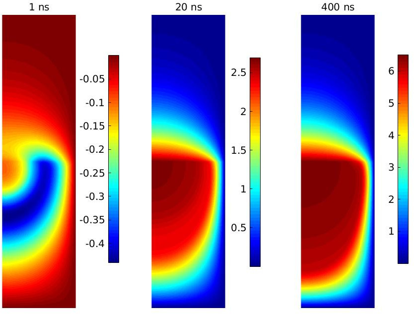
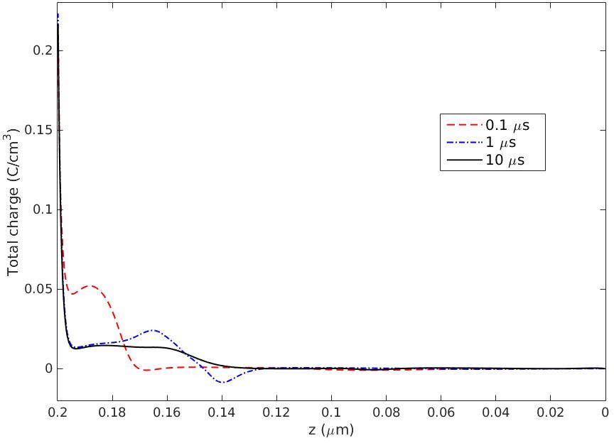
The evolution of the total charge along the beam direction when the beam current is nA is shown in Fig. 11, where the charge is displayed at three different time instants. The slight spatial advance of the saturated trapped-electron zone with respect to the saturated trapped-holes zone may explain the slowly expanding negative charge shell. As mentioned above, in the equilibrium state the sample is positively charged by the free holes. At this stage the trapped electrons and holes cancel each other, whereas, the free electrons disappear not only at the ohmic contacts, but through the sample-vacuum interface as well.
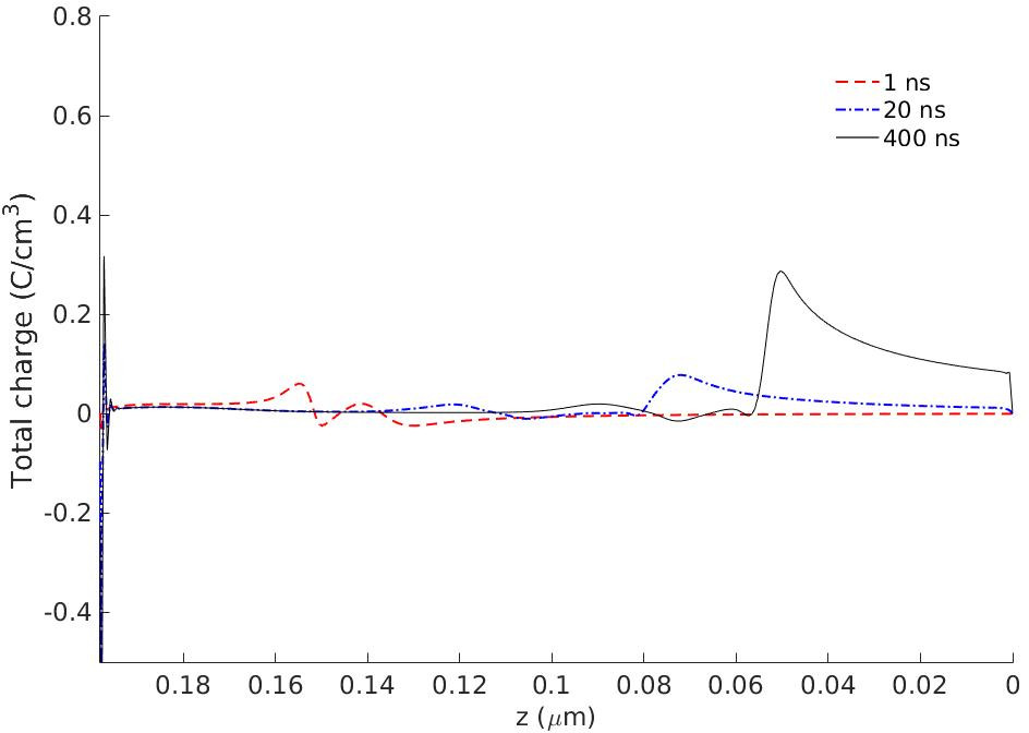
Figure 12 shows the simulation results with the lower pA beam current. The electron flux through the sample-vacuum interface demonstrates that the system reaches the steady state at a later time, compared to the previous higher nA current, but with fewer PE impacts. A significant difference is observed between the free charge distributions for these two values of beam currents. In particular, the shapes of the free electrons and free holes distributions in the steady state are same in the case of higher nA beam current. Whereas, the difference between these distributions at pA is obvious from the images of Fig. 12. The maximum density of free electrons is at the center of the impact zone, while for the free holes it is at the surface. The overall positive potential in the steady state is the result of the excess of free holes at the surface.
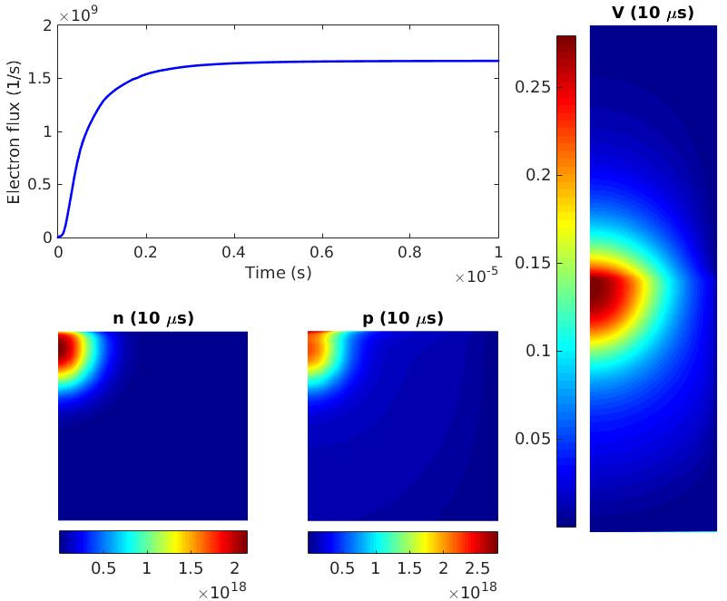
The total charge distribution along the beam direction for the beam current of pA is shown in Fig. 13. It is apparent that the spatial variations in the total charge density happen closer to the sample-vacuum interface (at depths less than nm) if compared to the higher nA beam current. Also, the surface charge remains positive from the start of the process.
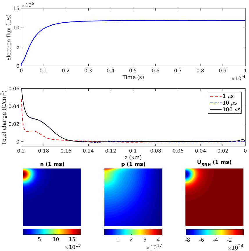
Finally, we consider an even lower pA beam current. The electron flux through the sample-vacuum interface in Fig. 14 and comparison with the previously obtained fluxes due to higher beam currents bring us to the conclusion that the flux rate and the time it takes to reach the steady state are roughly proportional to the beam current. Yet the number of PE impacts to reach the steady state is roughly inversely proportional to the beam current. The total charge distribution along the beam direction shown in Fig. 14 demonstrates that, compared to the pA current, the significant spatial variations happen closer to the sample-vacuum interface, approximately within the depth of nm. The system reaches the steady state around ms. The densities of free electrons and holes reach the maxima of and , respectively.
This simulation confirms that a lower beam current results in significant differences in the densities and spatial distribution between the free electrons and the free holes. At lower beam current the free electrons tend to concentrate at the center of the impact zone at some distance to the sample-vacuum interface, while the free holes are densely concentrated at the interface (see Fig. 14).
The lower-right image of Fig. 14 shows the spatial distribution of the recombination term , with the highest rate of achieved in the steady state. In the beginning of the process the recombination occurs at the center of the impact zone and at the sample-vacuum interface, approximately at the same rate. After a short time (few microseconds), the recombination is mostly active around the center of the impact zone due to the low density of free electrons at the surface. The highest recombination rates of and in the steady state are obtained with the beam currents of 160 pA and 160 nA, respectively. These results indicate that the recombination rate increases almost linearly with the beam current. Also, the variation of the recombination rate with the beam current clearly shows that applying a constant recombination rate in computational models does not reflect the actual recombination process in dielectric samples under SEM.
The SE yield can be calculated from the electron flux through the sample-vacuum interface shown in Figures 8, 12, and 14. A clear discrepancy in the measured SE yield of insulators is found in the literature, which can be attributed to the differences in the assumptions and conditions of the experiments. The present simulations, where the only varying parameter is the applied beam current, show that the SE yield increases with the beam current (provided all other conditions are fixed). The SE yields obtained here for the particular sample under focused beam currents of pA, pA, and nA are: , , and , respectively, which are, generally, within the range of experimental values reported in the literature. In fact, we observe a weak (logarithmic) dependence of the SE yield on the beam current. The experimental values of the SE yield for the (steam formed) sample in the database by Joy Database are: , , and . The measured SE yield for the (quartz) sample in barnardmeasurements is approximately . Whereas, according to the experiment of Yong et al. yong1998determination , the SE yield of a “wet and sputtered” silicon dioxide is found to be greater than .
Conclusions
We have proposed a fully self-consistent drift-diffusion-reaction model augmented with a dynamic charge trapping model for the quantitative numerical investigation of the electron beam interaction with dielectric samples. The pulsed and non-equilibrium nature of the charge injection mechanism and the back reaction of the accumulated charge on the incoming primary electrons are incorporated in the model through an explicit semi-empirical source formula. We have presented and compared two approaches to the charge injection problem. The first one is a pulsed source model reflecting the actual discrete nature of the electron beam. The second approach reduces the computational burden by applying a temporal average of the actual pulsed source function, which allows simulation at much longer time scales. Our results confirm the agreement between these two approaches in the initial stage and in the saturation regime.
The proposed model features a Robin-type semi-permeable boundary condition at the sample-vacuum interface reflecting the fact that the electrons are allowed to go through the boundary, while holes are not. We have devised a simple optimization procedure to deduce the surface recombination velocity (SRV) of dielectrics in vacuum from the experimental SE yield data.
The results of our simulations clearly demonstrate the need for the dynamic trapping equations in computational models of this kind. The trapping dynamics, namely, the time evolution of the spatial distributions of the trapped charge densities, has a major influence on (and helps to explain) the total charge distribution within the sample and the apparent transients in the surface charge density (in the high-current regime).
Inclusion of the dynamic generation-recombination model is also deemed necessary, since, as it turns out, the recombination rate depends on the beam current. Other quantities depend either strongly or weakly on the beam current as well, e.g., the local charge densities in the steady state show a linear dependence, whereas, the dependence of the SE yield turns out to be logarithmic.
Another conclusion of our study that requires a deeper mathematical analysis is the apparent existence of a time-periodic steady state in the considered system of equations for a pulsed source with PE impacts at regular intervals observed in the neighborhood of the steady-state solution for an averaged time-uniform source.
Acknowledgements
The authors acknowledge the partial financial support of the FEI Company (Netherlands) and many fruitful discussions with Dr. S. Sluyterman and Dr. E. Bosch (both with FEI). Thanks are also due to Professor B.J. Thijsse (Delft University of Technology), who gave us valuable counsel in the early stages of this work. Finally, we thank the anonymous reviewers for many thoughtful comments and suggestions.
Appendix A Weak form
Consider the partial differential equations (1), (2), and (4) in the axisymmetric geometry (see Fig: 2):
| (35) | ||||
| (36) | ||||
| (37) | ||||
To derive the weak formulation we integrate over the cross-sectional area () arriving at the following form of the equation (35):
| (38) |
where is the weight function. Integrating the highest-order terms by parts we obtain:
| (39) | ||||
| (40) | ||||
where is the outward unit normal vector to the boundary. Therefore, the weak form of the equation (35) can be written as:
| (41) | ||||
or
| (42) |
where and .
References
- (1) J Barnard, I Bojko, and N Hilleret. Measurements of the secondary electron emission of some insulators. Internal Note (CERN), 1997.
- (2) Kurt Binder and Dieter Heermann. Monte Carlo simulation in statistical physics: an introduction. Springer Science & Business Media, 2010.
- (3) J-P Colinge and Cynthia A Colinge. Physics of semiconductor devices. Springer Science & Business Media, 2005.
- (4) Nadège Cornet, Dominique Gœuriot, Christelle Guerret-Piecourt, Denyse Juvé, Daniel Tréheux, Matthieu Touzin, and H-J Fitting. Electron beam charging of insulators with surface layer and leakage currents. Journal of Applied Physics, 103(6):064110, 2008.
- (5) ZJ Ding, XD Tang, and R Shimizu. Monte carlo study of secondary electron emission. Journal of Applied Physics, 89(1):718–726, 2001.
- (6) H-J Fitting. Transmission, energy distribution, and se excitation of fast electrons in thin solid films. Physica status solidi (a), 26(2):525–535, 1974.
- (7) H-J Fitting, T Barfels, AN Trukhin, B Schmidt, A Gulans, and A Von Czarnowski. Cathodoluminescence of ge+, si+, and o+ implanted sio 2 layers and the role of mobile oxygen in defect transformations. Journal of non-crystalline solids, 303(2):218–231, 2002.
- (8) H-J Fitting, H Glaefeke, and W Wild. Electron penetration and energy transfer in solid targets. physica status solidi (a), 43(1):185–190, 1977.
- (9) H-J Fitting, H Glaefeke, W Wild, and G Neumann. Multiple scattering of fast electrons and their secondary electron generation within semi-infinite targets. Journal of Physics D: Applied Physics, 9(17):2499, 1976.
- (10) H-J Fitting and M Touzin. Time-dependent start-up and decay of secondary electron emission in dielectrics. Journal of Applied Physics, 108(3):033711, 2010.
- (11) H-J Fitting and M Touzin. Secondary electron emission and self-consistent charge transport in semi-insulating samples. Journal of Applied Physics, 110(4):044111, 2011.
- (12) M Gaber and H-J Fitting. Energy-depth relation of electrons in bulk targets by monte-carlo calculations. physica status solidi (a), 85(1):195–198, 1984.
- (13) Zhang Hai-Bo, Li Wei-Qin, and Cao Meng. Leakage current simulation of insulating thin film irradiated by a nonpenetrating electron beam. Chinese Physics Letters, 29(4):047901, 2012.
- (14) C Robert Helms and Edward H Poindexter. The silicon-silicon dioxide system: Its microstructure and imperfections. Reports on Progress in Physics, 57(8):791, 1994.
- (15) RC Hughes. Generation, transport, and trapping of excess charge carriers in czochralski-grown sapphire. Physical Review B, 19(10):5318, 1979.
- (16) Inchan Hwang, Christopher R McNeill, and Neil C Greenham. Drift-diffusion modeling of photocurrent transients in bulk heterojunction solar cells. Journal of Applied Physics, 106(9):094506, 2009.
- (17) DC Joy. A database of electron-solid interactions, revision 08-1, 2008.
- (18) K_ Kanaya and S Okayama. Penetration and energy-loss theory of electrons in solid targets. Journal of Physics D: Applied Physics, 5(1):43, 1972.
- (19) E.R. Kieft. Monte carlo simulation for sem imaging of charging samples: a status overview. Technical report, Philips Research Europe, 2007.
- (20) Erik Kieft and Eric Bosch. Refinement of monte carlo simulations of electron–specimen interaction in low-voltage sem. Journal of Physics D: Applied Physics, 41(21):215310, 2008.
- (21) J Kwo, M Hong, AR Kortan, KL Queeney, YJ Chabal, RL Opila, DA Muller, SNG Chu, BJ Sapjeta, TS Lay, et al. Properties of high k gate dielectrics gd2o3 and y2o3 for si. Journal of Applied Physics, 89(7):3920–3927, 2001.
- (22) Wei-Qin Li, Kun Mu, and Rong-Hou Xia. Self-consistent charging in dielectric films under defocused electron beam irradiation. Micron, 42(5):443–448, 2011.
- (23) Wei-Qin Li and Hai-Bo Zhang. The positive charging effect of dielectric films irradiated by a focused electron beam. Applied Surface Science, 256(11):3482–3492, 2010.
- (24) Wei-Qin Li and Hai-Bo Zhang. The surface potential of insulating thin films negatively charged by a low-energy focused electron beam. Micron, 41(5):416–422, 2010.
- (25) H. H. Madden and H. E. Farnsworth. High-vacuum studies of surface recombination velocity for germanium. Phys. Rev., 112:793–800, Nov 1958.
- (26) PA Markowich, C Ringhofer, and C Schmeiser. Semiconductor equations. Springer-Verlag New York, Inc., 1990.
- (27) AG Maslovskaya. Physical and mathematical modeling of the electron-beam-induced charging of ferroelectrics during the process of domain-structure switching. Journal of Surface Investigation. X-ray, Synchrotron and Neutron Techniques, 7(4):680–684, 2013.
- (28) X Meyza, D Goeuriot, C Guerret-Piécourt, D Tréheux, and H-J Fitting. Secondary electron emission and self-consistent charge transport and storage in bulk insulators: Application to alumina. Journal of applied physics, 94(8):5384–5392, 2003.
- (29) JE Potts, H Cheng, S Mohapatra, and TL Smith. Effect of elastic strain on the energy band gap in heteroepitaxially grown znse. Journal of applied physics, 61(1):333–336, 1987.
- (30) R Renoud, F Mady, C Attard, J Bigarre, and J-P Ganachaud. Secondary electron emission of an insulating target induced by a well-focused electron beam–monte carlo simulation study. physica status solidi (a), 201(9):2119–2133, 2004.
- (31) R Renoud, F Mady, and JP Ganachaud. Monte carlo simulation of the charge distribution induced by a high-energy electron beam in an insulating target. Journal of Physics: Condensed Matter, 14(2):231, 2002.
- (32) Raphaël Renoud, C Attard, JP Ganachaud, Sophie Bartholome, and Alain Dubus. Influence on the secondary electron yield of the space charge induced in an insulating target by an electron beam. Journal of Physics: Condensed Matter, 10(26):5821, 1998.
- (33) Alexander L Shluger, Keith P Mckenna, Petr V Sushko, D Muñoz Ramo, and AV Kimmel. Modelling of electron and hole trapping in oxides. Modelling and Simulation in Materials Science and Engineering, 17(8):084004, 2009.
- (34) Matthieu Touzin, Dominique Goeuriot, Christelle Guerret-Piécourt, Denyse Juvé, Daniel Tréheux, and H-J Fitting. Electron beam charging of insulators: A self-consistent flight-drift model. Journal of applied physics, 99(11):114110, 2006.
- (35) B Van Zeghbroeck. Principles of electronic devices. University of Colorado, 2011.
- (36) V Vasudevan and J Vasi. A numerical simulation of hole and electron trapping due to radiation in silicon dioxide. Journal of applied physics, 70(8):4490–4495, 1991.
- (37) YC Yong, JTL Thong, and JCH Phang. Determination of secondary electron yield from insulators due to a low-kv electron beam. Journal of applied physics, 84(8):4543–4548, 1998.
- (38) Hai-Bo Zhang, Wei-Qin Li, and Meng Cao. Space charge characteristics of an insulating thin film negatively charged by a low-energy electron beam. Journal of electron microscopy, page dfr099, 2012.
- (39) Hai-Bo Zhang, Wei-Qin Li, and Dan-Wei Wu. Contrast mechanism due to interface trapped charges for a buried sio2 microstructure in scanning electron microscopy. Journal of electron microscopy, 58(1):15–19, 2009.