Further author information: (Send correspondence to J.M.C.)
J.M.C.: E-mail: chowmj@us.ibm.com, Telephone: 1 914 945 2695
Characterizing a Four-Qubit Planar Lattice for Arbitrary Error Detection
Abstract
Quantum error correction will be a necessary component towards realizing scalable quantum computers with physical qubits. Theoretically, it is possible to perform arbitrarily long computations if the error rate is below a threshold value. The two-dimensional surface code permits relatively high fault-tolerant thresholds at the 1% level, and only requires a latticed network of qubits with nearest-neighbor interactions. Superconducting qubits have continued to steadily improve in coherence, gate, and readout fidelities, to become a leading candidate for implementation into larger quantum networks. Here we describe characterization experiments and calibration of a system of four superconducting qubits arranged in a planar lattice, amenable to the surface code. Insights into the particular qubit design and comparison between simulated parameters and experimentally determined parameters are given. Single- and two-qubit gate tune-up procedures are described and results for simultaneously benchmarking pairs of two-qubit gates are given. All controls are eventually used for an arbitrary error detection protocol described in separate work [Corcoles et al., Nature Communications, 6, 2015].
keywords:
Superconducting qubits, quantum computing, quantum error correction1 INTRODUCTION
To deal with the inherently fragile nature of physical qubit systems, quantum error correction [1] protocols are required to make fault-tolerant quantum computing a reality. Superconducting qubits have begun to enter a phase of study where the challenge is to continue to build larger inter-connected networks for realization of quantum error correction protocols. The surface code [2, 3, 4] is one particularly attractive fault-tolerant quantum error correction architecture, requiring only nearest-neighbor interactions, and physically realized through a simple square lattice arrangement. Furthermore, threshold error levels for the surface code are low at 1%, which are reasonable targets for superconducting qubit systems which have continued to show steady progress in coherence times [5, 6, 7].
Pairing the ideas of the surface code error correction protocol with superconducting qubits has already resulted in multiple important demonstrations. Ancilla-based bit-flip parity detection in networks of three superconducting qubits have been shown and characterized [8, 9]. Dealing with classical bit-flip parity errors was taken a step further through the implementation of a 5 and 9-qubit repetition code [10] in a linear network of superconducting transmon qubits, successfully showing increased preservation of an encoded bit-flip state with larger code distance. A true quantum code was implemented in a 4-qubit two-by-two lattice arrangement of transmons, with the ability to detect an arbitrary single-qubit quantum error to a codeword of two code qubits, via measurement of two ancilla qubits, one for bit-flip errors, and one for phase-flip errors [11]. In this Proceeding, we expand on that particular work by going into further detail on device design and simultaneous gate characterization in the 4-qubit lattice experiment from Ref. 11.
2 Device Design and Parameters
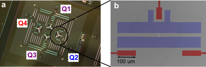
We construct a four-qubit lattice using four superconducting transmon qubits [12], connected in a ring arrangement with four coplanar waveguide quantum bus resonators [13], and each transmon qubit has an independent readout resonator. Every quantum bus connects two qubits, and every qubit is connected to two buses. The four-qubit device is shown in Fig. 1a with labels for each of the four qubits. The red (Q4) and blue (Q2) qubits are used for syndrome error detection, whilst the two purple qubits (Q1 and Q3) are code qubits. The four-qubit device is a small modification to the three-qubit half-plaquette device of Ref. 9. The major differences are the addition of one transmon, an additional readout resonator for that transmon, and two additional bus resonators for completing the lattice connectivity. We next describe the design of this transmon, along with reasoning for targeting particular circuit parameters and qubit properties. That is followed by a section describing experimentally obtained device parameters for the four-qubit device that we have studied, and we include a discussion about the comparison with the targeted simulation values.
2.1 Transmon design and parameter selection
An optical micrograph of the superconducting transmon qubit design used in both Refs. 9 and 11 is shown in Fig. 1b. The particular parameter regime which we aim for is strongly influenced by the need for high quality controls and readout of the qubits.
One key aspect of constructing our devices is to preserve the ability to perform high-fidelity two-qubit gates. Although there are a host of different implementations of two-qubit gates for superconducting qubits, the one which we focus on is the cross-resonance (CR) gate. The CR gate has the advantages that it can be performed with microwave control, and does not require dynamic tunability of the qubit frequencies. Details about the CR gate and interaction have been published previously [14, 15, 16], but functionally, there are two labeled qubits, a control qubit and a target qubit. A microwave drive onto the control qubit at the target transition frequency, will result in a control qubit state dependent rotation of the target qubit. Via proper calibration of this rotation, it is possible to realize either a controlled-NOT operation, or a rotation around the two-qubit axis (, where the notation follows with the control-qubit labeled first), which serves as the primitive for constructing gates from the two-qubit Clifford group [17].
Detailed experimental and theoretical study of the CR gate [18] with transmon qubits have shown that there is an optimal detuning window between the control and target transmon qubit frequencies which results in stronger interactions and hence faster gates. This detuning window corresponds to placing the target transmon transition frequency right between the two frequencies corresponding to the lowest two energy level differences of the control transmon. The devices we work with are fixed-frequency transmons (no SQUID loop for magnetic flux tunability), so as to avoid decoherence due to residual flux noise [19]. With fixed-frequency transmon devices, hitting this window comes down to having accurate control over the transmon capacitance values and the critical currents of the Josephson junctions. To that end, through multiple iterations of device designs and experimental extraction of transmon parameters, it has been observed that the primary cause of frequency fluctuations in nominally identical designs is critical current fluctuations on the order of , and to a lesser degree capacitance variation. As such, in order to design larger networks with many transmons that preserve the ability to perform reliable and fast CR gates between neighboring transmons, it is necessary to make this anharmonicity window large enough that even with the variation in transmon frequency from fabrication, that we will fall within the window. Future work will be aimed at minimizing these critical current fluctuations in order to avoid frequency collisions in even larger arrays of qubits.
For our four-qubit devices, we settle on a transmon capacitance that results in MHz of anharmonicity. With lowest energy level frequencies of GHz, this means with typical critical current fluctuations that we see on order of MHz of frequency spread, and that neighboring transmon devices will have a reasonable chance at hitting the CR gate window given their relative detuning. With this level of anharmonicity, it is also important to remain strictly around GHz, otherwise, any lower will result in the device not behaving in the transmon regime [12].
By narrowing down the transmon transition frequencies (5 GHz) and transmon anharmonicities (MHz), we are guided towards the selection of the readout resonator frequencies and quantum bus frequencies. In order to have high-fidelity readout, it is important to get in the regime where standard quantum-limited amplifiers can function. To pair specifically with Josephson parametric amplifiers [20] and superconducting low-inductance undulatory galvanometer amplifiers [21], we choose readout frequencies around 6.4-6.8 GHz, which fall within the tunable bandwidth for gain with such amplifiers. We then carefully select an appropriate coupling strength and readout resonator coupling capacitance so as to satisfy optimal readout fidelity conditions (as described in Ref. 22) and yet not be overly limited via Purcell-loss through the resonator [23]. Future work will entail integrating Purcell filters to permit faster readouts with stronger couplings, while avoiding spontaneous decay via the coupled resonator [24, 25, 26]. Similar considerations are taken into account for the bus resonators, with the added caveat that each transmon device must couple to two independent bus resonators. To avoid frequency collision between the readout resonators and the bus resonators, we choose 7.6 and 8.1 GHz for neighboring buses. The coupling strength to each transmon is chosen to be relatively large, MHz, so as to achieve strong CR interactions. With the transmons at 5 GHz, loss due to spontaneous emission into the bus cavities is also suppressed. Table 1 summarizes the targeted design values for various parameters for our devices. Capacitance simulations are done using ANSYS Q3D and we use network theory for a reduction to a minimal model.
| Quantity | Targeted | Q1 | Q2 | Q3 | Q4 |
| qubit transition frequency (GHz) | 5.3 | 5.303 | 5.101 | 5.291 | 5.415 |
| anharmonicity (MHz) | -339.9 | ||||
| critical current (nA) | 27 | 26.8 (27.2) | 25.1 (25.4) | 26.7 (27) | 27.8 (28.2) |
| qubit capacitance (fF) | 62 + | 65.5 (66.5) | 65.9 (66.9) | 65.3 (66.3) | 65.3 (66.3) |
| 45.7 | 45.0 | 42.4 | 44.7 | 46.5 | |
| charge dispersion (kHz) | 24.9 | 28.3 | 45.3 | 30.0 | 21.6 |
| from charge (ms) | 41 | 35.8 | 22.4 | 33.8 | 47.0 |
| readout resonator (GHz) | 6.5/6.7 | 6.494 | 6.695 | 6.491 | 6.693 |
| readout factor | 15000 | 10560 | 15200 | 22600 | 5530 |
| dispersive shift (MHz) | -1.6 | -1.5 | -1.0 | -1.25 | -1.4 |
| coupling to readout (MHz) | 94 | 89 | 94 | 82 | 92 |
| coupling capacitance (fF) | 5.5 | 5.4 | 5.7 | 5.0 | 5.3 |
| Purcell limited (s) | 69 | 70 | 182 | 182 | 40 |
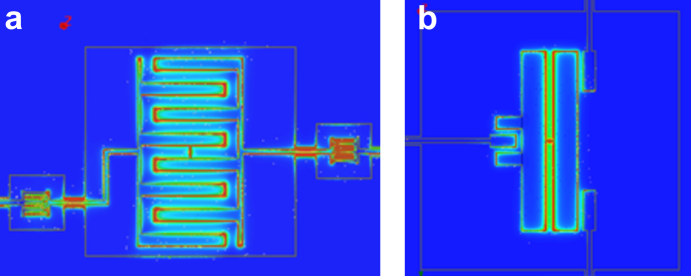
As seen in Fig. 1b, the transmon design has a very simplified parallel pad layout. This design departs from previous transmon schemes in which the capacitance is defined via interdigitated finger electrodes [17, 6]. The avoidance of finger capacitors for the transmon capacitance and for any coupling capacitance to bus or readout resonators is a conscious decision made to abate susceptibility and participation of lossy interfaces [27, 6, 28]. As an example, Fig. 2 shows two transmon designs which have been studied in our group. The first, Fig. 2a consists of a main transmon capacitor made of 30 m fingers with 30 m gaps. This device is similar to ones studied in single-qubit modalities as in Ref. 6. In those devices, it was observed phenomenologically that going to a larger finger and gap width for the interdigitated capacitance improved the quality factor of the underlying qubits, consistent with reducing the participation of substrate-air and substrate-metal interfaces in surface loss simulations. In addition, the old designs had a considerable part of the qubit capacitance in the couplers to the resonators. We subsequently moved to the current design as in Fig. 2b, which provides the capacitance via a parallel pad geometry and reduces the participation of the qubit capacitance in the couplers to the resonators.
The colored density plots in Fig. 2 are ANSYS HFSS simulated electric-field densities. Simulations of the electric-field participation in the substrate-air, metal-air, and substrate-metal interfaces are determined. To compare the two different geometries of Fig. 2, we find that the parallel pad configuration results in a reduction of the substrate-air interface participation by , metal-air interface participation by , and substrate-metal interface participation by . We attribute increased transmon quality factors to these changes to the design, but at this moment, we cannot yet pinpoint which of these are the most dominant factor for improvement.
2.2 Four-qubit device parameters and comparison to simulation
From our experiment with the four-qubit device, we find transition frequencies for Q1, Q2, Q3, and Q4 at 5.303, 5.101, 5.291, and 5.415 GHz, respectively along with corresponding measured anharmonicities all around MHz. From measurement of the interaction with the readout cavities, dispersive shift is found to be -1.5,-1.0,-1.25, and -1.4 MHz . Using these measured values, we complete the values of Table 1 with a comparison to the targeted values from simulation. We can see that for this device, in which the four qubits are fabricated with the same targeted design values, there is still a considerable spread in the qubit frequencies. Nonetheless, all qubits fall within the anharmonicity window which make it usable for nearest-neighbor two-qubit CR gates.
The readout resonators are designed at 6.5 and 6.7 GHz, and the experiment shows excellent agreement for these designs. There is some observed variation in the measured quality factors of the four resonators, which results in some differences in the expected Purcell decay channels for the four different qubits [23]. Future designs of these lattice devices will employ Purcell filtering [24] so as to allow for fast readout and still preserve qubit lifetimes. Nonetheless, good agreement between simulations and our actual experiments are important for further optimizing geometries to be incorporated into larger lattices of qubits for the surface code.
3 Calibrating Controls
Through standard sliding -pulse and spin echo sequences, we characterize the coherence times of the four-qubit device. We find energy relaxation times = , , , s and coherence times = , ,, s for Q1, Q2, Q3,and Q4 respectively. These experiments are performed repeatedly over the course of two days, to gather statistics and average values for the coherence times. Subsequently, we calibrate single-qubit gates for each of the four qubits as well as two-qubit CR gates between nearest neighbor qubits in the lattice.
All microwave pulses are applied using single-sideband (SSB) modulation of a carrier microwave tone using an arbitrary waveform generator. Using SSB ensures a well-defined phase relationship between the two quadratures for performing single-qubit rotations either around the -axis or -axis and avoids carrier leakage on resonance with the qubit transition. The single-qubit gates that are calibrated in our system include and rotations around the - and -axes of each qubit. First, the amplitudes are tuned up by measuring the cavity response after for up to 7. Then, we bootstrap off the tuned up pulse to find the appropriate amplitude via the pulse train , again for up to 7 pulses. Finally, the derivative-pulse shaping (DRAG) parameter [30] is tuned via the sequence . Further study into the accurate calibration of these single-qubit gates is the subject of separate work [31].
The two-qubit CR gates are calibrated in close analogy to single qubit amplitude calibrations. Following the refocusing sequence as described in Ref. 17, it is possible to define a two-qubit gate. An odd number of pulses are applied and the amplitude is adjusted so that for each the expected signal is halfway between 0 and 1 (in our experiment =5). Any amplitude miscalibrations lead to departures from this expected signal and are amplified for increasing .
In addition to amplitude we must also calibrate the phase of the pulse of the CR gate to the phase of the target qubit. The phase of the complete microwave pulse realizing the CR gate is tuned to match that of the microwave pulse which realizes the single qubit rotations on the target. This is done by applying the pulse sequence [9] . The denotes the rotation axis defined by the CR pulse and the goal is to calibrate to match an rotation on the target qubit. In the case of an -rotation we expect the signal to be halfway between 0 and 1 for each and miscalibrations of the phase lead to deviations that are amplified with increasing .
4 Simultaneous Gate Characterization and Validation
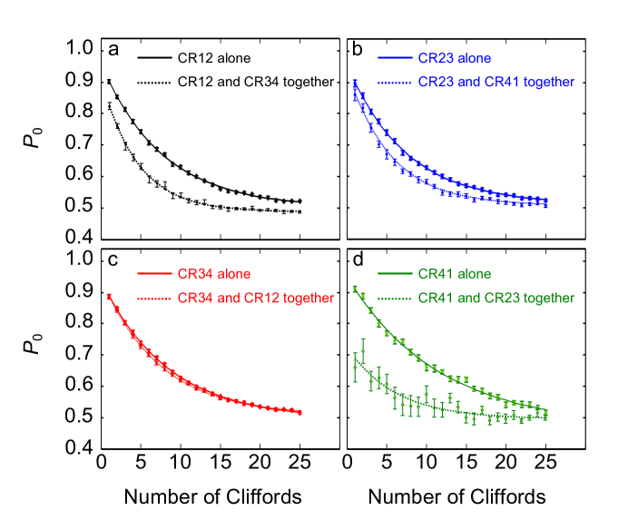
Having calibrated the single- and two-qubit gates for all qubits and all nearest neighbor CR operations, we apply the techniques of Clifford randomized benchmarking [32] (RB) to characterize the quality of the calibrated gates through an average gate fidelity. In this technique, random sequences of gates chosen from the Clifford group are constructed, paired with a final Clifford gate which returns the qubit to the ground state. Both single and two-qubit Clifford benchmarking are performed. Average sequence fidelity of this ground state versus an increasing number of Clifford gates is then plotted, and performed over many different randomized sequences of Cliffords. For single-qubit gates, we calibrate pulses of length 53.3 ns, and find average gate fidelities of , , , for Q1, Q2, Q3, and Q4 respectively. We also characterize the nearest-neighbor two-qubit CR gates via RB [17]. The averaged two-qubit RB sequence fidelity versus the number of Cliffords over 30 different randomizations is shown in Fig. 3 as the solid curves. From these curves, we extract gate fidelities of , , , for CR12, CR23, CR34, and CR41, respectively. Here the notation refers to a CR gate between Q and Q, with referencing the control qubit and referencing the target qubit.
Another important part of characterizing the gates for this four-qubit device is to look at crosstalk effects. To tackle this problem, we employ the technique of simultaneous RB [33]. By simultaneously applying randomized Clifford sequences to multiple qubits it is possible to get a bound on the amount of crosstalk errors in the system. A full table showing the effect of simultaneous RB, with all combinations of simultaneous application of RB experiments for the four qubits, is given in Ref. 11. Comparing the individual and simultaneous RB experiments,it is observed that the addressability error is 0.001 or lower in all cases for our single-qubit gates.
It is also possible to check simultaneous RB of the two-qubit gates. As the two-qubit gates involve two qubits at a time, it is only possible to run two sets of simultaneous gates: CR12 with CR34 at the same time, and CR23 with CR41 at the same time. The average sequence fidelity versus Clifford number in these simultaneous cases are also shown in Fig. 3 as the dashed lines. When CR12 and CR34 are simultaneously benchmarked, we now obtain fidelities of and for CR12 and CR34, respectively. CR12 has significantly worsened in this experiment, although CR34 is not very affected. Similarly, for CR23 and CR41, we now obtain fidelities of 0.9149 and 0.9241, respectively, which are both significantly lower than when the same gates are characterized independently.
It is clear that in three of the four two-qubit gate cases, the simultaneous application of the gates alter and degrade their performance. The exact nature of this crosstalk is the subject of further study and understanding it will help us control and construct larger lattices. Nonetheless, even with this level of addressability error, the quantum error detection experiments as described in Ref. 11 can still be run because many of the gates in that protocol are staggered and not run at the same time. Future work will address how to make these controls more robust to simultaneous operation, which may be necessary in more complicated algorithms.
5 Conclusions
In this Proceeding, we presented additional detail on the design rules for transmon qubits in the four-qubit lattice device used for arbitrary error detection in Ref. 11. We showed the comparison between designed parameters and experimentally extracted parameters. We also presented results of simultaneous application of control gates in the device. Looking ahead, the further exploration of addressability errors arising from two-qubit gates in a lattice of qubits will be critical to understanding how to control larger lattices of qubits for the surface code quantum error correction protocol.
Acknowledgements.
We thank M. B. Rothwell and G. A. Keefe for fabricating devices. We thank J. R. Rozen, J. Rohrs and K. Fung for experimental contributions. We acknowledge support from IARPA under contract W911NF-10-1-0324. All statements of fact, opinion or conclusions contained herein are those of the authors and should not be construed as representing the official views or policies of the U.S. Government.References
- [1] Shor, P. W., “Scheme for reducing decoherence in quantum computer memory,” Physical Review A 52(4), 2493–6 (1995).
- [2] Bravyi, S. and Kitaev, A., “Quantum codes on a lattice with boundary,” (1998). arXiv:quant-ph/9811052.
- [3] Raussendorf, R. and Harrington, J., “Fault-tolerant quantum computation with high threshold in two dimensions,” Physical Review Letters 98(19), 190504 (2007).
- [4] Fowler, A. G., Mariantoni, M., Martinis, J. M., and Cleland, A. N., “Surface codes: Towards practical large-scale quantum computation,” Physical Review A 86(3), 032324 (2012).
- [5] Paik, H., Schuster, D. I., Bishop, L. S., Kirchmair, G., Catelani, G., Sears, A. P., Johnson, B. R., Reagor, M. J., Frunzio, L., Glazman, L. I., Girvin, S. M., Devoret, M. H., and Schoelkopf, R. J., “Observation of High Coherence in Josephson Junction Qubits Measured in a Three-Dimensional Circuit QED Architecture,” Physical Review Letters 107(24), 240501 (2011).
- [6] Chang, J. B., Vissers, M. R., Corcoles, A. D., Sandberg, M., Gao, J., Abraham, D. W., Chow, J. M., Gambetta, J. M., Beth Rothwell, M., Keefe, G. A., Steffen, M., and Pappas, D. P., “Improved superconducting qubit coherence using titanium nitride,” Applied Physics Letters 103(1), 012602 (2013).
- [7] Devoret, M. H. and Schoelkopf, R. J., “Superconducting circuits for quantum information: An outlook,” Science 339(6124), 1169–1174 (2013).
- [8] Saira, O.-P., Groen, J. P., Cramer, J., Meretska, M., de Lange, G., and DiCarlo, L., “Entanglement Genesis by Ancilla-Based Parity Measurement in 2D Circuit QED,” Physical Review Letters 112(7) (2014).
- [9] Chow, J. M., Gambetta, J. M., Magesan, E., Abraham, D. W., Cross, A. W., Johnson, B. R., Masluk, N. A., Ryan, C. A., Smolin, J. A., Srinivasan, S. J., and Steffen, M., “Implementing a strand of a scalable fault-tolerant quantum computing fabric,” Nature Communications 5 (2014).
- [10] Kelly, J., Barends, R., Fowler, A. G., Megrant, A., Jeffrey, E., White, T. C., Sank, D., Mutus, J. Y., Campbell, B., Chen, Y., Chen, Z., Chiaro, B., Dunsworth, A., Hoi, I.-C., Neill, C., O’Malley, P. J. J., Quintana, C., Roushan, P., Vainsencher, A., Wenner, J., Cleland, A. N., and Martinis, J. M., “State preservation by repetitive error detection in a superconducting quantum circuit,” Nature 519(7541), 66–69 (2015).
- [11] Corcoles, A. D., Magesan, E., Srinivasan, S. J., Cross, A. W., Steffen, M., Gambetta, J. M., and Chow, J. M., “Demonstration of a quantum error detection code using a square lattice of four superconducting qubits,” Nature Communications 6 (2015).
- [12] Koch, J., Yu, T. M., Gambetta, J., Houck, A. A., Schuster, D. I., Majer, J., Blais, A., Devoret, M. H., Girvin, S. M., and Schoelkopf, R. J., “Charge-insensitive qubit design derived from the Cooper pair box,” Physical Review A 76, 042319 (2007).
- [13] Majer, J., Chow, J. M., Gambetta, J. M., Koch, J., Johnson, B. R., Schreier, J. A., Frunzio, L., Schuster, D. I., Houck, A. A., Wallraff, A., Blais, A., Devoret, M. H., Girvin, S. M., and Schoelkopf, R. J., “Coupling superconducting qubits via a cavity bus,” Nature 449, 443–447 (2007).
- [14] Paraoanu, G. S., “Microwave-induced coupling of superconducting qubits,” Physical Review B 74(14), 140504 (2006).
- [15] Rigetti, C. and Devoret, M., “Fully microwave-tunable universal gates in superconducting qubits with linear couplings and fixed transition frequencies,” Physical Review B 81(13), 134507 (2010).
- [16] Chow, J. M., Corcoles, A. D., Gambetta, J. M., Rigetti, C., Johnson, B. R., Smolin, J. A., Rozen, J. R., Keefe, G. A., Rothwell, M. B., Ketchen, M. B., and Steffen, M., “Simple All-Microwave Entangling Gate for Fixed-Frequency Superconducting Qubits,” Physical Review Letters 107(8), 080502 (2011).
- [17] Corcoles, A. D., Chow, J. M., Gambetta, J. M., Rigetti, C., Rozen, J. R., Keefe, G. A., Beth Rothwell, M., Ketchen, M. B., and Steffen, M., “Protecting superconducting qubits from radiation,” Applied Physics Letters 99(18), 181906 (2011).
- [18] Ware, M., Johnson, B. R., Gambetta, J. M., Ohki, T. A., Chow, J. M., and Plourde, B. L. T., “Cross-resonance interactions between superconducting qubits with variable detuning,” in preparation (2015).
- [19] Harlingen, D. J. V., Robertson, T. L., Plourde, B. L. T., Reichardt, P. A., Crane, T. A., and Clarke, J., “Decoherence in josephson-junction qubits due to critical-current fluctuations,” Physical Review B 70, 064517 (2004).
- [20] Johnson, J. E., Macklin, C., Slichter, D. H., Vijay, R., Weingarten, E. B., Clarke, J., and Siddiqi, I., “Heralded state preparation in a superconducting qubit,” Physical Review Letters 109(5), 050506 (2012).
- [21] Hover, D., Chen, Y.-F., Ribeill, G. J., Zhu, S., Sendelbach, S., and McDermott, R., “Superconducting low-inductance undulatory galvanometer microwave amplifier,” Applied Physics Letters 100(6) (2012).
- [22] Magesan, E., Gambetta, J. M., Corcoles, A. D., and Chow, J. M., “Machine learning for discriminating quantum measurement trajectories and improving readout,” (2014). arXiv:1411.4994 [quant-ph].
- [23] Houck, A. A., Schreier, J. A., Johnson, B. R., Chow, J. M., Koch, J., Gambetta, J. M., Schuster, D. I., Frunzio, L., Devoret, M. H., Girvin, S. M., and Schoelkopf, R. J., “Controlling the spontaneous emission of a superconducting transmon qubit,” Physical Review Letters 101(8), 080502 (2008).
- [24] Reed, M. D., DiCarlo, L., Johnson, B. R., Sun, L., Schuster, D. I., Frunzio, L., and Schoelkopf, R. J., “High-Fidelity Readout in Circuit Quantum Electrodynamics Using the Jaynes-Cummings Nonlinearity,” Physical Review Letters 105(17), 173601–173601 (2010).
- [25] Jeffrey, E., Sank, D., Mutus, J., White, T., Kelly, J., Barends, R., Chen, Y., Chen, Z., Chiaro, B., Dunsworth, A., Megrant, A., O’Malley, P., Neill, C., Roushan, P., Vainsencher, A., Wenner, J., Cleland, A., and Martinis, J. M., “Fast accurate state measurement with superconducting qubits,” Physical Review Letters 112(19) (2014).
- [26] Bronn, N. T., Magesan, E., Masluk, N. A., Chow, J. M., Gambetta, J. M., and Steffen, M., “Reducing spontaneous emission in circuit quantum electrodynamics by a combined readout/filter technique,” (2015). arXiv:1504.04353 [quant-ph].
- [27] Wenner, J., Barends, R., Bialczak, R. C., Chen, Y., Kelly, J., Lucero, E., Mariantoni, M., Megrant, A., O’Malley, P. J. J., Sank, D., Vainsencher, A., Wang, H., White, T. C., Yin, Y., Zhao, J., Cleland, A. N., and Martinis, J. M., “Surface loss simulations of superconducting coplanar waveguide resonators,” Applied Physics Letters 99(11), 113513 (2011).
- [28] Barends, R., Kelly, J., Megrant, A., Sank, D., Jeffrey, E., Chen, Y., Yin, Y., Chiaro, B., Mutus, J., Neill, C., O’Malley, P., Roushan, P., Wenner, J., White, T. C., Cleland, A. N., and Martinis, J. M., “Coherent josephson qubit suitable for scalable quantum integrated circuits,” Physical Review Letters 111(8) (2013).
- [29] Chow, J. M., Gambetta, J. M., Corcoles, A. D., Merkel, S. T., Smolin, J. A., Rigetti, C., Poletto, S., Keefe, G. A., Rothwell, M. B., Rozen, J. R., Ketchen, M. B., and Steffen, M., “Universal quantum gate set approaching fault-tolerant thresholds with superconducting qubits,” Physical Review Letters 109(6), – (2012).
- [30] Motzoi, F., Gambetta, J. M., Rebentrost, P., and Wilhelm, F. K., “Simple pulses for elimination of leakage in weakly nonlinear qubits,” Physical Review Letters 103(11), 110501–4 (2009).
- [31] Sheldon, S., Bishop, L. S., Magesan, E., Filipp, S., Chow, J. M., and Gambetta, J. M., “Characterizing errors on qubit operations via iterative randomized benchmarking,” (2015). arXiv:1504.06597 [quant-ph].
- [32] Magesan, E., Gambetta, J. M., and Emerson, J., “Scalable and robust randomized benchmarking of quantum processes,” Phys. Rev. Lett. 106(18), 180504 (2011).
- [33] Gambetta, J. M., Corcoles, A. D., Merkel, S. T., Johnson, B. R., Smolin, J. A., Chow, J. M., Ryan, C. A., Rigetti, C., Poletto, S., Ohki, T. A., Ketchen, M. B., and Steffen, M., “Characterization of addressability by simultaneous randomized benchmarking,” Physical Review Letters 109(24), 240504 (2012).